


Texas Instruments TLV2354IPW, TLV2354IN, TLV2354IDR, TLV2354ID, TLV2354MJB Datasheet
...TLV2354, TLV2354Y
LinCMOS QUADRUPLE LOW-VOLTAGE DIFFERENTIAL COMPARATORS
|
SLCS012B ± MAY 1992 ± REVISED MARCH 1999 |
|
|
D Wide Range of Supply Voltages |
D Fast Response Time . . . 200 ns Typ for |
2 V to 8 V |
TTL-Level Input Step |
D Fully Characterized at 3 V and 5 V |
D Extremely Low Input Bias Current |
D Very-Low Supply-Current Drain |
5 pA Typ |
240 µA Typ at 3 V |
D Output Compatible With TTL, MOS, and |
D Common-Mode Input Voltage Range |
CMOS |
|
|
Includes Ground |
D Built-In ESD Protection |
DHigh Input Impedance . . . 1012 Ω Typ
description |
symbol (each comparator) |
The TLV2354 consists of four independent, low-power comparators specifically designed for single power-supply applications and operateS with power-supply rails as low as 2 V. When powered from a 3-V supply, the typical supply current is only 240 µA.
IN +
OUT
IN ±
The TLV2354 is designed using the Texas Instruments LinCMOS technology and, therefore, features an extremely high input impedance (typically greater than 1012 Ω), which allows direct interfacing with high-impedance sources. The outputs are N-channel open-drain configurations that require an external pullup resistor to provide a positive output voltage swing, and they can be connected to achieve positive-logic wired-AND relationships. The TLV2354I is fully characterized for operation from ± 40°C to 85°C. The TLV2354M is fully characterized for operation from ± 55°C to 125°C.
The TLV2354 has internal electrostatic-discharge (ESD)-protection circuits and has been classified with a 1000-V ESD rating using Human Body Model testing. However, care should be exercised in handling this device as exposure to ESD may result in degradation of the device parametric performance.
AVAILABLE OPTIONS
|
|
|
|
PACKAGED DEVICES |
|
|
CHIP |
||
|
VIOmax |
|
|
|
|
|
|
||
TA |
SMALL |
CHIP |
CERAMIC |
PLASTIC |
|
CERAMIC |
|||
TSSOP |
FORM |
||||||||
at 25°C |
OUTLINE |
CARRIER |
DIP |
DIP |
FLATPACK |
||||
|
(PW)³ |
(Y) |
|||||||
|
|
(D)² |
(FK) |
(J) |
(N) |
(W) |
|||
|
|
|
|
||||||
± 40°C to |
5 mV |
TLV2354ID |
Ð |
Ð |
TLV2354IN |
TLV2354IPWLE |
Ð |
|
|
85°C |
|
||||||||
|
|
|
|
|
|
|
TLV2354Y |
||
|
|
|
|
|
|
|
|
||
± 55°C to |
5 mV |
Ð |
TLV2354MFK |
TLV2354MJ |
Ð |
Ð |
TLV2354MW |
||
|
|||||||||
125°C |
|
||||||||
|
|
|
|
|
|
|
|
||
|
|
|
|
|
|
|
|
|
|
² The D package is available taped and reeled. Add the suffix R to the device type (e.g., TLV2352IDR). ³ The PW packages are only available left-ended taped and reeled (e.g., TLV2354IPWLE).
These devices have limited built-in protection. The leads should be shorted together or the device placed in conductive foam during storage or handling to prevent electrostatic damage to the MOS gates.
Please be aware that an important notice concerning availability, standard warranty, and use in critical applications of Texas Instruments semiconductor products and disclaimers thereto appears at the end of this data sheet.
LINCMOS is a trademark of Texas Instruments Incorporated.
PRODUCTION DATA information is current as of publication date. Products conform to specifications per the terms of Texas Instruments standard warranty. Production processing does not necessarily include testing of all parameters.
Copyright 1999, Texas Instruments Incorporated
On products compliant to MIL-PRF-38535, all parameters are tested unless otherwise noted. On all other products, production processing does not necessarily include testing of all parameters.
POST OFFICE BOX 655303 •DALLAS, TEXAS 75265 |
1 |
TLV2354, TLV2354Y
LinCMOS QUADRUPLE LOW-VOLTAGE DIFFERENTIAL COMPARATORS
SLCS012B ± MAY 1992 ± REVISED MARCH 1999
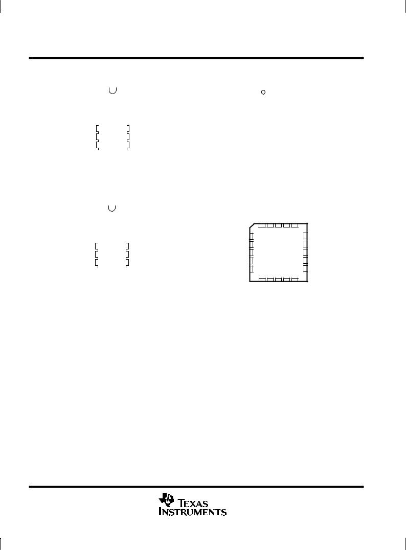
TLV2354I |
TLV2354I |
D OR N PACKAGE |
PW PACKAGE |
(TOP VIEW) |
(TOP VIEW) |
1OUT |
|
1 |
14 |
|
3OUT |
1OUT |
|
1 |
14 |
|
3OUT |
|
|
|
|
||||||||
2OUT |
|
2 |
13 |
|
4OUT |
2OUT |
|
2 |
13 |
|
4OUT |
|
|
|
|
||||||||
VDD+ |
|
3 |
12 |
|
VDD±/GND |
VDD+ |
|
3 |
12 |
|
VDD±/GND |
|
|
|
|
||||||||
2IN± |
|
4 |
11 |
|
4IN+ |
2IN± |
|
4 |
11 |
|
4IN+ |
|
|
|
|
||||||||
2IN+ |
5 |
10 |
|
4IN± |
2IN+ |
|
5 |
10 |
|
4IN± |
|
|
|
|
|||||||||
1IN± |
6 |
9 |
|
3IN+ |
1IN± |
|
6 |
9 |
|
3IN+ |
|
|
|
|
|||||||||
1IN+ |
7 |
8 |
|
3IN± |
1IN+ |
|
7 |
8 |
|
3IN± |
|
|
|
|
|||||||||
|
|
|
|
|
|
|
|
|
|
|
|
|
|
|
|
|
|
|
|
|
|
|
|
TLV2354M |
TLV2354AM, TLV2354M |
J OR W PACKAGE |
FK PACKAGE |
(TOP VIEW) |
(TOP VIEW) |
1OUT |
|
1 |
14 |
|
3OUT |
|
|
||||
2OUT |
|
2 |
13 |
|
4OUT |
|
|
||||
VDD+ |
|
3 |
12 |
|
VDD±/GND |
|
|
||||
2IN± |
|
4 |
11 |
|
4IN+ |
|
|
||||
2IN+ |
5 |
10 |
|
4IN± |
|
1IN± |
6 |
9 |
|
3IN+ |
|
1IN+ |
7 |
8 |
|
3IN± |
|
|
|
|
|
|
|
|
2OUT |
1OUT |
NC |
3OUT |
4OUT |
|
VDD+ |
3 |
2 |
1 |
20 19 |
VDD ±/GND |
|
4 |
|
|
|
18 |
||
NC |
5 |
|
|
|
17 |
NC |
2IN± |
6 |
|
|
|
16 |
4IN + |
NC |
7 |
|
|
|
15 |
NC |
2IN + |
8 |
|
|
|
14 |
4IN ± |
|
9 |
10 11 12 13 |
|
|||
|
1IN± |
1IN+ |
NC |
3IN± |
3IN + |
|
NC ± No internal connection
2 |
POST OFFICE BOX 655303 •DALLAS, TEXAS 75265 |
|
|
LinCMOS QUADRUPLE |
|
|
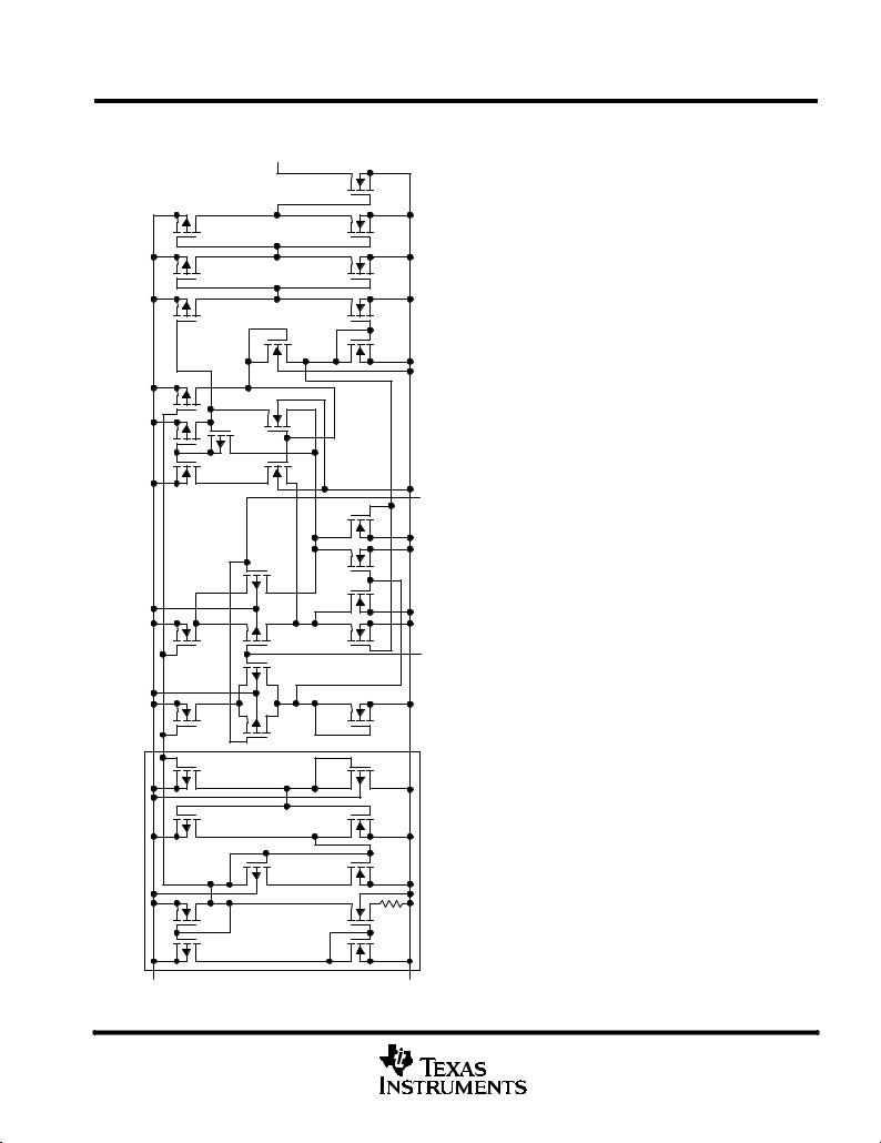
OUT |
|
|
IN ± |
|
|
IN + |
schematic |
Common to All Channels |
|
equivalent |
DD |
GND |
V |
TLV2254, TLV2254Y LOW-VOLTAGE DIFFERENTIAL COMPARATORS
SLCS012B ± MAY 1992 ± REVISED MARCH 1999
POST OFFICE BOX 655303• DALLAS, TEXAS 75265 |
3 |

TLV2354, TLV2354Y
LinCMOS QUADRUPLE LOW-VOLTAGE DIFFERENTIAL COMPARATORS
SLCS012B ± MAY 1992 ± REVISED MARCH 1999
TLV2354Y chip information
This chip, when properly assembled, displays characteristics similar to the TLV2354. Thermal compression or ultrasonic bonding may be used on the doped-aluminum bonding pads. This chip may be mounted with conductive epoxy or a gold-silicon preform.
BONDING PAD ASSIGNMENTS
|
|
|
|
(13) |
(12) |
(11) |
(10) |
(9) |
|
|
|
|
|
|
|
|
|||
|
|
(14) |
|
|
|
|
|
||
|
|
|
|
|
|
|
|
|
(8) |
|
|
|
|
|
|
|
|
||
65 |
|
|
|
|
|
|
|||
|
|
|
|
|
|
|
|
|
(7) |
|
|
(1) |
|
|
|
|
|
||
|
|
(2) |
(3) |
|
(4) |
(5) |
(6) |
||
|
|
|
|
|
|
|
|
|
|
|
|
|
|
|
|
|
|
|
|
|
|
|
|
|
90 |
|
|
|
|
|
|
|
|
|
|
|
|
|
|
|
|
|
|
VDD |
|
|
|
|
|
|
(7) |
|
|
(3) |
|
|
|
|
|
IN + |
+ |
|
|
|
|
|
|||
|
|
|
(1) |
|
OUT |
||||
|
|
|
|
||||||
|
|
|
|
|
|
|
|||
IN ± |
(6) |
± |
|
|
|
|
|||
|
|
|
|
||||||
|
|
|
|
|
|||||
|
|
|
(5) |
|
|
|
|||
|
|
|
|
|
|||||
|
|
|
+ |
|
|
IN + |
|||
OUT |
(2) |
|
|
|
|||||
|
|
|
|||||||
|
|
|
|
|
|
||||
|
|
± |
(4) |
|
|
IN ± |
|||
(9) |
|
|
|||||||
IN + |
|
|
|
||||||
|
|
|
|||||||
+ |
|
|
|
|
|
||||
|
|
|
(14) |
OUT |
|||||
|
|
|
|||||||
|
|
|
|
|
|
||||
IN ± |
(8) |
± |
|
|
|
|
|||
|
|
|
|
||||||
|
|
|
|
|
|||||
|
|
|
(11) |
IN + |
|||||
|
|
|
|||||||
|
|
|
+ |
||||||
OUT |
|
(13) |
|
|
|
||||
|
|
|
|
|
|
|
|||
|
|
± |
(10) |
IN ± |
|||||
|
|
|
|||||||
|
|
|
|
|
|
||||
(12) GND
CHIP THICKNESS: 15 MILS TYPICAL BONDING PADS: 4 × 4 MILS MINIMUM TJmax = 150°C
TOLERANCES ARE ± 10%.
ALL DIMENSIONS ARE IN MILS.
PIN (11) INTERNALLY CONNECTED TO BACKSIDE OF CHIP.
4 |
POST OFFICE BOX 655303 •DALLAS, TEXAS 75265 |
TLV2354, TLV2354Y
LinCMOS QUADRUPLE LOW-VOLTAGE DIFFERENTIAL COMPARATORS
SLCS012B ± MAY 1992 ± REVISED MARCH 1999
absolute maximum ratings over operating free-air temperature range (unless otherwise noted)²
Supply voltage, VDD (see Note 1) . . . . . . . . . . . . . . . . . . . . . . . . . . . . . . . . . . . . . . . |
. . . . . . . . . . . |
. . . . . . . . . . . 8 |
V |
Differential input voltage, VID (see Note 2) . . . . . . . . . . . . . . . . . . . . . . . . . . . . . . . |
. . . . . . . . . . . . |
. . . . . . . . . ± 8 |
V |
Input voltage range, VI . . . . . . . . . . . . . . . . . . . . . . . . . . . . . . . . . . . . . . . . . . . . . . . . . |
. . . . . . . . . . . . |
. . . ±0.3 to 8 |
V |
Output voltage, VO . . . . . . . . . . . . . . . . . . . . . . . . . . . . . . . . . . . . . . . . . . . . . . . . . . . . |
. . . . . . . . . . . . |
. . . . . . . . . . 8 |
V |
Input current, II . . . . . . . . . . . . . . . . . . . . . . . . . . . . . . . . . . . . . . . . . . . . . . . . . . . . . . . |
. . . . . . . . . . . . |
. . . . . . . ± 5 mA |
|
Output current, IO . . . . . . . . . . . . . . . . . . . . . . . . . . . . . . . . . . . . . . . . . . . . . . . . . . . . |
. . . . . . . . . . . . |
. . . . . . . 20 mA |
|
Duration of output short-circuit current to GND (see Note 3) . . . . . . . . . . . . . . . . |
. . . . . . . . . . . . |
. . . . . unlimited |
|
Continuous total power dissipation . . . . . . . . . . . . . . . . . . . . . . . . . . . . . . . . . . . . . |
See Dissipation Rating Table |
||
Operating free-air temperature range, TA: TLV2354I . . . . . . . . . . . . . . . . . . . . . . . |
. . . . . . . . . . . . |
±40°C to 85°C |
|
TLV2354M . . . . . . . . . . . . . . . . . . . . . . |
. . . . . . . . . . . |
±55°C to 125°C |
|
Storage temperature range . . . . . . . . . . . . . . . . . . . . . . . . . . . . . . . . . . . . . . . . . . . . . |
. . . . . . . . . . . |
±65°C to 150°C |
|
Lead temperature 1,6 mm (1/16 inch) from case for 10 seconds: D, N, or PW package . . . . . |
. . . . . . . 260°C |
||
Lead temperature 1,6 mm (1/16 inch) from case for 10 seconds: FK, J, or W package . . . . . |
. . . . . . . 300°C |
||
²Stresses beyond those listed under ªabsolute maximum ratingsº may cause permanent damage to the device. These are stress ratings only, and functional operation of the device at these or any other conditions beyond those indicated under ªrecommended operating conditionsº is not
implied. Exposure to absolute-maximum-rated conditions for extended periods may affect device reliability. NOTES: 1. All voltage values, except differential voltages, are with respect to network ground.
2.Differential voltages are at the noninverting input terminal with respect to the inverting input terminal.
3.Short circuits from outputs to VDD can cause excessive heating and eventual device destruction.
DISSIPATION RATING TABLE
PACKAGE |
TA ≤ 25°C |
DERATING |
TA = 85°C |
TA = 125°C |
|
POWER RATING |
FACTOR |
POWER RATING |
POWER RATING |
||
|
|||||
|
|
|
|
|
|
D |
950 mW |
7.6 mW/°C |
494 mW |
Ð |
|
FK |
1375 mW |
11.0 mW/°C |
715 mW |
275 mW |
|
J |
1375 mW |
11.0 mW/°C |
715 mW |
275 mW |
|
N |
1150 mW |
9.2 mW/°C |
598 mW |
Ð |
|
PW |
700 mW |
5.6 mW/°C |
364 mW |
Ð |
|
W |
700 mW |
5.5 mW/°C |
370 mW |
150 mW |
|
|
|
|
|
|
recommended operating conditions
|
|
MIN |
MAX |
UNIT |
|
|
|
|
|
|
|
Supply voltage, VDD |
|
2 |
8 |
V |
|
Common-mode input voltage, VIC |
VDD = 3 V |
0 |
1.75 |
V |
|
VDD = 5 V |
0 |
3.75 |
|||
|
|
||||
Operating free-air temperature, TA |
TLV2354I |
± 40 |
85 |
°C |
|
|
|
|
|||
TLV2354M |
± 55 |
125 |
|||
|
|
||||
|
|
|
|
|
POST OFFICE BOX 655303 •DALLAS, TEXAS 75265 |
5 |
TLV2354, TLV2354Y
LinCMOS QUADRUPLE LOW-VOLTAGE DIFFERENTIAL COMPARATORS
SLCS012B ± MAY 1992 ± REVISED MARCH 1999
electrical characteristics at specified free-air temperature²
|
|
|
|
|
|
|
TLV2354I |
|
|
|
|
|
PARAMETER |
TEST CONDITIONS |
T ³ |
|
|
|
|
|
|
UNIT |
|
|
|
VDD = 3 V |
|
|
VDD = 5 V |
|
|||||
|
|
|
|
A |
|
|
|
|
|
|
|
|
|
|
|
|
MIN |
TYP |
MAX |
MIN |
TYP |
MAX |
|
|
|
|
|
|
|
|
|
|
|
|
|
VIO |
Input offset voltage |
VIC = VICRmin, |
See Note 4 |
25°C |
|
1 |
5 |
|
1 |
5 |
mV |
Full range |
|
|
7 |
|
|
7 |
|||||
|
|
|
|
|
|
|
|
|
|||
|
|
|
|
|
|
|
|
|
|
|
|
IIO |
Input offset current |
|
|
25°C |
|
1 |
|
|
1 |
|
pA |
|
|
85°C |
|
|
1 |
|
|
1 |
nA |
||
|
|
|
|
|
|
|
|
||||
|
|
|
|
|
|
|
|
|
|
|
|
IIB |
Input bias current |
|
|
25°C |
|
5 |
|
|
5 |
|
pA |
|
|
85°C |
|
|
2 |
|
|
2 |
nA |
||
|
|
|
|
|
|
|
|
||||
|
|
|
|
|
|
|
|
|
|
|
|
|
Common-mode input |
|
|
25°C |
0 to 2 |
|
|
0 to 4 |
|
|
|
VICR |
|
|
|
|
|
|
|
|
|
V |
|
|
|
|
0 to |
|
|
0 to |
|
|
|||
voltage range |
|
|
Full range |
|
|
|
|
||||
|
|
|
1.75 |
|
|
3.75 |
|
|
|
||
|
|
|
|
|
|
|
|
|
|
||
|
|
|
|
|
|
|
|
|
|
|
|
IOH |
High-level output |
VID = 1 V |
|
25°C |
|
0.1 |
|
|
0.1 |
|
nA |
current |
|
Full range |
|
|
1 |
|
|
1 |
µA |
||
|
|
|
|
|
|
|
|||||
|
|
|
|
|
|
|
|
|
|
|
|
VOL |
Low-level output |
VID = ±1 V, |
IOL = 2 mA |
25°C |
|
115 |
300 |
|
150 |
400 |
mA |
voltage |
Full range |
|
|
600 |
|
|
700 |
||||
|
|
|
|
|
|
|
|
||||
|
|
|
|
|
|
|
|
|
|
|
|
IOL |
Low-level output |
VID = ± 1 V, |
VOL = 1.5 V |
25°C |
6 |
16 |
|
6 |
16 |
|
mA |
current |
|
|
|||||||||
|
|
|
|
|
|
|
|
|
|
|
|
|
|
|
|
|
|
|
|
|
|
|
|
IDD |
Supply current |
VID = 1 V, |
No load |
25°C |
|
240 |
500 |
|
290 |
600 |
µA |
|
|
|
|
|
|
|
|||||
Full range |
|
|
700 |
|
|
800 |
|||||
|
|
|
|
|
|
|
|
|
|||
|
|
|
|
|
|
|
|
|
|
|
|
² All characteristics are measured with zero common-mode input voltage unless otherwise noted. ³ Full range is ± 40°C to 85°C. IMPORTANT: See Parameter Measurement Information.
NOTE 4: The offset voltage limits given are the maximum values required to drive the output above 4 V with VDD = 5 V, 2 V with VDD = 3 V, or below 400 mV with a 10-kΩ resistor between the output and VDD. They can be verified by applying the limit value to the input and checking for the appropriate output state.
switching characteristics, VDD = 3 V, TA = 25°C
PARAMETER |
|
TEST CONDITIONS |
|
TLV2354I |
|
UNIT |
|
|
|
|
|
||||
|
MIN |
TYP |
MAX |
||||
|
|
|
|
|
|||
|
|
|
|
|
|
|
|
Response time |
RL = 5.1 kΩ, |
CL = 15 pF§, |
100-mV input step with 5-mV overdrive |
|
640 |
|
ns |
See Note 5 |
|
|
|
||||
|
|
|
|
|
|
|
|
|
|
|
|
|
|
|
|
§ CL includes probe and jig capacitance.
NOTE 5: The response time specified is the interval between the input step function and the instant when the output crosses VO = 1 V with VDD = 3 V or when the output crosses VO = 1.4 with VDD = 5 V.
switching characteristics, VDD = 5 V, TA = 25°C
PARAMETER |
|
TEST CONDITIONS |
|
TLV2354I |
UNIT |
|
|
|
|
||||
|
MIN |
TYP MAX |
||||
|
|
|
|
|
||
|
|
|
|
|
|
|
Response time |
RL = 5.1 kΩ, |
CL = 15 pF§, |
100-mV input step with 5-mV overdrive |
|
650 |
ns |
See Note 5 |
|
TTL-level input step |
|
200 |
||
|
|
|
|
|||
|
|
|
|
|
||
|
|
|
|
|
|
|
§ CL includes probe and jig capacitance.
NOTE 5: The response time specified is the interval between the input step function and the instant when the output crosses VO = 1 V with VDD = 3 V or when the output crosses VO = 1.4 with VDD = 5 V.
6 |
POST OFFICE BOX 655303 •DALLAS, TEXAS 75265 |
 Loading...