


Texas Instruments TLV2404IPWR, TLV2404IPW, TLV2404IN, TLV2404IDR, TLV2404ID Datasheet
...TLV2401, TLV2402, TLV2404 FAMILY OF 900-nA/Ch RAIL-TO-RAIL INPUT/OUTPUT OPERATIONAL AMPLIFIERS WITH REVERSE BATTERY PROTECTION
SLOS244 ± FEBRUARY 2000
DMicro-Power Operation . . . < 1 µA/Channel
DInput Common-Mode Range Exceeds the Rails . . . ±0.1 V to VCC + 5 V
DRail-to-Rail Input/Output
DGain Bandwidth Product . . . 5.5 kHz
DSupply Voltage Range . . . 2.5 V to 16 V
DSpecified Temperature Range
±TA = 0°C to 70°C . . . Commercial Grade
±TA = ±40°C to 125°C . . . Industrial Grade
DUltra-Small Packaging
±5-Pin SOT-23 (TLV2401)
±8-Pin MSOP (TLV2402)
DUniversal OpAmp EVM
description
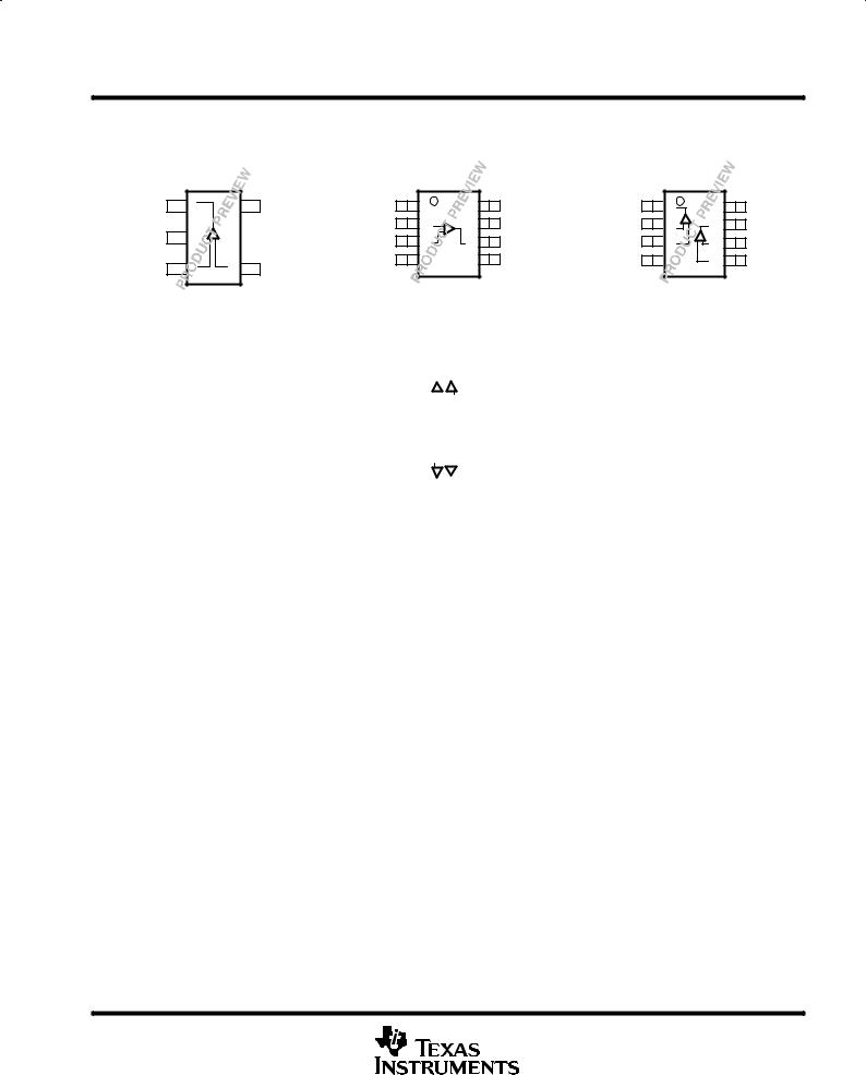
TLV2404
D, N, OR PW PACKAGE
(TOP VIEW)
1OUT |
|
|
1 |
|
|
|
|
|
|
|
|
14 |
|
|
4OUT |
|
|
|
|
|
|
|
|
|
|
|
|||||
1IN ± |
|
|
2 |
|
|
|
|
|
|
|
|
13 |
|
|
4IN ± |
1IN+ |
|
|
3 |
|
|
|
|
|
|
|
|
12 |
|
|
4IN+ |
|
|
|
|||||||||||||
VCC |
|
|
4 |
|
|
|
11 |
|
|
GND |
|||||
|
|
|
|
|
|
|
|||||||||
|
|
|
|
|
|
|
|||||||||
2IN+ |
|
|
5 |
|
|
|
|
|
|
|
|
10 |
|
|
3IN+ |
2IN ± |
|
|
6 |
|
|
|
|
|
|
|
|
9 |
|
|
3IN ± |
|
|
|
|
|
|
|
|
|
|
|
|
||||
2OUT |
|
7 |
|
|
|
|
|
8 |
|
|
3OUT |
||||
|
|
|
|
|
|
|
|
|
|
|
|
||||
|
|
|
|
|
|||||||||||
|
|
|
|
|
|
|
|
|
|
|
|
||||
|
|
|
|
|
|
|
|
|
|
|
|
|
|
|
|
SUPPLY CURRENT vs
SUPPLY VOLTAGE
The TLV240x family of single-supply operational amplifiers has the lowest supply current available today at only 900 nA per channel. Added to this is reverse battery protection making the device even more ideal for battery powered systems. And for harsh environments, the inputs can be taken 5 V above the positive supply rail without damage to the device.
The low supply current is coupled with extremely low input bias currents enabling them to be used with mega-Ω resistors making them ideal for portable, long active life, applications. DC accuracy is ensured with a low typical offset voltage as low as 390 µV, CMRR of 120 dB and minimum open loop gain of 130 V/mV at 2.7 V.
|
1.4 |
AV = 1 |
|
|
|
|
|
|
|
|
|
|
|
|
|
|
|
||
A/Ch |
1.2 |
VIN = VCC / 2 |
|
|
|
|
|
||
|
TA =25 °C |
|
|
|
|
|
|
||
|
1.0 |
|
|
|
|
|
|
|
|
± |
|
|
|
|
|
|
|
|
|
Current |
0.8 |
|
|
|
|
|
|
|
|
|
|
|
|
|
|
|
|
|
|
± Supply |
0.6 |
|
|
|
|
|
|
|
|
0.4 |
|
|
|
|
|
|
|
|
|
CC |
|
|
|
|
|
|
|
|
|
|
|
|
|
|
|
|
|
|
|
I |
0.2 |
|
|
|
|
|
|
|
|
|
|
|
|
|
|
|
|
|
|
|
0 |
|
|
|
|
|
|
|
|
|
0 |
2 |
4 |
6 |
8 |
10 |
12 |
14 |
16 |
|
|
|
VCC ± Supply Voltage ± V |
|
|
||||
The maximum recommended supply voltage is as high as 16 V and ensured operation down to 2.5 V, with electrical characteristics specified at 2.7 V, 5 V and 15 V. The 2.5-V operation makes it compatible with Li-Ion battery-powered systems and many micro-power microcontrollers available today including TI's MSP430.
All members are available in PDIP and SOIC with the singles in the small SOT-23 package, duals in the MSOP, and quads in TSSOP.
FAMILY PACKAGE TABLE
DEVICE |
NO. OF Ch |
|
PACKAGE TYPES |
|
UNIVERSAL |
|||
PDIP |
SOIC |
SOT-23 |
TSSOP |
MSOP |
EVM |
|||
|
|
|||||||
|
|
|
|
|
|
|
|
|
TLV2401² |
1 |
8 |
8 |
5 |
Ð |
Ð |
Refer to the EVM |
|
TLV2402² |
2 |
8 |
8 |
Ð |
Ð |
8 |
Selection Guide |
|
|
|
|
|
|
|
|
(Lit# SLOU060) |
|
TLV2404 |
4 |
14 |
14 |
Ð |
14 |
Ð |
||
|
||||||||
²This device is in the Product Preview stage of development. Contact your local TI slaes office for more information
Please be aware that an important notice concerning availability, standard warranty, and use in critical applications of Texas Instruments semiconductor products and disclaimers thereto appears at the end of this data sheet.
TI is a trademark of Texas Instruments Incorporated.
PRODUCTION DATA information is current as of publication date. Products conform to specifications per the terms of Texas Instruments standard warranty. Production processing does not necessarily include testing of all parameters.
Copyright 2000, Texas Instruments Incorporated
POST OFFICE BOX 655303 •DALLAS, TEXAS 75265 |
1 |

TLV2401, TLV2402, TLV2404
FAMILY OF 900-nA/Ch RAIL-TO-RAIL INPUT/OUTPUT
OPERATIONAL AMPLIFIERS WITH REVERSE BATTERY PROTECTION
SLOS244 ± FEBRUARY 2000
TLV2401 AVAILABLE OPTIONS
|
VIOmax |
PACKAGED DEVICES |
|
||
TA |
SMALL OUTLINE |
SOT-23² |
PLASTIC DIP |
||
|
AT 25°C |
(D) |
(DBV) |
(P) |
|
|
|
||||
0°C to 70°C |
1500 V |
TLV2401CD |
TLV2401CDBV |
TLV2401CP |
|
- 40°C to 125°C |
TLV2401ID |
TLV2401IDBV |
TLV2401IP |
||
|
|||||
²This package is available taped and reeled. To order this packaging option, add an R suffix to the part number (e.g., TLV2401CDR).
TLV2402 AVAILABLE OPTIONS
|
VIOmax |
PACKAGED DEVICES |
|
||
TA |
SMALL OUTLINE² |
MSOP |
PLASTIC DIP |
||
|
AT 25°C |
(D) |
(DGK) |
(P) |
|
|
|
||||
0°C to 70°C |
1500 V |
TLV2402CD |
TLV2402CDGK |
TLV2402CP |
|
± 40°C to 125°C |
TLV2402ID |
TLV2402IDGK |
TLV2402IP |
||
|
|||||
²This package is available taped and reeled. To order this packaging option, add an R suffix to the part number (e.g., TLV2402CDR).
TLV2404 AVAILABLE OPTIONS
|
VIOmax |
PACKAGED DEVICES |
|
|||
TA |
|
|
|
|||
SMALL OUTLINE |
PLASTIC DIP |
TSSOP |
||||
AT 25°C |
||||||
|
(D) |
(N) |
(PW) |
|||
|
|
|
||||
|
|
|
|
|
|
|
0°C to 70°C |
1500 |
V |
TLV2404CD |
TLV2404CN |
TLV2404CPW |
|
|
|
|
|
|||
± 40°C to 125°C |
TLV2404ID |
TLV2404IN |
TLV2404IPW |
|||
|
|
|||||
|
|
|
|
|
|
|
²This package is available taped and reeled. To order this packaging option, add an R suffix to the part number (e.g., TLV2404CDR).
2 |
POST OFFICE BOX 655303 •DALLAS, TEXAS 75265 |
TLV2401, TLV2402, TLV2404 FAMILY OF 900-nA/Ch RAIL-TO-RAIL INPUT/OUTPUT OPERATIONAL AMPLIFIERS WITH REVERSE BATTERY PROTECTION
SLOS244 ± FEBRUARY 2000
TLV240x PACKAGE PINOUTS
|
TLV2401 |
|
|
|
DBV PACKAGE |
|
|
|
(TOP VIEW) |
|
|
OUT |
1 |
5 |
VCC |
GND |
2 |
|
|
IN+ |
3 |
4 |
IN ± |
|
TLV2401 |
|
|
|
D OR P PACKAGE |
|
|
|
(TOP VIEW) |
|
|
NC |
1 |
8 |
NC |
IN ± |
2 |
7 |
VCC |
IN + |
3 |
6 |
OUT |
GND |
4 |
5 |
NC |
|
TLV2404 |
|
|
D, N, OR PW PACKAGE |
|
||
|
(TOP VIEW) |
|
|
|
TLV2402 |
|
|
D, DGK, OR P PACKAGE |
|||
|
(TOP VIEW) |
|
|
1OUT |
1 |
8 |
VCC |
1IN ± |
2 |
7 |
2OUT |
1IN + |
3 |
6 |
2IN ± |
GND |
4 |
5 |
2IN+ |
1OUT |
|
|
1 |
|
|
|
|
|
|
|
|
14 |
|
|
4OUT |
|
|
|
|
|
|
|
|
|
|
|
|||||
1IN ± |
|
|
2 |
|
|
|
|
|
|
|
|
13 |
|
|
4IN ± |
1IN+ |
|
|
3 |
|
|
|
|
|
|
|
|
12 |
|
|
4IN+ |
|
|
|
|||||||||||||
VCC |
|
|
4 |
|
|
|
11 |
|
|
GND |
|||||
|
|
|
|
|
|
|
|||||||||
|
|
|
|
|
|
|
|||||||||
2IN+ |
|
|
5 |
|
|
|
|
|
|
|
|
10 |
|
|
3IN+ |
2IN ± |
|
|
6 |
|
|
|
|
|
|
|
|
9 |
|
|
3IN ± |
|
|
|
|
|
|
|
|
|
|
|
|
||||
2OUT |
|
7 |
|
|
|
|
|
8 |
|
|
3OUT |
||||
|
|
|
|
|
|
|
|
|
|
|
|
||||
|
|
|
|
|
|||||||||||
|
|
|
|
|
|
|
|
|
|
|
|
||||
|
|
|
|
|
|
|
|
|
|
|
|
|
|
|
|
NC ± No internal connection
POST OFFICE BOX 655303 •DALLAS, TEXAS 75265 |
3 |

TLV2401, TLV2402, TLV2404
FAMILY OF 900-nA/Ch RAIL-TO-RAIL INPUT/OUTPUT
OPERATIONAL AMPLIFIERS WITH REVERSE BATTERY PROTECTION
SLOS244 ± FEBRUARY 2000
absolute maximum ratings over operating free-air temperature range (unless otherwise noted)²
Supply voltage, VCC (see Note 1) . . . . . . . . . . . . . . . . . . . . . . . . . . . . . . . . . . . . . . . |
. . . . . . . . . . . . . . . . . . . . 17 V |
Differential input voltage, VID . . . . . . . . . . . . . . . . . . . . . . . . . . . . . . . . . . . . . . . . . . . |
. . . . . . . . . . . . . . . . . . . . ±20 V |
Input current, II (any input) . . . . . . . . . . . . . . . . . . . . . . . . . . . . . . . . . . . . . . . . . . . . . |
. . . . . . . . . . . . . . . . . . ±10 mA |
Output current, IO . . . . . . . . . . . . . . . . . . . . . . . . . . . . . . . . . . . . . . . . . . . . . . . . . . . . . |
. . . . . . . . . . . . . . . . . . ±10 mA |
Continuous total power dissipation . . . . . . . . . . . . . . . . . . . . . . . . . . . . . . . . . . . . . |
See Dissipation Rating Table |
Operating free-air temperature range, TA: C suffix . . . . . . . . . . . . . . . . . . . . . . . . |
. . . . . . . . . . . . . . 0°C to 70°C |
I suffix . . . . . . . . . . . . . . . . . . . . . . . . . |
. . . . . . . . . . . ±40°C to 125°C |
Maximum junction temperature, TJ . . . . . . . . . . . . . . . . . . . . . . . . . . . . . . . . . . . . . . |
. . . . . . . . . . . . . . . . . . . 150°C |
Storage temperature range, Tstg . . . . . . . . . . . . . . . . . . . . . . . . . . . . . . . . . . . . . . . . |
. . . . . . . . . . . ±65°C to 150°C |
Lead temperature 1,6 mm (1/16 inch) from case for 10 seconds . . . . . . . . . . . . |
. . . . . . . . . . . . . . . . . . . 260°C |
²Stresses beyond those listed under ªabsolute maximum ratingsº may cause permanent damage to the device. These are stress ratings only, and functional operation of the device at these or any other conditions beyond those indicated under ªrecommended operating conditionsº is not
implied. Exposure to absolute-maximum-rated conditions for extended periods may affect device reliability. NOTE 1: All voltage values, except differential voltages, are with respect to GND
|
DISSIPATION RATING TABLE |
|
||
PACKAGE |
ΘJC |
ΘJA |
TA ≤ 25°C |
|
(°C/W) |
(°C/W) |
POWER RATING |
||
|
||||
D (8) |
38.3 |
176 |
710 mW |
|
|
|
|
|
|
D (14) |
26.9 |
122.6 |
1022 mW |
|
|
|
|
|
|
DBV (5) |
55 |
324.1 |
385 mW |
|
|
|
|
|
|
DGK (8) |
54.23 |
259.96 |
481 mW |
|
|
|
|
|
|
N (14) |
32 |
78 |
1600 mW |
|
|
|
|
|
|
P (8) |
41 |
104 |
1200 mW |
|
|
|
|
|
|
PW (14) |
29.3 |
173.6 |
720 mW |
|
recommended operating conditions
|
|
MIN |
MAX |
UNIT |
|
|
|
|
|
|
|
Supply voltage, VCC |
Single supply |
2.5 |
16 |
V |
|
|
|
|
|||
Split supply |
±1.25 |
±8 |
|||
|
|
||||
|
|
|
|
|
|
Common-mode input voltage range, VICR |
|
±0.1 |
VCC+5 |
V |
|
Operating free-air temperature, TA |
C-suffix |
0 |
70 |
°C |
|
|
|
|
|||
I-suffix |
± 40 |
125 |
|||
|
|
||||
|
|
|
|
|
4 |
POST OFFICE BOX 655303 •DALLAS, TEXAS 75265 |
TLV2401, TLV2402, TLV2404 FAMILY OF 900-nA/Ch RAIL-TO-RAIL INPUT/OUTPUT OPERATIONAL AMPLIFIERS WITH REVERSE BATTERY PROTECTION
SLOS244 ± FEBRUARY 2000
electrical characteristics at recommended operating conditions, VCC = 2.7, 5 V, and 15 V (unless otherwise noted)
dc performance
|
PARAMETER |
TEST CONDITIONS |
T ² |
MIN |
TYP |
MAX |
UNIT |
|
|
|
|
|
A |
|
|
|
|
VIO |
Input offset voltage |
VO = VCC/2 V, |
TLV240x |
25°C |
|
390 |
1200 |
µV |
Full range |
|
|
1500 |
|||||
|
|
VIC = VCC/2 V, |
|
|
|
|
||
αVIO |
Offset voltage draft |
RS = 50 Ω |
|
25°C |
|
3 |
|
µV/°C |
CMRR |
Common-mode rejection ratio |
VIC = 0 to VCC, |
RS = 50 Ω |
25°C |
70 |
120 |
|
dB |
|
|
|
|
|||||
Full range |
65 |
|
|
|||||
|
|
|
|
|
|
|
||
|
|
|
|
|
|
|
|
|
|
|
|
VCC = 2.7 V |
25°C |
130 |
400 |
|
|
|
|
|
|
|
|
|
|
|
|
|
|
Full range |
30 |
|
|
|
|
|
|
|
|
|
|
|
||
|
|
|
|
|
|
|
|
|
AVD |
Large-signal differential voltage |
VO(pp) = 4 V, |
VCC = 5 V |
25°C |
300 |
1000 |
|
V/mV |
amplification |
RL = 500 kΩ |
Full range |
100 |
|
|
|||
|
|
|
|
|
||||
|
|
|
VCC = 15 V |
25°C |
1000 |
1800 |
|
|
|
|
|
|
|
|
|
|
|
|
|
|
Full range |
120 |
|
|
|
|
|
|
|
|
|
|
|
||
² Full range is 0°C to 70°C for the C suffix and ±40°C to 125°C for the I suffix. If not specified, full range is ± 40°C to 125°C.
input characteristics
|
PARAMETER |
TEST CONDITIONS |
T ² |
MIN |
TYP |
MAX |
UNIT |
|
|
|
|
|
A |
|
|
|
|
|
|
|
|
25°C or |
± 0.1 |
|
|
|
|
|
|
VCC = 2.7 V |
to |
|
|
V |
|
|
|
|
Full range |
|
|
|||
|
|
|
|
7.7 |
|
|
|
|
|
|
|
|
|
|
|
|
|
|
|
|
|
|
|
|
|
|
|
|
Measured over CMRR |
|
25°C or |
± 0.1 |
|
|
|
VICR |
Common-mode input voltage range |
VCC = 5 V |
to |
|
|
V |
||
range, RS = 50 Ω |
Full range |
|
|
|||||
|
|
|
|
|
10 |
|
|
|
|
|
|
|
25°C or |
± 0.1 |
|
|
|
|
|
|
|
to |
|
|
V |
|
|
|
|
VCC = 15 V |
Full range |
|
|
||
|
|
|
20 |
|
|
|
||
|
|
|
|
|
|
|
||
|
|
|
|
25°C |
|
25 |
250 |
|
IIO |
Input offset current |
|
|
|
|
|
|
pA |
VO = VCC/2 V, |
TLV240xC |
Full range |
|
|
300 |
|||
|
|
TLV240xI |
|
|
400 |
|
||
|
|
|
|
|
|
|||
|
|
VIC = VCC/2 V, |
|
|
|
|
|
|
|
|
|
25°C |
|
100 |
300 |
|
|
|
|
RS = 50 Ω |
|
|
|
|||
IIB |
Input bias current |
TLV240xC |
Full range |
|
|
350 |
pA |
|
|
|
|
||||||
|
|
|
TLV240xI |
|
|
900 |
|
|
|
|
|
|
|
|
|
||
|
|
|
|
|
|
|
|
|
ri(d) |
Differential input resistance |
|
|
25°C |
|
300 |
|
MΩ |
Ci(c) |
Common-mode input capacitance |
f = 100 kHz |
|
25°C |
|
3 |
|
pF |
² Full range is 0°C to 70°C for the C suffix and ±40°C to 125°C for the I suffix. If not specified, full range is ± 40°C to 125°C.
POST OFFICE BOX 655303 •DALLAS, TEXAS 75265 |
5 |
TLV2401, TLV2402, TLV2404
FAMILY OF 900-nA/Ch RAIL-TO-RAIL INPUT/OUTPUT
OPERATIONAL AMPLIFIERS WITH REVERSE BATTERY PROTECTION
SLOS244 ± FEBRUARY 2000
electrical characteristics at recommended operating conditions, VCC = 2.7, 5 V, and 15 V (unless otherwise noted) (continued)
output characteristics
|
PARAMETER |
TEST CONDITIONS |
T ² |
MIN |
TYP |
MAX |
UNIT |
||
|
|
|
|
|
A |
|
|
|
|
|
|
|
|
VCC = 2.7 V |
25°C |
2.65 |
2.68 |
|
|
|
|
|
|
Full range |
2.63 |
|
|
|
|
|
|
|
|
|
|
|
|
||
|
|
|
|
|
|
|
|
|
|
|
|
VIC = VCC/2, |
|
VCC = 5 V |
25°C |
4.95 |
4.98 |
|
|
|
|
IOH = ±2 µA |
|
Full range |
4.93 |
|
|
|
|
|
|
|
|
|
|
|
|||
|
|
|
|
VCC = 15 V |
25°C |
14.95 |
14.98 |
|
|
|
|
|
|
|
|
|
|
|
|
VOH |
High-level output voltage |
|
|
Full range |
14.93 |
|
|
V |
|
|
|
|
|
|
|||||
|
|
|
|
|
|
|
|||
|
|
VCC = 2.7 V |
25°C |
2.62 |
2.65 |
|
|||
|
|
|
|
|
|
||||
|
|
|
|
|
|
|
|
|
|
|
|
|
|
Full range |
2.6 |
|
|
|
|
|
|
|
|
|
|
|
|
||
|
|
|
|
|
|
|
|
|
|
|
|
VIC = VCC/2, |
|
VCC = 5 V |
25°C |
4.92 |
4.95 |
|
|
|
|
IOH = ±50 µA |
|
Full range |
4.9 |
|
|
|
|
|
|
|
|
|
|
|
|||
|
|
|
|
VCC = 15 V |
25°C |
14.92 |
14.95 |
|
|
|
|
|
|
|
|
|
|
|
|
|
|
|
|
Full range |
14.9 |
|
|
|
|
|
|
|
|
|
|
|
|
||
|
|
|
|
|
|
|
|
|
|
|
|
VIC = VCC/2, IOL = 2 µA |
25°C |
|
90 |
150 |
|
||
|
|
|
|
|
|
|
|||
VOL |
Low-level output voltage |
Full range |
|
|
180 |
mV |
|||
|
|
|
|
|
|||||
|
|
|
|
|
|
|
|||
VIC = VCC/2, |
IOL = 50 µA |
25°C |
|
180 |
230 |
||||
|
|
|
|
||||||
|
|
|
|
|
|
|
|||
|
|
Full range |
|
|
260 |
|
|||
|
|
|
|
|
|
|
|
||
|
|
|
|
|
|
|
|
||
IO |
Output current |
VO = 0.5 V from rail |
25°C |
|
±200 |
|
µA |
||
Zo |
Closed-loop output impedance |
f = 100 Hz, |
|
AV = 10 |
25°C |
|
1200 |
|
Ω |
² Full range is 0°C to 70°C for the C suffix and ±40°C to 125°C for the I suffix. If not specified, full range is ± 40°C to 125°C.
power supply
|
PARAMETER |
TEST CONDITIONS |
T ² |
MIN |
TYP |
MAX |
UNIT |
|
|
|
|
|
A |
|
|
|
|
|
|
|
VCC = 2.7 V or 5 V |
25°C |
|
880 |
950 |
|
|
|
|
|
|
|
|
|
|
ICC |
Supply current (per channel) |
VO = VCC/2 |
Full range |
|
|
1290 |
nA |
|
|
|
|
||||||
|
|
|
|
|
||||
VCC = 15 V |
25°C |
|
900 |
990 |
||||
|
|
|
|
|
||||
|
|
|
|
|
|
|
|
|
|
|
|
Full range |
|
|
1350 |
|
|
|
|
|
|
|
|
|
||
|
|
|
|
|
|
|
|
|
|
|
VCC = 2.7 to 5 V, |
No load, |
25°C |
100 |
120 |
|
|
PSRR |
Power supply rejection ratio |
VIC = VCC/2 V |
|
Full range |
100 |
|
|
dB |
( VCC/ VIO) |
VCC = 5 to 15 V, |
No load, |
25°C |
100 |
120 |
|
||
|
|
|
||||||
|
|
VIC = VCC/2 V |
|
Full range |
100 |
|
|
|
² Full range is 0°C to 70°C for the C suffix and ±40°C to 125°C for the I suffix. If not specified, full range is ± 40°C to 125°C.
dynamic performance
|
PARAMETER |
TEST CONDITIONS |
|
T ² |
MIN TYP MAX |
UNIT |
||
|
|
|
|
|
|
A |
|
|
UGBW |
Unity gain bandwidth |
RL = 500 kΩ, |
|
|
CL = 100 pF |
25°C |
5.5 |
kHz |
SR |
Slew rate at unity gain |
VO(pp) = 0.8 V, |
RL = 500 kΩ, |
CL = 100 pF |
25°C |
2.5 |
V/ms |
|
φM |
Phase margin |
RL = 500 kΩ, |
CL = 100 pF |
|
25°C |
60 |
|
|
|
|
|
|
|
||||
|
Gain margin |
|
15 |
dB |
||||
|
|
|
|
|
|
|||
|
|
|
|
|
|
|
|
|
|
|
VCC = 2.7 or 5 V, |
|
|
|
|
|
|
|
|
V(STEP)PP = 1 V, |
CL = 100 pF, |
|
0.1% |
|
1.84 |
|
ts |
Settling time |
AV = ±1, |
RL = 100 kΩ |
|
|
25°C |
|
ms |
VCC = 15 V, |
|
|
0.1% |
6.1 |
||||
|
|
|
|
|
|
|||
|
|
V(STEP)PP = 1 V, |
CL = 100 pF, |
|
|
|
|
|
|
|
|
0.01% |
|
32 |
|
||
|
|
AV = ±1, |
RL = 100 kΩ |
|
|
|
||
² Full range is 0°C to 70°C for the C suffix and ±40°C to 125°C for the I suffix. If not specified, full range is ± 40°C to 125°C.
6 |
POST OFFICE BOX 655303 •DALLAS, TEXAS 75265 |

TLV2401, TLV2402, TLV2404 FAMILY OF 900-nA/Ch RAIL-TO-RAIL INPUT/OUTPUT OPERATIONAL AMPLIFIERS WITH REVERSE BATTERY PROTECTION
SLOS244 ± FEBRUARY 2000
electrical characteristics at recommended operating conditions, VCC = 2.7, 5 V, and 15 V (unless otherwise noted) (continued)
noise/distortion performance
|
PARAMETER |
TEST CONDITIONS |
T ² |
MIN TYP |
MAX |
UNIT |
||||
|
|
|
A |
|
|
|
|
|
|
|
Vn |
Equivalent input noise voltage |
f = 10 Hz |
|
800 |
|
nV/√ |
|
|
|
|
|
25°C |
|
|
Hz |
|
|||||
f = 100 Hz |
500 |
|
|
|||||||
|
|
|
|
|
|
|
|
|||
|
|
|
|
|
|
|
|
|
||
|
|
|
|
|
|
|
||||
In |
Equivalent input noise current |
f = 100 Hz |
|
8 |
|
fA/√ |
Hz |
|
||
² Full range is 0°C to 70°C for the C suffix and ±40°C to 125°C for the I suffix. If not specified, full range is ± 40°C to 125°C.
TYPICAL CHARACTERISTICS
Table of Graphs
|
|
|
FIGURE |
|
|
|
|
|
|
VIO |
Input Offset Voltage |
vs Common-mode input voltage |
1, 2, 3 |
|
IIB |
Input Bias Current |
vs Free-air temperature |
4, 6, 8 |
|
|
|
|||
vs Common-mode input voltage |
5, 7, 9 |
|||
|
|
|||
|
|
|
|
|
IIO |
Input Offset Current |
vs Free-air temperature |
4, 6, 8 |
|
|
|
|||
vs Common-mode input voltage |
5, 7, 9 |
|||
|
|
|||
|
|
|
|
|
CMRR |
Common-mode rejection ratio |
vs Frequency |
10 |
|
|
|
|
|
|
VOH |
High-level output voltage |
vs High-level output current |
11, 13, 15 |
|
VOL |
Low-level output voltage |
vs Low-level output current |
12, 14, 16 |
|
VO(PP) |
Output voltage peak-to-peak |
vs Frequency |
17 |
|
Zo |
Output impedance |
vs Frequency |
18 |
|
ICC |
Supply current |
vs Supply voltage |
19 |
|
PSRR |
Power supply rejection ratio |
vs Frequency |
20 |
|
|
|
|
|
|
AVD |
Differential voltage gain |
vs Frequency |
21 |
|
|
Phase |
vs Frequency |
21 |
|
|
|
|
|
|
|
Gain-bandwidth product |
vs Supply voltage |
22 |
|
|
|
|
|
|
SR |
Slew rate |
vs Free-air temperature |
23 |
|
|
|
|
|
|
φm |
Phase margin |
vs Load capacitance |
24 |
|
|
Gain margin |
vs Load capacitance |
25 |
|
|
|
|
|
|
|
Large-signal voltage follower |
|
26, 27, 28 |
|
|
|
|
|
|
|
Small-signal voltage follower |
|
29 |
|
|
|
|
|
|
|
Large-signal inverted pulse response |
|
30, 31, 32 |
|
|
|
|
|
|
|
Small-signal inverted pulse response |
|
33 |
|
|
|
|
|
|
|
Crosstalk |
vs Frequency |
34 |
POST OFFICE BOX 655303 •DALLAS, TEXAS 75265 |
7 |
 Loading...