


Texas Instruments TLV2362IPWR, TLV2362IPWLE, TLV2362IPS, TLV2361CDBVR, TLV2361CDBV Datasheet
...TLV2361, TLV2361Y, TLV2362, TLV2362Y
HIGH-PERFORMANCE LOW-VOLTAGE OPERATIONAL AMPLIFIERS
|
SLOS195B ± FEBRUARY 1997 ± REVISED OCTOBER 1998 |
|
|
D Low Supply-Voltage |
TLV2361 . . . DBV PACKAGE |
Operation . . . VCC = ±1 V Min |
(TOP VIEW) |
|
DWide Bandwidth . . . 7 MHz Typ at VCC± = ±2.5 V
DHigh Slew Rate . . . 3 V/μs Typ at VCC± = ±2.5 V
DWide Output Voltage Swing . . . ±2.4 V Typ at VCC± = ±2.5 V, RL = 10 kΩ
DLow Noise . . . 8 nV/√ Hz Typ at f = 1 kHz
DPackage Options Include SOT-23 (DBV) Package for the TLV2361 and Plastic Small-Outline (D), Thin Shrink Small-Outline (PW), and Dual-In-Line (P) Packages for the TLV2362
description
IN+ |
1 |
5 |
VCC+ |
VCC± 2
IN± 3 4 OUT
TLV2362 . . . D, P, OR PW PACKAGE
|
|
(TOP VIEW) |
|
||
1OUT |
|
|
|
|
VCC+ |
|
1 |
8 |
|
||
|
|
||||
|
|
|
|
|
|
1IN± |
|
2 |
7 |
|
2OUT |
1IN+ |
|
3 |
6 |
|
2IN± |
|
|
||||
VCC± |
|
4 |
5 |
|
2IN+ |
|
|
||||
|
|
|
|
|
|
|
|
|
|
|
|
The TLV236x devices are high-performance dual operational amplifiers built using an original Texas Instruments bipolar process. These devices can be operated at a very low supply voltage (±1 V), while maintaining a wide output swing. The TLV236x devices offer a dramatically improved dynamic range of signal conditioning in low-voltage systems. The TLV236x devices also provide higher performance than other general-purpose operational amplifiers by combining higher unity-gain bandwidth and faster slew rate. With their low distortion and low-noise performance, these devices are well suited for audio applications.
The C-suffix devices are characterized for operation from 0°C to 70°C and the I-suffix devices are characterized for operation from ±40°C to 85°C.
|
|
|
|
TLV2361 AVAILABLE OPTIONS |
|
|
|
|
|
|||||
|
|
|
|
PACKAGED DEVICES |
|
|
|
|
CHIP |
|
|
|||
|
|
|
|
|
|
|
|
|
|
|
|
|
||
|
|
TA |
|
SOT-23 |
|
SYMBOL |
FORM³ |
|
|
|||||
|
|
|
|
|
(DBV)² |
|
|
|
|
(Y) |
|
|
||
|
0°C to 70°C |
|
TLV2361CDBV |
|
VAAC |
TLV2361Y |
|
|||||||
|
|
|
|
|
|
|
|
|
|
|
|
|
||
|
±40°C to 85°C |
|
TLV2361IDBV |
|
VAAI |
|
|
|
|
|||||
|
|
|
|
|
|
|
|
|
|
|
||||
|
² The DBV packages are only available taped and reeled. |
|
|
|
|
|||||||||
|
³ Chip forms are specified for operation at 25°C only. |
|
|
|
|
|
||||||||
|
|
|
|
TLV2362 AVAILABLE OPTIONS |
|
|
|
|
|
|||||
|
|
|
|
|
|
|
|
|
|
|
|
|
||
|
|
|
|
|
PACKAGED DEVICES |
|
|
|
CHIP |
|||||
|
|
|
|
|
|
|
|
|
|
|
|
|
||
TA |
|
SMALL OUTLINE§ |
PLASTIC DIP |
|
TSSOP¶ |
|
FORM³ |
|||||||
|
|
|
|
(D) |
|
(P) |
|
|
(PW) |
|
|
(Y) |
||
|
|
|
|
|
|
|
|
|||||||
±20°C to 85°C |
|
TLV2362ID |
TLV2362IP |
|
TLV2362IPWR |
|
TLV2362Y |
|||||||
|
|
|
|
|
|
|
|
|
|
|
|
|
|
|
³ Chip forms are specified for operation at 25°C only.
§ The D packages are available taped and reeled. Add an R to the package suffix (e.g., TLV2362IDR). ¶ The PW packages are available left-ended taped and reeled only, (e.g., TLV2362IPWR).
Please be aware that an important notice concerning availability, standard warranty, and use in critical applications of Texas Instruments semiconductor products and disclaimers thereto appears at the end of this data sheet.
PRODUCTION DATA information is current as of publication date. Products conform to specifications per the terms of Texas Instruments standard warranty. Production processing does not necessarily include testing of all parameters.
Copyright 1998, Texas Instruments Incorporated
POST OFFICE BOX 655303 •DALLAS, TEXAS 75265 |
1 |
TLV2361, TLV2361Y, TLV2362, TLV2362Y
HIGH-PERFORMANCE LOW-VOLTAGE OPERATIONAL AMPLIFIERS
SLOS195B ± FEBRUARY 1997 ± REVISED OCTOBER 1998
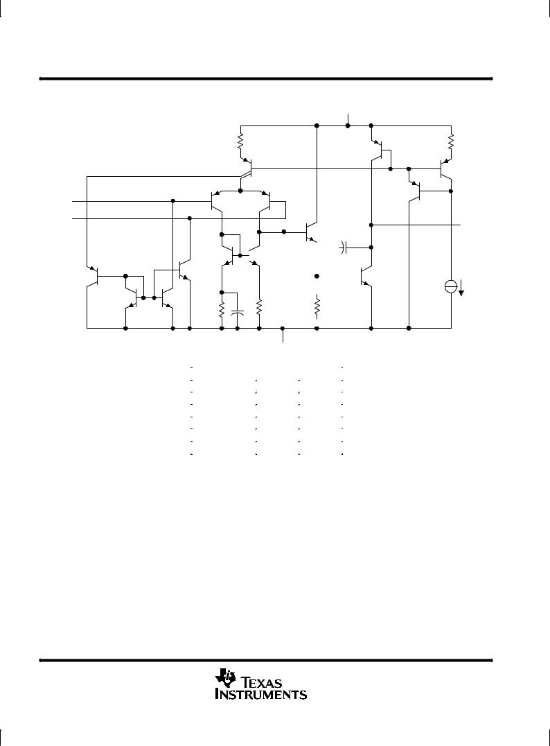
equivalent schematic (each amplifier)
VCC+
IN+
IN±
OUT
|
|
|
|
|
|
|
|
|
|
|
|
|
|
|
|
|
|
|
|
|
|
|
|
|
|
|
|
|
|
|
|
|
|
|
|
|
|
|
|
|
|
|
|
|
|
|
|
|
|
|
|
|
|
|
|
|
|
|
|
|
|
|
|
|
|
|
|
|
|
|
|
VCC± |
|
|
|
|
|
|
|
|
|
|
|
|
|
|
|
|
|
|
|
|
|
|
|
|
|
|
|
|
|
|
||
|
|
|
|
|
|
|
|
|
|
|
|
|
|
|
|
|
|
|
||
|
|
|
|
|
|
|
|
|
|
|
|
|
|
|
|
|
|
|
||
|
|
|
|
|
|
|
|
|
|
|
|
|
|
|
|
|
|
|
||
|
|
|
|
|
|
|
|
|
|
|
|
|
|
|
|
|
|
|
||
|
|
|
|
|
|
|
|
|
|
|
|
|
|
|
|
|
|
|
||
|
|
|
|
|
|
|
|
|
|
|
|
|
|
|
|
|
|
|
||
|
|
|
|
|
|
|
|
|
|
|
|
|
|
|
|
|
|
|
||
|
|
|
|
|
|
|
|
|
|
|
|
|
|
|
|
|
|
|
||
|
|
|
|
|
|
|
|
|||||||||||||
ACTUAL DEVICE COMPONENT COUNT |
|
|
|
|
||||||||||||||||
|
|
|
|
|
|
|
|
|
|
|||||||||||
COMPONENT |
|
|
TLV2361 |
TLV2362 |
|
|
|
|
||||||||||||
|
|
|
|
|
|
|
|
|
|
|||||||||||
Transistors |
|
30 |
|
46 |
|
|
|
|
||||||||||||
|
|
|
|
|
|
|
|
|
|
|||||||||||
Resistors |
|
6 |
|
11 |
|
|
|
|
||||||||||||
|
|
|
|
|
|
|
|
|
|
|||||||||||
Diodes |
|
1 |
|
1 |
|
|
|
|
||||||||||||
|
|
|
|
|
|
|
|
|
|
|||||||||||
Capacitors |
|
2 |
|
4 |
|
|
|
|
||||||||||||
|
|
|
|
|
|
|
|
|
|
|||||||||||
JFET |
|
1 |
|
1 |
|
|
|
|
||||||||||||
|
|
|
|
|
|
|
|
|
|
|
|
|
|
|
|
|
|
|
|
|
2 |
POST OFFICE BOX 655303 •DALLAS, TEXAS 75265 |
TLV2361, TLV2361Y, TLV2362, TLV2362Y
HIGH-PERFORMANCE LOW-VOLTAGE OPERATIONAL AMPLIFIERS
SLOS195B ± FEBRUARY 1997 ± REVISED OCTOBER 1998
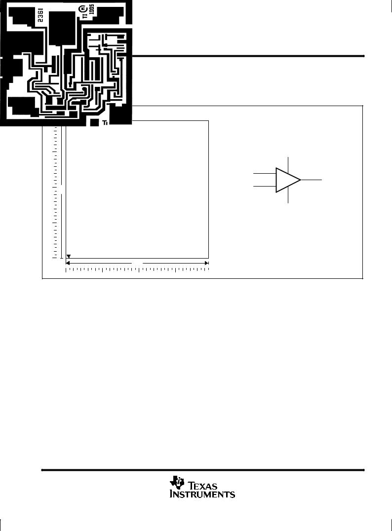
TLV2361Y chip information
This chip, when properly assembled, has characteristics similar to the TLV2361. Thermal compression or ultrasonic bonding can be used on the doped-aluminum bonding pads. This chip can be mounted with conductive epoxy or a gold-silicon preform.
|
Bonding-Pad Assignments |
|
|
|
(3) |
(4) |
|
|
|
|
|
|
VCC+ |
|
|
|
|
(5) |
|
|
|
(1) |
|
|
|
|
IN+ |
+ |
(4) |
|
|
(3) |
± |
OUT |
39 |
|
IN± |
|
|
|
|
|
|
|
(2) |
|
|
(2) |
|
|
|
|
|
|
|
|
|
VCC± |
|
|
|
Chip Thickness: 15 Mils Typical |
|
|
(1) |
|
Bonding Pads: 4 × 4 Mils Minimum |
|
|
|
(5) |
TJ(max) = 150°C |
|
|
|
Tolerances Are ±10%. |
|
|
|
|
|
All Dimensions Are in Mils. |
|
|
|
|
Pin (2) is Connected Internally to Backside of Chip. |
||
|
39 |
|
|
|
POST OFFICE BOX 655303 •DALLAS, TEXAS 75265 |
3 |

TLV2361, TLV2361Y, TLV2362, TLV2362Y
HIGH-PERFORMANCE LOW-VOLTAGE OPERATIONAL AMPLIFIERS
SLOS195B ± FEBRUARY 1997 ± REVISED OCTOBER 1998
TLV2362Y chip information
This chip, when properly assembled, has characteristics similar to the TLV2362. Thermal compression or ultrasonic bonding can be used on the doped-aluminum bonding pads. Chips can be mounted with conductive epoxy or a gold-silicon preform.
|
Bonding-Pad Assignments |
|
|
|
|
(1) |
(8) |
(7) |
|
VCC+ |
|
|
|
|
|
(8) |
|
|
|
|
(3) |
|
|
|
|
|
1IN+ |
+ |
(1) |
|
|
|
(2) |
± |
1OUT |
|
|
|
1IN± |
(5) |
|
|
|
|
|
|
|
|
|
|
(7) |
+ |
2IN+ |
|
|
|
2OUT |
± |
(6) |
39 |
|
|
|
2IN± |
|
|
|
|
|
|
|
(2) |
|
(6) |
|
(4) |
|
|
|
VCC± |
|
||
|
|
|
|
|
|
|
|
|
Chip Thickness: 15 Mils Typical |
|
|
|
|
|
Bonding Pads: 4 × 4 Mils Minimum |
|
|
(3) |
(4) |
(5) |
TJ(max) = 150°C |
|
|
|
|
Tolerances Are ±10%. |
|
||
|
|
|
All Dimensions Are in Mils. |
|
|
|
|
|
Pin (4) is Connected Internally to Backside of Chip. |
||
|
39 |
|
|
|
|
4 |
POST OFFICE BOX 655303 •DALLAS, TEXAS 75265 |

TLV2361, TLV2361Y, TLV2362, TLV2362Y
HIGH-PERFORMANCE LOW-VOLTAGE OPERATIONAL AMPLIFIERS
SLOS195B ± FEBRUARY 1997 ± REVISED OCTOBER 1998
absolute maximum ratings over operating free-air temperature range (unless otherwise noted)²
Supply voltage, VCC+ (see Note 1) . . . . . . . . . . . . . . . . . . . . . . . . . . . . . . . . . . . . . . . . . . . . . . . . . . |
. . . . . . . . 3.5 V |
Supply voltage, VCC± (see Note 1) . . . . . . . . . . . . . . . . . . . . . . . . . . . . . . . . . . . . . . . . . . . . . . . . . . |
. . . . . . . ±3.5 V |
Differential input voltage, VID (see Note 2) . . . . . . . . . . . . . . . . . . . . . . . . . . . . . . . . . . . . . . . . . . . |
. . . . . . . ±3.5 V |
Input voltage, VI (any input) (see Notes 1 and 3) . . . . . . . . . . . . . . . . . . . . . . . . . . . . . . . . . . . . . . |
. . . . . . . . VCC± |
Output voltage, VO . . . . . . . . . . . . . . . . . . . . . . . . . . . . . . . . . . . . . . . . . . . . . . . . . . . . . . . . . . . . . . . . |
. . . . . . . ±3.5 V |
Output current, IO . . . . . . . . . . . . . . . . . . . . . . . . . . . . . . . . . . . . . . . . . . . . . . . . . . . . . . . . . . . . . . . . . |
. . . . . . . 20 mA |
Duration of short-circuit current at (or below) 25°C (output shorted to GND) . . . . . . . . . . . . . . |
. . . . . Unlimited |
Package thermal impedance, θJA (see Note 4): D package . . . . . . . . . . . . . . . . . . . . . . . . . . . . . |
. . . . . 197°C/W |
DBV package . . . . . . . . . . . . . . . . . . . . . . . . . . |
. . . . . 347°C/W |
P package . . . . . . . . . . . . . . . . . . . . . . . . . . . . . |
. . . . . 104°C/W |
PW package . . . . . . . . . . . . . . . . . . . . . . . . . . . |
. . . . . 243°C/W |
Storage temperature range, Tstg . . . . . . . . . . . . . . . . . . . . . . . . . . . . . . . . . . . . . . . . . . . . . . . . . . . |
±65°C to 150°C |
Lead temperature 1,6 mm (1/16 inch) from case for 10 seconds . . . . . . . . . . . . . . . . . . . . . . . . |
. . . . . . . 260°C |
²Stresses beyond those listed under ªabsolute maximum ratingsº may cause permanent damage to the device. These are stress ratings only, and functional operation of the device at these or any other conditions beyond those indicated under ªrecommended operating conditionsº is not
implied. Exposure to absolute-maximum-rated conditions for extended periods may affect device reliability.
NOTES: 1. All voltage values, except differential voltages, are with respect to the midpoint between VCC+ and VCC±.
2.Differential voltages are at IN+ with respect to IN±.
3.All input voltage values must not exceed VCC.
4.The package thermal impedance is calculated in accordance with JESD 51, except for through-hole packages, which use a trace length of zero.
recommended operating conditions
|
C SUFFIX |
I SUFFIX |
UNIT |
||
|
|
|
|
|
|
|
MIN |
MAX |
MIN |
MAX |
|
|
|
||||
|
|
|
|
|
|
Supply voltage, VCC |
±1 |
±2.5 |
±1 |
±2.5 |
V |
Operating free-air temperature, TA |
0 |
70 |
±40 |
85 |
°C |
POST OFFICE BOX 655303 •DALLAS, TEXAS 75265 |
5 |
TLV2361, TLV2361Y, TLV2362, TLV2362Y
HIGH-PERFORMANCE LOW-VOLTAGE OPERATIONAL AMPLIFIERS
SLOS195B ± FEBRUARY 1997 ± REVISED OCTOBER 1998
TLV2361C electrical characteristics, VCC± = ±1.5 V (unless otherwise noted)
|
PARAMETER |
TEST CONDITIONS |
TA |
TLV2361C |
|
UNIT |
||
|
|
|
|
|||||
|
MIN |
TYP |
MAX |
|||||
|
|
|
|
|
|
|||
|
|
|
|
|
|
|
|
|
VIO |
Input offset voltage |
VO = 0, |
VIC = 0 |
25°C |
|
1 |
6 |
mV |
|
|
|
|
|||||
0°C to 70°C |
|
|
7.5 |
|||||
|
|
|
|
|
|
|
||
|
|
|
|
|
|
|
|
|
IIO |
Input offset current |
VO = 0, |
VIC = 0 |
25°C |
|
5 |
100 |
nA |
|
|
|
|
|||||
0°C to 70°C |
|
|
150 |
|||||
|
|
|
|
|
|
|
||
|
|
|
|
|
|
|
|
|
IIB |
Input bias current |
VO = 0, |
VIC = 0 |
25°C |
|
20 |
150 |
nA |
|
|
|
|
|||||
0°C to 70°C |
|
|
250 |
|||||
|
|
|
|
|
|
|
||
|
|
|
|
|
|
|
|
|
VIC |
Common-mode input voltage |
|VIO| ≤ 7.5 mV |
|
25°C |
±0.5 |
|
|
V |
|
|
|
|
|
||||
|
0°C to 70°C |
±0.5 |
|
|
||||
|
|
|
|
|
|
|
||
|
|
|
|
|
|
|
|
|
VOM+ |
Maximum positive-peak output voltage |
RL = 10 kΩ |
|
25°C |
1.2 |
1.4 |
|
V |
RL ≥ 10 kΩ |
|
0°C to 70°C |
1.2 |
|
|
|||
|
|
|
|
|
|
|||
VOM± |
Maximum negative-peak output voltage |
RL = 10 kΩ |
|
25°C |
±1.2 |
±1.4 |
|
V |
RL ≥ 10 kΩ |
|
0°C to 70°C |
±1.2 |
|
|
|||
|
|
|
|
|
|
|||
ICC |
Supply current (package) |
VO = 0, |
No load |
25°C |
|
1.4 |
2.25 |
mA |
|
|
|
|
|||||
0°C to 70°C |
|
|
2.75 |
|||||
|
|
|
|
|
|
|
||
|
|
|
|
|
|
|
|
|
AVD |
Large-signal differential voltage amplification |
VO = ±1 V, |
RL = 10 kΩ |
25°C |
60 |
80 |
|
dB |
CMRR |
Common-mode rejection ratio |
VIC = ±0.5 V |
|
25°C |
|
75 |
|
dB |
kSVR |
Supply-voltage rejection ratio |
VCC± = ±1.5 V to ±2.5 V |
25°C |
|
80 |
|
dB |
|
TLV2361C operating characteristics, VCC± = ±1.5 V, TA = 25°C
|
PARAMETER |
|
TEST CONDITIONS |
TLV2361C |
|
UNIT |
||||
|
|
|
|
|
||||||
|
|
MIN |
TYP |
MAX |
||||||
|
|
|
|
|
|
|
|
|||
|
|
|
|
|
|
|
|
|
|
|
SR |
Slew rate |
AV = 1, |
VI = ±0.5 V |
|
|
2.5 |
|
V/μs |
||
B1 |
Unity-gain bandwidth |
AV = 40, |
RL = 10 kΩ, |
CL = 100 pF |
|
6 |
|
MHz |
||
|
|
RS = 100 Ω, |
RF = 10 kΩ, |
|
|
|
|
|
||
Vn |
Equivalent input noise voltage |
f = 1 kHz |
|
9 |
|
nV/√ |
Hz |
|
||
6 |
POST OFFICE BOX 655303 •DALLAS, TEXAS 75265 |
 Loading...