


 Loading...
TEXAS INSTRUMENTS TLV320AIC20, TLV320AIC21, TLV320AIC24, TLV320AIC25, TLV320AIC20K Technical data
...TLV320AIC20, TLV320AIC21
TLV320AIC24, TLV320AIC25
TLV320AIC20K, TLV320AIC24K
www.ti.com |
SLAS363D –MARCH 2002 –REVISED APRIL 2005 |
|
Low-Power, Highly-Integrated, Programmable
16-Bit, 26-KSPS, Dual-Channel CODEC
FEATURES
∙Stereo 16-Bit Oversampling Sigma-Delta A/D Converter
∙Stereo 16-Bit Oversampling Sigma-Delta D/A Converter
∙Support Maximum Master Clock of 100 MHz to Allow DSPs Output Clock to be Used as a Master Clock
∙Selectable FIR/IIR Filter With Bypassing Option
∙Programmable Sampling Rate up to:
–Max 26 Ksps With On-Chip IIR/FIR Filter
–Max 104 Ksps With IIR/FIR Bypassed
∙On-Chip FIR Produced 84-dB SNR for ADC and 92-dB SNR for DAC over 13-Khz BW
∙Smart Time Division Multiplexed (SMARTDM® ) Serial Port
–Glueless 4-Wire Interface to DSP
–Automatic Cascade Detection (ACD) Self-Generates Master/Slave Device Addresses
–Programming Mode to Allow On-The-Fly Reconfiguration
–Continuous Data Transfer Mode to Minimize Bit Clock Speed
–Support Different Sampling Rate for Each Device
–Turbo Mode to Maximize Bit Clock For Faster Data Transfer and Allow Multiple Serial Devices to Share the Same Bus
–Allows up to Eight Devices to be Connected to a Single Serial Port
∙Host port
–2-Wire Interface
–Selectable I2C or S2C
∙Differential and Single-Ended Analog Input/Output
∙Built-In Analog Functions:
–Analog and Digital Sidetone
–Antialiasing Filter (AAF)
–Programmable Input and Output Gain Control (PGA)
–Microphone/Handset/Headset Amplifiers
–AIC20/21/20K Have a Built-In 8-Ω Speaker
Driver
–Power Management With Hardware/Software Power-Down Modes 30 µW
∙Separate Software Control for ADC and DAC Power Down
∙Fully Compatible With Common TMS320® DSP Family and Microcontroller Power Supplies
–1.65-V - 1.95-V Digital Core Power
–1.1-V - 3.6-V Digital I/O
–2.7-V - 3.6-V Analog
∙Internal Reference Voltage (Vref)
∙2s Complement Data Format
∙Test Mode Which Includes Digital Loopback and Analog Loopback
APPLICATIONS
∙Wireless Accessories
∙Hands-Free Car Kits
∙VOIP
∙Cable Modem
∙Speech Processing
Please be aware that an important notice concerning availability, standard warranty, and use in critical applications of Texas Instruments semiconductor products and disclaimers thereto appears at the end of this data sheet.
SMARTDM, TMS320, TMS320C5000, TMS320C6000 are registered trademarks of Texas Instruments.
PRODUCTION DATA information is current as of publication date. |
Copyright © 2002–2005, Texas Instruments Incorporated |
Products conform to specifications per the terms of the Texas |
|
Instruments standard warranty. Production processing does not |
|
necessarily include testing of all parameters. |
|

TLV320AIC20, TLV320AIC21
TLV320AIC24, TLV320AIC25
TLV320AIC20K, TLV320AIC24K
www.ti.com
SLAS363D –MARCH 2002 –REVISED APRIL 2005
These devices have limited built-in ESD protection. The leads should be shorted together or the device placed in conductive foam during storage or handling to prevent electrostatic damage to the MOS gates.
DESCRIPTION
The TLV320AIC2x is a low-cost, low-power, highly-integrated, high-performance, dual-voice codec. It features two 16-bit analog-to-digital (A/D) channels and two 16-bit digital-to-analog (D/A) channels, which can be connected to a handset, headset, speaker, microphone, or a subscriber line via a programmable analog crosspoint.
The TLV320AIC2x provides high resolution signal conversion from digital-to-analog (D/A) and from analog-to-digital (A/D) using oversampling sigma-delta technology with programmable sampling rate.
The TLV320AIC2x implements the smart time division multiplexed serial port (SMARTDM™) . The SMARTDM port is a synchronous 4-wire serial port in TDM format for glue-free interface to TI DSPs (i.e., TMS320C5000® , TMS320C6000® DSP platforms) and microcontrollers. The SMARTDM™ supports both continuous data transfer mode and on-the-fly reconfiguration programming mode. The TLV320AIC2x can be gluelessly cascaded to any SMARTDM-based device to form a multichannel codec, and up to eight TLV320AIC2x codecs can be cascaded to a single serial port.
The TLV320AIC2x provides a flexible host port. The host port interface is a two-wire serial interface that can be programmed to be either an industrial standard I2C or a simple S2C (start-stop communication protocol).
The TLV320AIC2x integrates all of the critical functions needed for most voice-band applications including MIC preamplifier, handset amplifier headset amplifier, 8-Ω speaker driver, sidetone control, antialiasing filter (AAF), input/output programmable gain amplifier (PGA), and selectable low-pass IIR/FIR filters.
The TLV320AIC2x implements an extensive power management; including device power-down, independent software control for turning off ADC, DAC, operational-amplifiers, and IIR/FIR filter (bypassable) to maximize system power conservation. The TLV320AIC2x consumes only 14.9 mW per channel at 3 V.
The TLV320AIC2x low power operation from 2.7-V to 3.6-V power supplies along with extensive power management make it ideal for portable applications including wireless accessories, hands-free car kits, VOIP, cable modem, and speech processing. Its low group delay characteristic makes it suitable for single or multichannel active control applications.
The TLV320AIC2x is characterized for commercial operation from 0°C to 70°C, and industrial operation from -40°C to 85°C. The TLV320AIC2xk is characterized for industrial operation from -40°C to 85°C.
|
ORDERING INFORMATION |
T |
48-TQFP PFB PACKAGE(1) |
A |
|
0°C to 70°C |
TLV320AIC2xC |
-40°C to 85°C |
TLV320AIC2xI |
(1)For the most current package and ordering information, see the Package Option Addendum at the end of this document, or see the TI website at www.ti.com.
2
|
|
|
|
|
|
|
|
|
|
|
|
|
|
|
|
|
|
|
|
|
|
|
|
|
|
|
|
|
|
|
|
|
|
|
|
TLV320AIC20, TLV320AIC21 |
||||
|
|
|
|
|
|
|
|
|
|
|
|
|
|
|
|
|
|
|
|
|
|
|
|
|
|
|
|
|
|
|
|
|
|
|
|
TLV320AIC24, TLV320AIC25 |
||||
www.ti.com |
|
|
|
|
|
|
|
|
|
|
|
|
|
|
|
|
|
|
|
|
|
|
|
|
|
|
|
|
|
|
|
|
|
|
TLV320AIC20K, TLV320AIC24K |
|||||
|
|
|
|
|
|
|
|
|
|
|
|
|
|
|
|
|
|
|
|
|
|
|
|
|
|
|
|
|
|
|
|
|
SLAS363D –MARCH 2002 –REVISED APRIL 2005 |
|||||||
|
|
|
|
|
|
|
|
|
|
|
|
|
|
|
|
|
|
|
|
|
|
|
|
|
|
|
|
|
|
|
|
|
|
|||||||
|
|
|
|
|
|
|
|
|
|
|
|
|
|
|
|
|
|
PFB |
|
|
|
|
|
|
|
|
|
|
|
|
|
|
|
|
|
|
|
|
||
|
|
|
|
|
|
|
|
|
|
|
|
|
|
|
|
|
TOP VIEW |
|
|
|
|
|
|
|
|
|
|
|
|
|
|
|
|
|
||||||
|
|
|
|
MICBIAS |
MICI+ |
MICI- |
|
AVDD1 |
AVSS1 |
CIDI+ |
|
CIDI- |
DRVSS2 |
|
SPKO- |
|
DRVDD |
|
SPKO+ |
|
DRVSS1 |
|
|
|||||||||||||||||
|
|
|
|
|
|
|
|
|
|
|
|
|
|
|
|
|
|
|
|
|
|
|
|
|
|
|
|
|
|
|
|
|
|
|
|
|
|
|
|
|
|
|
|
36 |
35 |
34 |
33 |
32 |
31 |
30 |
29 |
28 |
27 |
26 |
25 |
|
|
|
|
|
|||||||||||||||||||||
|
LCDAC |
|
37 |
|
|
|
|
|
|
|
|
|
|
|
|
|
|
|
|
|
|
|
|
|
|
|
|
|
|
|
|
24 |
|
|
VSS |
|||||
|
|
|
|
|
|
|
|
|
|
|
|
|
|
|
|
|
|
|
|
|
|
|
|
|
|
|
|
|
|
|
|
|||||||||
|
|
|
|
|
|
|
|
|
|
|
|
|
|
|
|
|
|
|
|
|
|
|
|
|
|
|
|
|
|
|
|
|
|
|
|
|
|
|
|
|
|
HNSO- |
|
38 |
|
|
|
|
|
|
|
|
|
|
|
|
|
|
|
|
|
|
|
|
|
|
|
|
|
|
|
|
23 |
|
|
RESET |
|||||
|
|
|
|
|
|
|
|
|
|
|
|
|
|
|
|
|
|
|
|
|
|
|
|
|
|
|
|
|
|
|
|
|||||||||
|
HNSO+ |
|
39 |
|
|
|
|
|
|
|
|
|
|
|
|
|
|
|
|
|
|
|
|
|
|
|
|
|
|
|
|
22 |
|
|
MCLK |
|||||
|
|
|
|
|
|
|
|
|
|
|
|
|
|
|
|
|
|
|
|
|
|
|
|
|
|
|
|
|
|
|
|
|||||||||
|
HNSI- |
|
40 |
|
|
|
|
|
|
|
|
|
|
|
|
|
|
|
|
|
|
|
|
|
|
|
|
|
|
|
|
21 |
|
|
M/S |
|||||
|
|
|
|
|
|
|
|
|
|
|
|
|
|
|
|
|
|
|
|
|
|
|
|
|
|
|
|
|
|
|
|
|||||||||
|
HNSI+ |
|
41 |
|
|
|
|
|
|
|
|
|
|
|
|
|
|
|
|
|
|
|
|
|
|
|
|
|
|
|
|
20 |
|
|
SCLK |
|||||
|
|
|
|
|
|
|
|
|
|
|
|
|
|
|
|
|
|
|
|
|
|
|
|
|
|
|
|
|
|
|
|
|||||||||
|
AVDD |
|
42 |
|
|
|
|
|
|
|
|
|
|
|
|
|
|
|
|
|
|
|
|
|
|
|
|
|
|
|
|
19 |
|
|
FS |
|||||
|
|
|
|
|
|
|
|
|
|
|
|
|
|
|
|
|
|
|
|
|
|
|
|
|
|
|
|
|
|
|
|
|||||||||
|
AVSS |
|
43 |
|
|
|
|
|
|
|
|
|
|
|
|
|
|
|
|
|
|
|
|
|
|
|
|
|
|
|
|
18 |
|
|
DIN |
|||||
|
|
|
|
|
|
|
|
|
|
|
|
|
|
|
|
|
|
|
|
|
|
|
|
|
|
|
|
|
|
|
|
|||||||||
|
LINEI+ |
|
44 |
|
|
|
|
|
|
|
|
|
|
|
|
|
|
|
|
|
|
|
|
|
|
|
|
|
|
|
|
17 |
|
|
DOUT |
|||||
|
|
|
|
|
|
|
|
|
|
|
|
|
|
|
|
|
|
|
|
|
|
|
|
|
|
|
|
|
|
|
|
|||||||||
|
LINEI- |
|
45 |
|
|
|
|
|
|
|
|
|
|
|
|
|
|
|
|
|
|
|
|
|
|
|
|
|
|
|
|
16 |
|
|
DVSS |
|||||
|
|
|
|
|
|
|
|
|
|
|
|
|
|
|
|
|
|
|
|
|
|
|
|
|
|
|
|
|
|
|
|
|||||||||
|
LINEO- |
|
46 |
|
|
|
|
|
|
|
|
|
|
|
|
|
|
|
|
|
|
|
|
|
|
|
|
|
|
|
|
15 |
|
|
DVDD |
|||||
|
|
|
|
|
|
|
|
|
|
|
|
|
|
|
|
|
|
|
|
|
|
|
|
|
|
|
|
|
|
|
|
|||||||||
|
LINEO+ |
|
47 |
|
|
|
|
|
|
|
|
|
|
|
|
|
|
|
|
|
|
|
|
|
|
|
|
|
|
|
|
14 |
|
|
FSD |
|||||
|
|
|
|
|
|
|
|
|
|
|
|
|
|
|
|
|
|
|
|
|
|
|
|
|
|
|
|
|
|
|
|
|||||||||
|
NC |
|
48 |
|
|
|
|
|
|
|
|
|
|
|
|
|
|
|
|
|
|
|
|
|
|
|
|
|
|
|
|
13 |
|
|
IOVSS |
|||||
|
|
|
|
|
|
|
|
|
|
|
|
|
|
|
|
|
|
|
|
|
|
|
|
|
|
|
|
|
|
|
|
|||||||||
|
|
|
1 |
|
2 |
|
3 |
|
4 |
|
5 |
|
6 |
|
7 |
|
8 |
|
9 |
|
10 |
11 |
12 |
|
|
|
|
|
||||||||||||
|
|
|
|
|
|
|
||||||||||||||||||||||||||||||||||
|
|
|
|
|
|
|
|
|
|
|
|
|
|
|
|
|
|
|
|
|
|
|
|
|
|
|
|
|
|
|
|
|
|
|
|
|
|
|
|
|
|
|
|
|
|
|
|
|
|
|
|
|
|
|
|
|
|
|
|
|
|
|
|
|
|
|
|
|
|
|
|
|
|
|
|
|
|
|
|
|
|
|
|
|
|
|
HDSI- |
|
HDSI+ |
|
HDSO- |
|
HDSO+ |
|
AVDD2 |
AVSS2 |
|
TESTP |
NC |
|
PWRDN |
|
SDA |
|
SCL |
|
IOVDD |
|
|
|||||||||||||
|
|
|
|
|
|
|
|
|
|
|
|
|
|
|
|
|||||||||||||||||||||||||
|
|
|
|
|
|
|
|
|
|
|
|
|
Terminal Functions |
|
|
|
|
|
|
|
|
|
|
|
|
|||||||||||||||
TERMINAL |
|
|
|
|
|
|
|
|
|
|
|
|
|
|
|
|
|
|
|
|
|
|
|
|
|
|
|
|
|
|
|
|
|
|
|
|
|
|
|
|
NAME |
NO. |
|
I/O |
|
|
|
|
|
|
|
|
|
|
|
|
|
|
|
|
|
|
|
|
|
|
|
|
DESCRIPTION |
|
|
||||||||||
HDSI- |
1 |
|
|
|
I |
|
|
|
|
Head-set input. The Head-set input can be treated similar to the Line-input pins |
||||||||||||||||||||||||||||||
HDSI+ |
2 |
|
|
|
|
|
|
|
||||||||||||||||||||||||||||||||
|
|
|
|
|
|
|
|
|
|
|
|
|
|
|
|
|
|
|
|
|
|
|
|
|
|
|
|
|
|
|
|
|
|
|
|
|
|
|
||
HDSO- |
3 |
|
|
|
O |
|
|
|
|
150-Ω output |
|
|
|
|
|
|
|
|
|
|
|
|
|
|
|
|
|
|
|
|
|
|
||||||||
HDSO+ |
4 |
|
|
|
|
|
|
|
|
|
|
|
|
|
|
|
|
|
|
|
|
|
|
|
|
|
|
|
|
|
||||||||||
|
|
|
|
|
|
|
|
|
|
|
|
|
|
|
|
|
|
|
|
|
|
|
|
|
|
|
|
|
|
|
|
|
|
|
|
|
|
|
||
AVDD2 |
5 |
|
|
|
I |
|
|
|
|
Analog power supply |
|
|
|
|
|
|
|
|
|
|
|
|
|
|
|
|
|
|||||||||||||
AVSS2 |
6 |
|
|
|
I |
|
|
|
|
Analog ground |
|
|
|
|
|
|
|
|
|
|
|
|
|
|
|
|
|
|
|
|
||||||||||
TESTP |
7 |
|
|
|
I |
|
|
|
|
Test pin. Should be connected to digital ground. |
|
|
||||||||||||||||||||||||||||
NC |
8, 48 |
|
|
|
|
|
|
|
|
|
Not connected |
|
|
|
|
|
|
|
|
|
|
|
|
|
|
|
|
|
|
|
|
|||||||||
PWRDN |
9 |
|
|
|
I |
|
|
|
|
Power down |
|
|
|
|
|
|
|
|
|
|
|
|
|
|
|
|
|
|
|
|
|
|
||||||||
SDA |
10 |
|
|
I/O |
|
|
|
|
I2C/S2C data |
|
|
|
|
|
|
|
|
|
|
|
|
|
|
|
|
|
|
|
|
|
|
|||||||||
SCL |
11 |
|
|
|
I |
|
|
|
|
I2C/S2C clock |
|
|
|
|
|
|
|
|
|
|
|
|
|
|
|
|
|
|
|
|
||||||||||
IOVDD |
12 |
|
|
|
I |
|
|
|
|
I/O power supply |
|
|
|
|
|
|
|
|
|
|
|
|
|
|
|
|
|
|
|
|
||||||||||
IOVSS |
13 |
|
|
|
I |
|
|
|
|
I/O ground |
|
|
|
|
|
|
|
|
|
|
|
|
|
|
|
|
|
|
|
|
|
|
||||||||
FSD |
14 |
|
|
|
O |
|
|
|
|
Frame sync delayed |
|
|
|
|
|
|
|
|
|
|
|
|
|
|
|
|
|
|||||||||||||
DVDD |
15 |
|
|
|
I |
|
|
|
|
Digital supply (1.8 V) |
|
|
|
|
|
|
|
|
|
|
|
|
|
|
|
|
|
|||||||||||||
DVSS |
16 |
|
|
|
I |
|
|
|
|
Digital ground |
|
|
|
|
|
|
|
|
|
|
|
|
|
|
|
|
|
|
|
|
||||||||||
DOUT |
17 |
|
|
|
O |
|
|
|
|
Data OUT |
|
|
|
|
|
|
|
|
|
|
|
|
|
|
|
|
|
|
|
|
|
|
||||||||
DIN |
18 |
|
|
|
I |
|
|
|
|
Data IN |
|
|
|
|
|
|
|
|
|
|
|
|
|
|
|
|
|
|
|
|
|
|
|
|
|
|||||
FS |
19 |
|
|
I/O |
|
|
|
|
Frame sync |
|
|
|
|
|
|
|
|
|
|
|
|
|
|
|
|
|
|
|
|
|
|
|||||||||
SCLK |
20 |
|
|
I/O |
|
|
|
|
Serial clock |
|
|
|
|
|
|
|
|
|
|
|
|
|
|
|
|
|
|
|
|
|
|
|||||||||
3
TLV320AIC20, TLV320AIC21
TLV320AIC24, TLV320AIC25
TLV320AIC20K, TLV320AIC24K
www.ti.com
SLAS363D –MARCH 2002 –REVISED APRIL 2005
TERMINAL |
|
NAME |
NO. |
M/S |
21 |
MCLK |
22 |
RESET |
23 |
VSS |
24 |
DRVSS1 |
25 |
SPKO+ |
26 |
SPKO- |
28 |
DRVDD |
27 |
DRVSS2 |
29 |
CIDI- |
30 |
CIDI+ |
31 |
AVDD1 |
33 |
AVSS1 |
32 |
MICI- |
34 |
MICI+ |
35 |
MICBIAS |
36 |
LCDAC |
37 |
HNSO- |
38 |
HNSO+ |
39 |
HNSI- |
40 |
HNSI+ |
41 |
AVDD |
42 |
AVSS |
43 |
LINEI+ |
44 |
LINEI- |
45 |
LINEO- |
46 |
LINEO+ |
47 |
|
Terminal Functions (continued) |
I/O |
DESCRIPTION |
I |
Master slave select applied to CODEC1 only. CODEC2 is always a slave. |
I |
Master clock |
I |
Reset |
I |
Device ground. Typically this should be connected to the Analog Ground. |
I |
Driver ground |
O |
8-Ω output |
I |
Driver supply |
I |
Driver ground |
I |
Caller-ID input. The Caller-ID input can be treated similar to the Line-input pins |
I |
Analog supply |
I |
Analog ground |
I |
Microphone input |
I |
Microphone input |
I |
Microphone bias |
O |
6-Bit DAC output may be used to drive LCDAC |
O |
150-Ω output |
I |
Hand-set input. The Hand-set input can be treated similar to the Line-input pins |
I |
Analog supply |
I |
Analog ground |
I |
Line input |
O |
600-Ω output |
4

TLV320AIC20, TLV320AIC21
TLV320AIC24, TLV320AIC25
TLV320AIC20K, TLV320AIC24K
www.ti.com
SLAS363D –MARCH 2002 –REVISED APRIL 2005
Electrical Characteristics
All specifications are common across the AIC20, AIC21, AIC24, AIC25, AIC20K, and AIC24K except where explicitly stated.
AIC20/21/24/25: Over Recommended Operating Free-Air Temperature Range, AVDD = 3.3 V, DVDD = 1.8 V, IOVDD = 3.3 V (Unless Otherwise Noted)
AIC20K/24K: Over Recommended Operating Free-Air Temperature Range, AVDD = 3.3 V, DVDD = 1.8 V, IOVDD = 3.3 V (Unless Otherwise Noted)
Absolute Maximum Ratings(1)
over Operating Free-Air Temperature Range (Unless Otherwise Noted)
|
|
|
TLV320AIC2x |
V |
Supply voltage range: |
DVDD(2) |
-0.3 V to 2.25 V |
CC |
|
|
|
|
|
AVDD, IOVDD, DRVDD(2) |
-0.3 V to 4 V |
VO |
Output voltage range, all digital output signals |
-0.3 V to IOVDD + 0.3 V |
|
VI |
Input voltage range, all digital input signals |
|
-0.3 V to IOVDD + 0.3 V |
TA |
Operating free-air temperature range |
|
-40°C to 85°C |
Tstg |
Storage temperature range |
|
-65°C to 150°C |
|
Case temperature for 10 seconds: package |
|
260°C |
(1)Stresses beyond those listed under absolute maximum ratings may cause permanent damage to the device. These are stress ratings only and functional operation of the device at these or any other conditions beyond those indicated under recommended operating conditions is not implied. Exposure to absolute-maximum-rated conditions for extended periods may affect device reliability.
(2)All voltage values are with respect to VSS.
Recommended Operating Conditions
|
|
MIN |
NOM |
MAX |
UNIT |
|
Analog, AVDD |
2.7 |
3.3 |
3.6 |
V |
VCC |
Analog output driver, DRVDD(1) |
2.7 |
3.3 |
3.6 |
V |
Supply voltage |
1.65 |
1.8 |
1.95 |
V |
|
|
Digital core, DVDD |
||||
|
Digital I/O, IOVDD |
1.1 |
3.3 |
3.6 |
V |
|
Analog single-ended peak-to-peak input voltage, VI(analog) |
|
|
2 |
V |
|
Between LINEO+ and LINEO- (differential) |
|
600 |
|
|
RL |
Between HDSO+ and HDSO- (differential) |
|
150 |
|
Ω |
Output load resistance, |
|
150 |
|
||
|
Between HNSO+ and HDSO- (differential) |
|
|
|
|
|
Between SPKO+ and SPKO- (differential) |
|
8 |
|
|
CL |
Analog output load capacitance |
|
|
20 |
pF |
|
Digital output capacitance |
|
|
20 |
pF |
|
Master clock |
|
|
100 |
MHz |
|
ADC or DAC conversion rate |
|
|
26 |
kHz |
TA |
Operating free-air temperature, |
-40 |
|
85 |
°C |
(1)DRVDD should be kept at the same voltage as AVDD.
5
TLV320AIC20, TLV320AIC21 |
|
|
|
|
|
TLV320AIC24, TLV320AIC25 |
|
|
|
|
|
TLV320AIC20K, TLV320AIC24K |
|
|
www.ti.com |
||
SLAS363D –MARCH 2002 –REVISED APRIL 2005 |
|
|
|||
|
|
|
|
||
Digital Inputs and Outputs |
|
|
|
|
|
FS = 8 KHz, outputs not loaded |
|
|
|
|
|
|
PARAMETER |
MIN |
TYP |
MAX |
UNIT |
VOH |
High-level output voltage, DOUT |
0.8 IOVDD |
|
|
V |
VOL |
Low-level output voltage, DOUT |
|
|
0.1 IOVDD |
V |
IIH |
High-level input current, any digital input |
|
5 |
|
µA |
IIL |
Low-level input current, any digital input |
|
5 |
|
µA |
Ci |
Input capacitance |
|
3 |
|
pF |
Co |
Output capacitance |
|
5 |
|
pF |
ADC PATH FILTER
FS = 8 KHz (1)(2)
PARAMETER
 PATH FILTER
Filter gain relative to gain at 1020 Hz
TEST |
MIN |
TYP |
MAX |
MIN |
TYP |
MAX |
UNIT |
|
CONDITIONS |
||||||||
|
|
|
|
|
|
|
||
|
|
FIR FILTER |
|
IIR FILTER |
|
|||
0 Hz to 60 Hz |
|
|
-27 / 0.07 |
|
|
-27 / 0.15 |
|
|
60 Hz to 200 Hz |
|
|
-1 / 0.07 |
|
|
-0.75 / 0.15 |
|
|
200 Hz to 300 Hz |
|
|
-0.03 / 0.05 |
|
|
0. 11 / 0.15 |
|
|
300 Hz to 2.4 KHz |
-0.1 |
|
0.15 |
-0.1 |
|
0.25 |
|
|
2.4 kHz to 3 kHz |
-0.05 |
|
0.15 |
-0.5 |
|
0.2 |
dB |
|
3 kHz to 3.4 KHz |
-0.5 |
|
0.1 |
-0.5 |
|
0.2 |
|
|
3.4 kHz to 3.6 KHz |
|
|
-0.4 |
|
|
0.15 |
|
|
4 KHz |
|
|
-26 |
|
|
-42 |
|
|
4.5 KHz to 72 kHz |
|
|
-52 |
|
|
-52 |
|
|
(1)The filter gain outside of the passband is measured with respect to the gain at 1020 Hz. The analog input test signal is a sine wave with
0 dB = 4 VI(PP) as the reference level for the analog input signal. The pass band is 0 to 3600 Hz for an 8-KHz sample rate. This pass band scales linearly with the sample rate.
(2)The filter characteristics are specified by design and are not tested in production. In places where more than one value is specified, the first value is with the High Pass Filter on and the second value is with the HPF off
ADC DYNAMIC PERFORMANCE
With FIR Filter, FS = 8 KHz (1)
|
PARAMETER |
TEST |
MIN |
TYP |
MAX |
MIN |
TYP |
MAX UNIT |
|
CONDITIONS |
|||||||
|
|
|
|
|
|
|
|
|
Line In Driver |
|
|
AIC20/21/24/25 |
|
|
AIC20k/24k |
|
|
SNR |
Signal-to-noise ratio |
VI = -3 dB |
81 |
84 |
|
70 |
84 |
|
VI = -9 dB |
73 |
76 |
|
|
76 |
|
||
|
|
|
|
|
||||
THD |
Total harmonic distortion |
VI = -3 dB |
83 |
90 |
|
70 |
90 |
dB |
VI = -9 dB |
81 |
88 |
|
|
88 |
|||
|
|
|
|
|
||||
THD+N |
Signal-to-harmonic |
VI = -3 dB |
80 |
83 |
|
|
83 |
|
distortion + noise |
VI = -9 dB |
73 |
76 |
|
|
76 |
|
|
|
|
|
|
|||||
(1)The test condition is a differential 1020-Hz input signal with an 8-KHz conversion rate. Input and output common mode is 1.35 V.
6

|
|
|
|
|
|
|
|
TLV320AIC20, TLV320AIC21 |
|||
|
|
|
|
|
|
|
|
TLV320AIC24, TLV320AIC25 |
|||
www.ti.com |
|
|
|
|
|
TLV320AIC20K, TLV320AIC24K |
|||||
|
|
|
|
|
SLAS363D –MARCH 2002 –REVISED APRIL 2005 |
||||||
|
|
|
|
|
|
|
|||||
ADC DYNAMIC PERFORMANCE |
|
|
|
|
|
|
|
|
|
||
With IIR Filter, FS = 8 KHz |
|
|
|
|
|
|
|
|
|
|
|
|
PARAMETER |
TEST |
|
MIN |
TYP |
MAX |
MIN |
TYP |
MAX |
UNIT |
|
|
CONDITIONS |
|
|||||||||
|
|
|
|
|
|
|
|
|
|
|
|
|
|
|
|
|
AIC20/21/24/25 |
|
AIC20k/24k |
|
|
||
SNR |
Signal-to-noise ratio |
VI = -3 dB |
|
|
82 |
|
|
|
82 |
|
|
VI = -9 dB |
|
|
76 |
|
|
|
76 |
|
|
||
|
|
|
|
|
|
|
|
|
|||
THD |
Total harmonic distortion |
VI = -3 dB |
|
|
83 |
|
|
|
83 |
|
dB |
VI = -9 dB |
|
|
77 |
|
|
|
77 |
|
|||
|
|
|
|
|
|
|
|
|
|||
THD+N |
Signal-to-harmonic |
VI = -3 dB |
|
|
78 |
|
|
|
78 |
|
|
distortion + noise |
VI = -9 dB |
|
|
70 |
|
|
|
70 |
|
|
|
|
|
|
|
|
|
|
|
||||
ADC CHANNEL CHARACTERISTICS |
|
|
|
|
|
|
|
|
|
||
|
PARAMETER |
|
TEST CONDITIONS |
|
AIC20/21/24/25/20k/24k |
|
|
||||
|
|
|
MIN |
TYP |
MAX |
UNIT |
|||||
|
|
|
|
|
|
|
|||||
VI(pp) |
Differential-ended input level |
|
|
PGA gain = 0 dB |
|
|
|
|
4 |
V |
|
VIO |
Input offset voltage |
|
|
|
|
|
|
|
±5 |
|
mV |
IB |
Input bias current |
|
|
|
|
|
|
125 |
|
µA |
|
|
Common mode voltage |
|
|
|
|
|
|
1.35 |
|
V |
|
|
Dynamic range |
|
|
VI = -3 dB |
|
|
|
87 |
|
dB |
|
|
Mute attenuation |
|
|
PGA = MUTE |
|
|
Zero Digital |
|
dB |
||
|
|
|
|
|
Code |
|
|||||
|
|
|
|
|
|
|
|
|
|
||
|
Intrachannel isolation |
|
|
|
|
|
|
|
87 |
|
dB |
EG |
Gain error |
|
VI = -3 dB at 1020 Hz |
|
|
-0.45 |
|
dB |
|||
EO(ADC) |
ADC converter offset error |
|
|
|
|
|
|
|
±15 |
|
mV |
CMRR |
Common-mode rejection ratio at INMx and |
VI = -100 mV at 1020 Hz |
|
|
|
50 |
|
dB |
|||
INPx |
|
|
|
|
|
||||||
|
Idle channel noise |
|
V(INP,INM,MICIN) = 0 V |
|
|
|
70 |
|
µVrms |
||
Ri |
Input resistance |
|
|
TA = 25°C |
|
|
|
10 |
|
kΩ |
|
Ci |
Input capacitance |
|
|
TA = 25°C |
|
|
|
2 |
|
pF |
|
|
Channel delay |
|
|
|
IIR |
|
|
|
5/fs |
|
S |
|
|
|
|
FIR |
|
|
17/fs |
|
S |
||
|
|
|
|
|
|
|
|
||||
DAC PATH FILTER |
|
|
|
|
|
|
|
|
|
|
|
FS = 8 KHz (1)(2) |
|
|
|
|
|
|
|
|
|
|
|
|
PARAMETER |
TEST CONDITIONS |
FIR FILTER |
|
|
IIR FILTER |
|
||||
|
MIN |
TYP |
MAX |
MIN |
TYP |
MAX |
UNIT |
||||
|
|
|
|
|
|||||||
PATH FILTER, FS = 8 KHz |
|
|
|
|
|
|
|
|
|
|
|
|
|
0 Hz to 200 Hz |
|
|
|
0.1 |
|
|
0.05 |
|
|
|
|
200 Hz to 300 Hz |
|
|
|
-0.05 |
|
|
0.05 |
|
|
|
|
300 Hz to 2.4 KHz |
|
-0.25 |
|
0.15 |
-0.1 |
|
0.1 |
|
|
Filter gain relative to gain |
2.4 kHz to 3 kHz |
|
-0.3 |
|
0.1 |
-0.2 |
|
0.1 |
dB |
||
|
at 1020 Hz |
3 kHz to 3.4 KHz |
|
-0.55 |
|
0.05 |
-0.25 |
|
0.05 |
||
|
|
|
|
|
|||||||
|
|
3.4 kHz to 3.6 KHz |
|
|
|
-30 |
|
|
0 |
|
|
|
|
4 KHz |
|
|
|
|
-28 |
|
|
-34 |
|
|
|
4.5 KHz to 72 KHZ |
|
|
|
-70 |
|
|
-70 |
|
|
(1)The filter gain outside of the passband is measured with respect to the gain at 1020 Hz. The input signal is the digital equivalent of a
sine wave (digital full scale = 0 dB). The nominal differential DAC channel output with this input condition is 4 VI(PP) . The pass band is 0 to 3600 Hz for an 8-kHz sample rate. This pass band scales linearly with the conversion rate.
(2)The filter characteristics are specified by design and are not tested in production.
7
TLV320AIC20, TLV320AIC21
TLV320AIC24, TLV320AIC25
TLV320AIC20K, TLV320AIC24K
www.ti.com
SLAS363D –MARCH 2002 –REVISED APRIL 2005
DAC DYNAMIC PERFORMANCE
PARAMETER
DAC Line Output (LINEO-, LINEO+)
Using FIR Filter
SNR |
Signal-to-noise ratio |
THD |
Total Harmonic Distortion |
THD+N
Signal-to-total Harmonic
Distortion + noise
DAC Line Output (LINEO-, LINEO+)
Using IIR Filter
SNR |
Signal-to-noise ratio |
THD |
Total Harmonic Distortion |
THD+N
Signal-to-total Harmonic
Distortion + noise
DAC Headphone Output (HDSO-,
HDSO+), (HNSO-, HNSO+)(1)
SNR |
Signal-to-noise ratio |
THD |
Total Harmonic Distortion |
THD+N
Signal-to-total Harmonic
Distortion + noise
DAC Speaker Output (SPKO-,
SPKO+)(1) (2)
SNR |
Signal-to-noise ratio |
|
THD |
Total Harmonic Distortion |
|
THD+N |
Signal-to-total Harmonic |
|
Distortion + noise |
||
|
AIC20/21/24/25 |
|
AIC20k/24k |
|
||
TEST CONDITIONS |
TYP |
MAX |
MIN |
TYP |
MAX UNIT |
MIN |
|||||
The test condition is the digital equivalent of a 1020-Hz input signal with an 8-kHz conversion rate. The test is measured at output of the application schematic low-pass filter. The test is conducted in 16-bit mode.
VI = 0 dB |
88 |
92 |
80 |
92 |
VI = -9 dB |
81 |
83 |
|
83 |
VI = 0 dB |
84 |
90 |
70 |
90 |
VI = -9 dB |
|
|
|
dB |
77 |
84 |
|
84 |
|
VI = 0 dB |
82 |
88 |
|
88 |
VI = -9 dB |
76 |
80 |
|
80 |
The test condition is the digital equivalent of a 1020-Hz input signal with an 8-kHz conversion rate. The test is measured at output of the application schematic low-pass filter. The test is conducted in 16-bit mode.
VI = 0 dB |
83 |
83 |
VI = -9 dB |
74 |
74 |
VI = 0 dB |
85 |
85 |
VI = -9 dB |
|
dB |
80 |
80 |
|
VI = 0 dB |
80 |
80 |
VI = -9 dB |
73 |
73 |
The test condition is the digital equivalent of a 1020-Hz input signal with an 8-kHz conversion rate. The test is measured at output of the application schematic low-pass filter. The test is conducted in 16-bit mode.
VI = 0 dB |
92 |
92 |
VI = -9 dB |
83 |
83 |
VI = 0 dB |
90 |
90 |
VI = -9 dB |
|
dB |
89 |
89 |
|
VI = 0 dB |
88 |
88 |
VI = -9 dB |
82 |
82 |
The test condition is the digital equivalent of a 1020-Hz input signal with an 8-kHz conversion rate. The test is measured at output of the application schematic low-pass filter. The test is conducted in 16-bit mode.
VI = 0 dB |
91 |
91 |
VI = -9 dB |
83 |
83 |
VI = 0 dB |
91 |
91 |
VI = -9 dB |
|
dB |
91 |
91 |
|
VI = 0 dB |
88 |
88 |
VI = -9 dB |
82 |
82 |
(1)The conversion rate is 8 kHz.
(2)The speaker driver is valid only for the AIC20/21/20K.
8
TLV320AIC20, TLV320AIC21
TLV320AIC24, TLV320AIC25
TLV320AIC20K, TLV320AIC24K
www.ti.com
SLAS363D –MARCH 2002 –REVISED APRIL 2005
DAC CHANNEL CHARACTERISTICS
 EG
EG
 VOO
VOO
VO
PARAMETER |
TEST CONDITIONS |
MIN |
TYP |
MAX |
UNIT |
Dynamic range |
VI = 0 dB at 1020 Hz |
|
92 |
|
dB |
Interchannel isolation |
|
|
90 |
|
dB |
Gain error, 0 dB |
VO = 0 dB at 1020 Hz |
|
-0.7 |
|
dB |
Mute attenuation |
PGA = Mute |
|
90 |
|
dB |
Common-mode voltage |
|
|
1.35 |
|
V |
Idle channel narrow band noise |
0 - 4 kHz (1) |
|
40 |
|
V rms |
Output offset voltage at OUTP1_150 |
DIN = All zeros |
|
±8 |
|
V |
(differential) |
|
|
|||
|
|
|
|
|
|
Analog output voltage, (3.3 V) |
HDSO+ |
0.35 |
|
2.35 |
V |
Channel delay |
IIR |
|
5/fs |
|
s |
FIR |
|
18/fs |
|
s |
|
|
|
|
(1)The conversion rate is 8 kHz.
OUTPUT AMPLIFIER CHARACTERISTICS
PARAMETER
 SPEAKER INTERFACE (1)
Speaker output power
Maximum output current
 HANDSET AND HEADSET INTERFACE
Speaker output power
Maximum output current
 LINE INTERFACE
Speaker output power
Maximum output current
(1)The speaker driver is valid only for the AIC20/21/20k.
TEST CONDITIONS
VCC = 3.3 V, fully differential, 8-Ω load
VCC = 3.3 V, fully differential, 150-Ω load
VCC = 3.3 V, fully differential, 600-Ω load
AIC20/21/24/25/20k/24k |
|
|
|
MIN |
TYP |
MAX |
UNIT |
|
250 |
|
mW |
|
250 |
|
mA |
|
13 |
|
mW |
|
13 |
|
mA |
|
3.5 |
|
mW |
|
3.5 |
|
mA |
BIAS AMPLIFIER CHARACTERISTICS
|
PARAMETER |
AIC20/21/24/25/20k/24k |
|
|
|
|
TEST CONDITIONS |
TYP |
MAX |
UNIT |
|
|
|
MIN |
|||
VO |
Output voltage |
|
1.35/2.35 |
|
V |
|
Integrated noise |
300 Hz – 13 KHz |
20 |
|
µV |
VS |
Offset voltage |
|
10 |
|
mV |
|
Current drive |
|
5 |
|
mA |
|
Unity gain bandwith |
|
1 |
|
MHz |
|
DC gain |
|
90 |
|
dB |
|
PSRR |
|
70 |
|
dB |
POWER-SUPPLY REJECTION(1)
|
PARAMETER |
|
AVDD |
Supply-voltage rejection ratio, analog supply |
|
(fj = 0 to fs/2 ) |
||
|
TEST CONDITIONS |
MIN |
TYP |
MAX |
UNIT |
Differential |
|
75 |
|
|
(1)Power supply rejection measurements are made with both the ADC and the DAC channels idle and a 200 mV peak-to-peak signal applied to the appropriate supply.
9
TLV320AIC20, TLV320AIC21 |
|
|
|
|
TLV320AIC24, TLV320AIC25 |
|
|
|
|
TLV320AIC20K, TLV320AIC24K |
|
|
|
www.ti.com |
SLAS363D –MARCH 2002 –REVISED APRIL 2005 |
|
|
|
|
|
|
|
|
|
POWER-CONSUMPTION |
|
|
|
|
PARAMETER |
AIC20/21/24/25/20k/24k |
|
|
|
TEST CONDITIONS |
TYP |
MAX |
UNIT |
|
|
MIN |
|||
ADC (single channel) |
|
5.7 |
|
|
DAC (single channel) |
Without drivers |
3.5 |
|
|
Speaker driver (1) |
No signal |
9.3 |
|
|
Handset driver |
No signal |
2 |
|
|
Headset driver |
No signal |
2 |
|
|
Lineout driver |
No signal |
2 |
|
mW |
Reference |
|
2.3 |
|
|
Digital |
PLL off |
3.4 |
|
|
PLL |
Analog |
4.6 |
|
|
Digital |
1.8 |
|
|
|
|
|
|
||
Total Analog with all sections on |
No signal, PLL off |
35.8 |
|
|
POWER DOWN CURRENT |
|
|
|
|
Hardware power-down (no clock) |
|
1 |
|
|
Software power-down |
Analog, PLL off |
2 |
|
µA |
Digital |
650 |
|
|
|
|
|
|
||
(1)The speaker driver is valid only for the AIC20/21/20k.
LCD DAC
|
|
PARAMETER |
AIC20/21/20k |
|
|
|
|
TYP |
MAX |
UNIT |
|
|
|
MIN |
|||
VO |
Output range |
0.35 |
|
2.35 |
V |
|
Sampling rate |
|
|
104 |
kHz |
|
INL |
|
±0.5 |
|
LSB |
|
DNL |
|
±0.25 |
|
LSB |
VS |
Offset voltage |
|
±25 |
|
mV |
EG |
Gain error |
|
±0.02 |
|
dB |
Typical ADC performance With PGA Gain Setting Using FIR(1)
PGA GAIN SETTING |
SNR |
THD |
SINAD |
UNIT |
9 dB |
83 |
90 |
81 |
|
18 dB |
83 |
97 |
83 |
dB |
24 dB |
78 |
95 |
77 |
|
36 dB |
72 |
95 |
72 |
|
(1)Test condition is a 1020-Hz input differential signal with an 8-kHz conversion rate. Input amplitude is given such that output of PGA is at -3 dB level.
10
TLV320AIC20, TLV320AIC21
TLV320AIC24, TLV320AIC25
TLV320AIC20K, TLV320AIC24K
www.ti.com
SLAS363D –MARCH 2002 –REVISED APRIL 2005
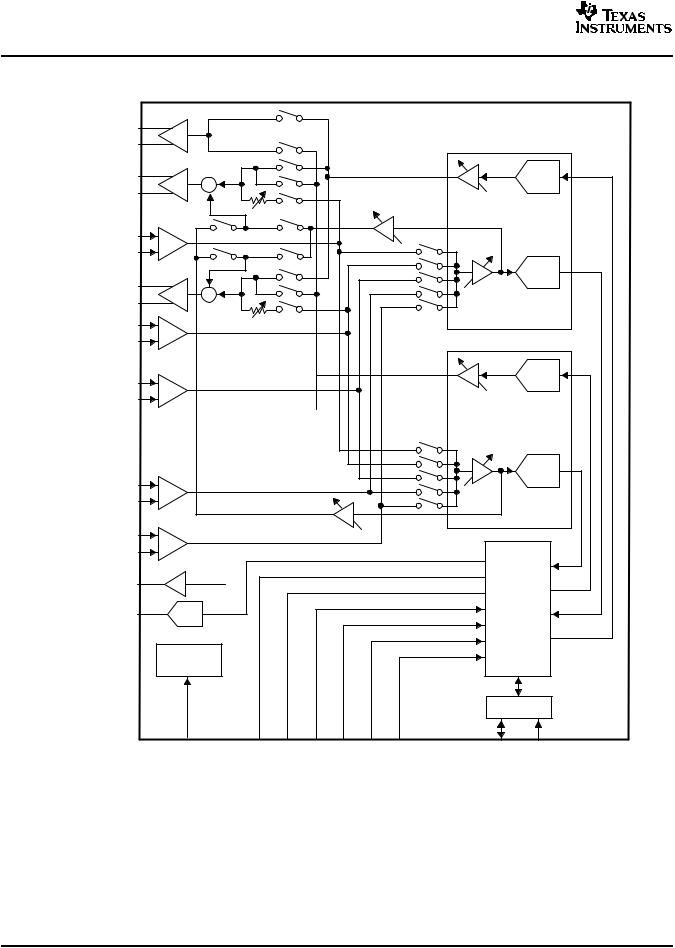
Functional Block Diagram - AIC20/21/20K
Speaker |
SPKO+ |
|
|
|
|
|
|
|
|
8 Ω Output |
SPKO- |
|
|
|
|
|
|
|
|
|
|
|
|
|
|
|
|
|
|
Line Output |
LINE0+ |
|
|
|
|
|
|
|
|
|
|
|
|
|
|
|
|
|
|
600 Ω |
LINEO- |
|
|
|
|
|
|
CODEC 1 (Channel 1) |
|
|
|
|
|
|
|
|
|||
|
HNSO+ |
|
|
|
|
|
|
|
Σ- |
Handset |
+ |
|
|
|
|
|
|
DAC |
|
|
|
|
|
|
|
|
|||
150 Ω Output |
HNSO- |
|
|
|
|
|
|
|
|
|
|
|
Analog Sidetone |
0dB to -42 dB |
|
||||
|
|
|
|
|
|||||
|
|
|
|
|
-9 dB to -27 dB |
(1.5 dB Steps). |
|
||
|
|
|
|
|
|
|
|
-48 dB, -54 dB |
|
Handset |
HNSI+ |
|
|
|
|
|
|
|
|
|
|
|
|
|
|
|
|
|
|
Input |
HNSI- |
|
|
|
|
|
|
|
|
|
|
|
|
|
|
|
|
|
|
|
|
|
|
|
|
|
|
|
Σ- |
|
|
|
|
|
|
|
|
|
ADC |
Headset |
HDSO+ |
+ |
|
|
|
|
|
|
|
|
|
|
|
|
|
0dB to 42dB |
|
||
150 Ω Output |
HDSO- |
|
|
|
|
|
|
||
|
|
|
|
|
|
|
|||
|
|
|
|
|
|
|
(1.5 dB Steps). |
|
|
|
|
|
|
|
|
|
|
48 dB, 54 dB |
|
Headset |
HDSI+ |
|
|
|
|
|
|
|
|
|
|
|
|
|
|
|
|
|
|
Input |
HDSI- |
|
|
|
|
|
|
CODEC 2 (Channel 2) |
|
|
|
|
|
|
|
|
|||
|
|
|
|
|
|
|
|
|
Σ- |
Microphone |
MICI+ |
|
|
|
|
|
|
|
DAC |
|
|
|
|
|
|
|
|
||
|
|
|
|
|
|
|
0dB to -42 dB |
|
|
Input |
MICI- |
|
|
|
|
|
|
|
|
|
|
|
|
|
|
|
(1.5 dB Steps). |
|
|
|
|
|
|
|
|
|
|
|
|
|
|
|
|
|
|
|
|
-48 dB, -54 dB |
|
|
|
|
|
|
|
|
|
0dB to 42dB |
|
|
|
|
|
|
|
|
|
(1.5 dB Steps). |
|
|
|
|
|
|
|
|
|
48 dB, 54 dB |
|
|
|
|
|
|
|
|
|
|
Σ- |
|
|
|
|
|
|
|
|
|
ADC |
Line |
LINEI+ |
|
|
|
|
|
|
|
|
|
|
|
|
|
|
|
|
|
|
Input |
LINEI- |
|
|
|
|
|
|
|
|
|
|
|
|
|
|
|
|
|
|
|
|
|
|
Analog Sidetone |
|
|
|
|
|
|
CIDI+ |
|
|
-9 dB to -27 dB |
|
|
|
|
|
|
|
|
|
|
|
|
|
|
|
|
CIDI- |
|
|
|
|
|
|
|
|
|
|
1.35 V / 2.35 |
|
|
|
|
|
|
|
|
MICBIAS |
2 mA |
|
|
|
|
|
|
|
|
|
|
|
|
|
|
|
|
|
|
|
|
|
|
|
|
|
SMARTDM |
|
|
LCDAC |
DAC |
|
|
|
|
|
Serial Port |
|
|
|
Internal Clock |
|
|
|
|
|
|
|
|
|
Generator |
|
|
|
|
|
|
|
|
|
|
|
|
|
|
|
Host Port |
|
|
|
MCLK |
FSD |
DOUT |
DIN SCLK |
FS |
M/S |
SDA |
SCL |
11
TLV320AIC20, TLV320AIC21
TLV320AIC24, TLV320AIC25
TLV320AIC20K, TLV320AIC24K
www.ti.com
SLAS363D –MARCH 2002 –REVISED APRIL 2005
Functional Block Diagram - AIC24/25/24K
Line Output |
OUTP1 |
|
|
|
|
|
|
|
|
600 Ω |
OUTM1 |
|
|
|
|
|
|
CODEC 1 (Channel 1) |
|
|
|
|
|
|
|
|
|||
|
OUTP2 |
|
|
|
|
|
|
|
Σ− |
150 Ω Output |
+ |
|
|
|
|
|
|
DAC |
|
|
|
|
|
|
|
|
|||
|
OUTM2 |
|
|
|
|
|
|
|
|
|
|
|
|
Analog Sidetone |
0 dB to −42 dB |
|
|||
|
|
|
|
|
−9 dB to −27 dB |
(1.5 dB Steps). |
|
||
|
|
|
|
|
|
|
|
−48 dB, −54 dB |
|
Input |
INP2 |
|
|
|
|
|
|
|
|
|
|
|
|
|
|
|
|
|
|
|
INM2 |
|
|
|
|
|
|
|
|
|
|
|
|
|
|
|
|
|
Σ− |
|
|
|
|
|
|
|
|
|
ADC |
150 Ω Output |
OUTP3 |
+ |
|
|
|
|
|
|
|
|
|
|
|
|
|
0 dB to 42 dB |
|
||
|
OUTM3 |
|
|
|
|
|
|
||
|
|
|
|
|
|
|
(1.5 dB Steps). |
|
|
|
|
|
|
|
|
|
|
48 dB, 54 dB |
|
Input |
INP3 |
|
|
|
|
|
|
|
|
|
|
|
|
|
|
|
|
|
|
|
INM3 |
|
|
|
|
|
|
CODEC 2 (Channel 2) |
|
|
|
|
|
|
|
|
|
|
Σ− |
Microphone |
MICI+ |
|
|
|
|
|
|
|
DAC |
|
|
|
|
|
|
|
|
||
|
|
|
|
|
|
|
0 dB to −42 dB |
|
|
Input |
MICI− |
|
|
|
|
|
|
|
|
|
|
|
|
|
|
|
(1.5 dB Steps). |
|
|
|
|
|
|
|
|
|
|
|
|
|
|
|
|
|
|
|
|
−48 dB, −54 dB |
|
|
|
|
|
|
|
|
|
0 dB to 42 dB |
|
|
|
|
|
|
|
|
|
(1.5 dB Steps). |
|
|
|
|
|
|
|
|
|
48 dB, 54 dB |
|
|
|
|
|
|
|
|
|
|
Σ− |
|
|
|
|
|
|
|
|
|
ADC |
Input |
INP1 |
|
|
|
|
|
|
|
|
|
|
|
|
|
|
|
|
|
|
|
INM1 |
|
|
|
|
|
|
|
|
|
|
|
|
Analog Sidetone |
|
|
|
|
|
Input |
INP4 |
|
|
−9 dB to −27 dB |
|
|
|
|
|
|
|
|
|
|
|
|
|
||
|
|
|
|
|
|
|
|
|
|
|
INM4 |
|
|
|
|
|
|
|
|
|
|
1.35 V / 2.35 |
|
|
|
|
|
|
|
|
MICBIAS |
2 mA |
|
|
|
|
|
|
|
|
|
|
|
|
|
|
|
|
|
|
|
|
|
|
|
|
|
SMARTDM |
|
|
LCDAC |
DAC |
|
|
|
|
|
Serial Port |
|
|
|
Internal Clock |
|
|
|
|
|
|
|
|
|
Generator |
|
|
|
|
|
|
|
|
|
|
|
|
|
|
|
Host Port |
|
|
|
MCLK |
FSD |
DOUT |
DIN SCLK |
FS |
M/S |
SDA |
SCL |
12
TLV320AIC20, TLV320AIC21
TLV320AIC24, TLV320AIC25
TLV320AIC20K, TLV320AIC24K
www.ti.com
SLAS363D –MARCH 2002 –REVISED APRIL 2005
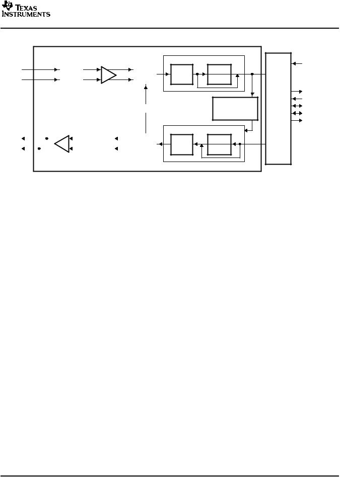
Functional Block Diagram (One of Two Channels Shown)
|
|
|
|
|
|
|
|
|
|
|
CODEC |
||||
|
|
|
|
|
|
|
|
|
|
|
|
|
|||
|
|
|
|
|
|
Anti- |
|
|
|
|
Sigma- |
||||
|
|
|
|
Aliasing |
|
PGA |
|
|
Delta |
||||||
|
|
|
|
|
|
Filter |
|
|
|
|
|
|
|
ADC |
|
|
|
|
|
|
|
|
|
|
|
|
|||||
|
|
|
|
|
|
|
|
0 dB to 42 dB (1.5 dB Steps) |
|||||||
|
|
|
|
|
|
|
|
|
48 dB, 54 dB |
|
|
|
|
|
|
|
|
|
|
|
|
Analog |
|
|
|
|
|
|
|
|
|
|
|
|
|
|
|
|
|
|
|
|
|
|
|||
|
|
|
|
|
|
Loopback |
|
|
|
|
|
|
|
|
|
|
|
|
|
|
|
|
|
|
|
|
|
|
|
Vref |
|
|
|
|
|
|
|
|
|
|
|
|
|
||||
|
|
|
|
|
|
|
|
|
|
|
|
|
|
|
|
|
|
|
|
|
|
|
|
|
|
|
|
|
Sigma- |
||
|
|
|
|
|
|
|
|
|
Low Pass |
|
|
|
|||
|
|
|
PGA |
|
Filter |
|
|
|
Delta |
||||||
|
|
|
|
|
|
|
|
|
|
|
|
|
DAC |
||
|
|
|
|
|
|
|
|
|
|
|
|
|
|
||
|
|
0 dB to -42 dB (1.5 dB Steps) |
|
|
|
|
|
||||||||
|
|
|
|
|
|
|
|||||||||
|
|
|
|
|
|
-48 dB, -54 dB |
|
|
|
|
|
||||
Decimation Filter |
|
SMARTDM |
M/S |
|
|
Serial |
|
|
FIR Filter |
|
|
Sinc |
Port |
|
|
|
|
||
Filter |
IIR Filter |
|
|
|
|
|
|
|
|
|
DOUT |
|
Digital Loopback |
|
DIN |
|
|
|
|
|
w/ Sidetone Control |
|
FS |
|
and Mute |
|
SCLK |
|
-9 dB to -27 dB |
|
|
|
|
FSD |
|
|
|
|
|
Interpolation Filter |
|
|
|
Sinc |
FIR Filter |
|
|
|
|
|
|
Filter |
IIR Filter |
|
|
|
|
|
|
Definitions and Terminology |
Data Transfer |
The time during which data is transferred from DOUT and to DIN. |
Interval |
The interval is 16 shift clocks, and the data transfer is initiated by |
|
the falling edge of the FS signal. |
Signal Data |
This refers to the input signal and all of the converted representations |
|
through the ADC channel and the signal through the DAC channel to the |
|
analog output. This is contrasted with the purely digital software control |
|
data. |
Frame Sync |
Frame sync refers only to the falling edge of the signal FS that initiates |
|
the data transfer interval |
Frame Sync and Sampling Period |
Frame sync and sampling period is the time between falling edges of |
|
successive FS signals. |
fs |
The sampling frequency |
ADC Channel |
ADC channel refers to all signal processing circuits between the analog |
|
input and the digital conversion result at DOUT. |
DAC channel |
DAC channel refers to all signal processing circuits between the digital |
|
data word applied to DIN and the differential output analog signal |
|
available at OUTP and OUTM. |
Dxx |
Bit position in the primary data word (xx is the bit number) |
DSxx |
Bit position in the secondary data word (xx is the bit number) |
d |
The alpha character d represents valid programmed or default data in the |
|
control register format (see Section 3.2, Secondary Serial Communi- |
|
cation) when discussing other data bit portions of the register. |
PGA |
Programmable gain amplifier |
IIR |
Infinite impulse response |
FIR |
Finite impulse response |
13
TLV320AIC20, TLV320AIC21 |
|
|
|
|
|
|
|
|
|
|
|
|
|
|
|
|
|
|
|
|
|
|
|
|
|
|
|
|
|
|
|
|
|
|
|
|
|
|
|
|
|
|
|
|
|
|
|
|
|
|
|
|
|
|
|
|
|
|
|
|
|
|
|||||||||||||||||||
TLV320AIC24, TLV320AIC25 |
|
|
|
|
|
|
|
|
|
|
|
|
|
|
|
|
|
|
|
|
|
|
|
|
|
|
|
|
|
|
|
|
|
|
|
|
|
|
|
|
|
|
|
|
|
|
|
|
|
|
|
|
|
|
|
|
|
|
|
|
|
|
|||||||||||||||||||
TLV320AIC20K, TLV320AIC24K |
|
|
|
|
|
|
|
|
|
|
|
|
|
|
|
|
|
|
|
|
|
|
|
|
|
|
|
|
|
|
|
|
|
|
|
|
|
|
|
|
|
|
|
|
|
|
|
|
|
|
|
|
|
|
|
|
|
|
|
|
www.ti.com |
||||||||||||||||||||
SLAS363D –MARCH 2002 –REVISED APRIL 2005 |
|
|
|
|
|
|
|
|
|
|
|
|
|
|
|
|
|
|
|
|
|
|
|
|
|
|
|
|
|
|
|
|
|
|
|
|
|
|
|
|
|
|
|
|
|
|
|
|
|
|
|
|
|
|
|
|
|
|
|
|
|||||||||||||||||||||
|
|
|
|
|
|
|
|
|
|
|
|
|
|
|
|
|
|
|
|
|
|
|
|
|
|
|
|
|
|
|
|
|
|
|
|
|
|
|
|
|
|
|
|
|
|
|
|
|
|
|
|
|
|
|
|
|
|
|
|
|
|
||||||||||||||||||||
|
|
|
|
|
|
|
|
|
|
|
|
|
|
|
|
|
|
|
|
|
|
TIMING REQUIREMENTS |
|
|
|
|
|
|
|
|
|
|
|
|
|
|
|||||||||||||||||||||||||||||||||||||||||||||
|
|
|
|
|
|
|
|
|
|
|
|
|
twH |
|
|
|
|
|
|
|
|
|
|
|
|
|
2.4 V |
|
|
|
|
|
|
|
|
|
|
|
|
|
|
|
|
|
|
|
2.4 V |
|
|
|
|
|
|
|
|
|
|
|
|
|
|
|
|
|
|
|
|
|
|||||||||||||
|
|
|
|
|
|
|
|
|
|
|
|
|
|
|
|
|
|
|
|
|
|
|
|
|
|
|
|
|
|
|
|
|
|
|
|
|
|
|
|
|
|
|
|
|
|
|
|
|
|
|
|
|
|
|
|
|
|
|
|
|
|
|
|
|
|
||||||||||||||||
|
|
|
|
|
|
|
MCLK |
|
|
|
|
twL |
|
|
|
|
|
|
|
|
|
|
|
|
|
|
|
|
|
|
|
|
|
|
|
|
|
|
|
|
|
|
|
|
|
|
|
|
|
|
|
|
|
|
|
||||||||||||||||||||||||||
|
|
|
|
|
|
|
|
|
|
|
|
|
|
|
|
|
|
|
|
|
|
|
|
|
|
|
|
|
|
|
|
|
|
|
|
|
|
|
|
|
|||||||||||||||||||||||||||||||||||||||||
|
|
|
|
|
|
|
|
|
|
|
|
|
|
|
|
|
|
|
|
|
|
|
|
|
|
|
|
|
|
|
|
|
|
|
|
|
|
|
|
|
|
|
|
|
|
|
|
|
|
|
|
|
|
|
|
|
|
|
|
|
|
|
|||||||||||||||||||
|
|
|
|
|
|
|
|
|
|
|
|
|
|
|
|
|
|
|
|
|
|
|
|
|
|
|
|
|
|
|
|
|
|
|
|
|
|
|
|
|
|
|
|
|
|
|
|
|
|
|
|
|
|
|
|
|
|
|
|
|
|
|
|
|
|
|
|
|
|
|
|
|
|
|
|
||||||
|
|
|
|
|
|
|
|
|
|
|
|
|
|
|
|
|
|
|
|
|
|
|
|
|
|
|
|
|
|
|
|
|
|
|
|
|
|
|
|
|
|
|
|
|
|
tsu1 |
|
|
|
|
|
|
|
|
|
|
|
|
|
|
|
|
|
|
|
||||||||||||||||
|
|
|
|
|
|
|
|
|
|
|
|
|
|
|
|
|
|
|
|
|
|
|
|
|
|
|
|
|
|
|
|
|
|
|
|
|
|
|
|
|
|
|
|
|
|
|
|
|
|
|
|
|
|
|
|
|
|||||||||||||||||||||||||
|
|
|
|
|
|
|
|
|
|
|
|
|
|
|
|
|
|
|
|
|
|
|
|
|
|
|
|
|
|
|
|
|
|
|
|
|
|
|
|
|
|
|
|
|
|
|
|
|
th1 |
|
|
|
|
|
|
|
|
|
|
|
|
|
|
||||||||||||||||||
|
|
|
|
|
|
|
|
|
|
|
|
|
|
|
|
|
|
|
|
|
|
|
|
|
|
|
|
|
|
|
|
|
|
|
2.4 V |
|
|
|
|
|
|
|
|
|
|
|
|
|
|
|
|
|
|
|
|
||||||||||||||||||||||||||
|
|
|
|
|
|
|
|
|
|
|
|
|
|
|
|
|
|
|
|
|
|
|
|
|
|
|
|
|
|
|
|
|
|
|
|
|
|
|
|
|
|
|
|
|
|
|
|
|
|
|
|
|
|
|
|
|
|
|
|
|
|
|
|
|
|
|
|
|
|
|
|
|
|
||||||||
|
|
|
|
|
|
|
RESET |
|
|
|
|
|
|
|
|
|
|
|
|
|
|
|
|
|
|
|
|
|
|
|
|
|
|
|
|
|
|
|
|
|
|
|
|
|
|
|
|
|
|
|
|
|
|
|
|
|
|
||||||||||||||||||||||||
|
|
|
|
|
|
|
|
|
|
|
|
|
|
|
|
|
|
|
|
|
|
|
|
|
|
|
|
|
|
|
|
|
|
|
|
|
|
|
|
|
|
|
|
|
|
|
|
|
|
|
|
|
|
|
|
|
|
|
|
|
|
|
|
|
|
|
|
|
|||||||||||||
|
|
|
|
|
|
|
|
|
|
|
|
|
|
|
|
|
|
|
|
|
|
|
|
|
|
|
|
|
|
|
|
|
|
|
|
|
|
|
|
|
|
|
|
|
|
|
|
|
|
|
|
|
|
|
|
|
|
|
|
|
|
|
|
|
|
|
|
|
|
|
|
|
|
|
|
||||||
|
|
|
|
|
|
|
|
|
|
|
|
|
|
|
|
|
|
|
|
Figure 1. Hardware Reset Timing |
|
|
|
|
|
|
|
|
|
|
|
|
|
|
|||||||||||||||||||||||||||||||||||||||||||||||
|
|
|
|
|
|
|
|
|
|
|
|
|
|
|
|
|
|
|
|
|
|
|
|
|
|
|
|
|
|
|
|
|
|
|
|
|
|
|
|
|
|
|
|
|
|
|
|
|
|
|
|
|
|
|
|
|
|
|
|
|
|
|
|
|
|
|
|
|
|
|
|
|
|
|
|
|
|
|
|
||
|
SCLK |
|
|
|
|
|
|
|
|
|
|
|
|
|
|
|
|
|
|
|
|
|
|
|
|
|
|
|
|
|
|
|
|
|
|
|
|
|
|
|
|
|
|
|
|
|
|
|
|
|
|
|
|
|
|
|
|
|
|
|
|
|
|
||||||||||||||||||
|
|
|
|
|
|
|
|
|
|
|
|
|
|
|
|
|
|
|
|
|
|
|
|
|
|
|
|
|
|
|
|
|
|
|
|
|
|
|
|
|
|
|
|
|
|
|
|
|
|
|
|
|
|
|
|
|
|
|
|
|
|
|
|
|
|
|
|
|
|
|
|
|
|
|
|
|
|
|
|||
|
|
|
|
|
|
|
td1 |
|
|
|
|
|
|
|
|
|
|
|
|
|
|
|
|
|
|
|
|
|
|
|
|
|
|
|
|
|
|
|
|
|
|
|
|
|
|
|
|
|
|
|
|
|
|
|
|
|
|
|
|
|
t |
|
|
|
|
||||||||||||||||
|
|
|
|
|
|
|
|
|
|
|
|
|
|
|
|
|
|
|
|
|
|
|
|
|
|
|
|
|
|
|
|
|
|
|
|
|
|
|
|
|
|
|
|
|
|
|
|
|
|
|
|
|
|
|
|
|
|
|
|||||||||||||||||||||||
|
|
|
|
|
|
|
|
|
|
|
|
|
|
|
|
|
|
|
|
|
|
|
|
|
|
|
|
|
|
|
|
|
|
|
|
|
|
|
|
|
|
|
|
|
|
|
|
|
|
|
|
|
|
|
|
|
|
|
|
|
|
|
|
|
|
|
|
||||||||||||||
|
|
|
|
|
|
|
|
|
|
|
|
|
|
|
|
|
|
|
|
|
|
|
|
|
|
|
|
|
|
|
|
td2 |
|
|
|
|
|
|
|
|
|
|
td1 |
|
|
|
|
|
|
|
|
|
|
|
|
|
|
|
|
|
|
|
|
|
d2 |
|
|
|
|||||||||||||
|
FS |
|
|
|
|
|
|
|
|
|
|
|
|
|
|
|
|
|
|
|
|
|
|
|
|
|
|
|
|
|
|
|
|||||||||||||||||||||||||||||||||||||||||||||||||
|
|
|
|
|
|
|
|
|
|
|
|
|
|
|
|
|
|
|
|
|
|
|
|
|
|
|
|
|
|
|
|
|
|
|
|
|
|
|
|
|
|
|
|
|
|
|
|
|
|
|
|
|
|
|
|
|
|
|
|
|
|
|
|||||||||||||||||||
|
|
|
|
|
|
|
|
|
|
|
|
|
|
|
|
|
|
|
|
|
|
|
|
|
|
|
|
|
|
|
|
|
|
|
|
|
|
|
|
|
|
|
|
|
|
|
|
|
|
|
|
|
|
|
|
|
|
|
|
|
|
|
|
|
|
|
|
|
|
|
|
|
|
||||||||
|
FSD |
|
|
|
|
|
|
|
|
|
|
|
|
|
|
|
|
|
|
|
|
|
|
|
|
|
|
|
|
|
|
|
|
|
|
|
|
|
|
|
|
|
|
|
|
|
|
|
|
|
|
|
|
|
|
|
|
|
|
|
|
|
|
||||||||||||||||||
|
|
|
|
|
|
|
|
|
|
|
|
|
|
|
|
|
|
|
|
|
|
|
|
|
|
|
|
|
|
|
|
|
|
|
|
|
|
|
|
|
|
|
|
|
|
|
|
|
|
|
|
|
|
|
|
|
|
|
|
|
|
|
|||||||||||||||||||
|
|
|
|
|
|
|
|
|
|
|
|
|
|
|
|
|
|
|
|
|
|
|
|
|
|
|
|
|
|
|
|
|
|
|
|
|
|
|
|
|
|
|
|
|
|
|
|
|
|
|
|
|
|
|
|
|
|
|
|
|
|
|
|
|
|
|
|
|
|
||||||||||||
|
|
|
|
|
|
ten |
|
|
|
|
|
|
|
|
|
|
|
|
|
td3 |
|
|
|
tdis |
|
|
|
|
|
|
|
|
|
|
|
|
|
|
|
|
|
|
|
|
|
|
|
|
|
|
|
|
|
|
|
|
|
|
|
||||||||||||||||||||||
|
|
|
|
|
|
|
|
|
|
|
|
|
|
|
|
|
|
|
|
|
|
|
|
|
|
|
|
|
|
|
|
|
|
|
|
|
|
|
|
|
|
|
|
|
|
|
|
|
|
|
|
|
|
|
|||||||||||||||||||||||||||
|
|
|
|
|
|
|
|
|
|
|
|
|
|
|
|
|
|
|
|
|
|
|
|
|
|
|
|
|
|
|
|
|
|
|
|
|
|
|
|
|
|
|
|
|
|
|
|
|
|
|
|
|
|
|
|
|
|
|
|||||||||||||||||||||||
|
DOUT |
|
|
|
|
|
|
|
|
D15 |
|
|
|
|
|
|
|
|
|
|
|
|
|
|
|
|
|
|
|
|
|
|
|
|
|
|
|
|
|
|
|
|
|
|
|
|
|
|
|
||||||||||||||||||||||||||||||||
|
|
|
|
|
|
|
|
|
|
|
|
|
|
|
|
|
|
|
|
|
|
|
|
|
|
|
|
|
|
|
|
|
|
|
|
|
|
|
|
|
|
|
|
|
|
|
|
|
|
|
|
|
|
|
|
|
|
||||||||||||||||||||||||
|
|
|
|
|
|
|
|
|
|
|
|
|
|
|
|
|
|
|
|
|
|
|
|
|
|
|
|
|
|
|
|
|
|
|
|
|
|
|
|
|
|
|
|
|
|
|
|
|
|
|
|
|
|
|
|
|
|
|
|
|
|
|
|
|
|
|
|
|
|
|
|
|
|
|
|
||||||
|
|
|
|
|
|
|
|
|
|
|
th2 |
|
|
|
|
|
|
|
|
|
|
|
|
|
|
|
|
tsu2 |
|
|
|
|
|
|
|
|
|
|
|
|
|
|
|
|
|
|
|
|
|
|
|
|
|
|
|
|
|
|
|
|
|
|
|
|
|
|
|
||||||||||||||
|
|
|
|
|
|
|
|
|
|
|
|
|
|
|
|
|
|
|
|
|
|
|
|
|
|
|
|
|
|
|
|
|
|
|
|
|
|
|
|
|
|
|
|
|
|
|
|
|
|
|
|
|
|
|
|
|
|
|
|
|
|
|
|
|
|
||||||||||||||||
|
|
|
|
|
|
|
|
|
|
|
|
|
|
|
|
|
|
|
|
|
|
|
|
|
|
|
|
|
|
|
|
|
|
|
|
|
|
|
|
|
|
|
|
|
|
|
|
|
|
|
|
|
|
|
|
|
|
|
|
|
|
|
|
|
|
|
|
|
|
|
|
|
|
||||||||
|
DIN |
|
|
|
D15 |
|
|
|
|
|
|
|
|
|
|
|
|
|
|
|
|
|
|
|
|
|
|
|
|
|
|
|
|
|
|
|
|
|
|
|
|
|
|
|
|
|
|
|
|||||||||||||||||||||||||||||||||
|
|
|
|
|
|
|
|
|
|
|
|
|
|
|
|
|
|
|
|
|
|
|
|
|
|
|
|
|
|
|
|
|
|
|
|
|
|
|
|
|
|
|
|
|
|
|
|
|
|||||||||||||||||||||||||||||||||
|
|
|
|
|
|
|
|
|
|
|
|
|
|
|
|
|
Figure 2. Serial Communication Timing |
|
|
|
|
|
|
|
|
|
|
|
|
|
|
||||||||||||||||||||||||||||||||||||||||||||||||||
|
|
|
|
|
|
|
|
|
|
|
|
|
|
|
|
|
|
|
|
|
|
|
|
|
|
|
|
|
|
|
|
|
|
|
|
|
|
|
|
|
|
|
|
|
|
|
|
TEST CONDITIONS |
|
MIN TYP MAX |
UNIT |
||||||||||||||||||||||||||||||
twH |
Pulse duration, MCLK high |
|
|
|
|
|
|
|
|
|
|
|
|
|
|
|
|
|
|
|
|
|
|
|
|
|
|
|
|
|
|
|
|
|
|
|
|
|
|
|
|
|
|
|
|
|
|
|
|
5 |
|
|
|
|
|
|
|
|
|
|
|||||||||||||||||||||
twL |
Pulse duration, MCLK low |
|
|
|
|
|
|
|
|
|
|
|
|
|
|
|
|
|
|
|
|
|
|
|
|
|
|
|
|
|
|
|
|
|
|
|
|
|
|
|
|
|
|
|
|
|
|
|
|
5 |
|
|
|
|
|
|
|
|
|
|
|||||||||||||||||||||
tsu1 |
Setup time, RESET, before MCLK high (see Figure 1) |
|
|
|
|
|
|
|
|
|
|
|
|
|
|
|
|
|
|
|
|
|
|
|
|
|
3 |
|
|
|
|
|
|
|
|
|
|
||||||||||||||||||||||||||||||||||||||||||||
th1 |
Hold time, RESET, after MCLK high (see Figure 1) |
|
|
|
|
|
|
|
|
|
|
|
|
|
|
|
|
|
|
|
|
|
|
|
|
|
2 |
|
|
|
|
|
|
|
|
|
|
||||||||||||||||||||||||||||||||||||||||||||
td1 |
Delay time, SCLK− to FS/FSD↓ |
|
|
|
|
|
|
|
|
|
|
|
|
|
|
|
|
|
|
|
|
|
|
|
|
|
|
|
|
CL = 20 pF |
5 |
ns |
|||||||||||||||||||||||||||||||||||||||||||||||||
td2 |
Delay time, SCLK− to FS/FSD− |
|
|
|
|
|
|
|
|
|
|
|
|
|
|
|
|
|
|
|
|
|
|
|
|
|
|
|
|
|
|
|
|
|
|
|
|
|
|
|
|
|
|
|
|
|
|
|
|
5 |
|
||||||||||||||||||||||||||||||
td3 |
Delay time, SCLK− to DOUT |
|
|
|
|
|
|
|
|
|
|
|
|
|
|
|
|
|
|
|
|
|
|
|
|
|
|
|
|
|
|
|
|
|
|
|
|
|
|
|
|
|
|
|
|
|
|
|
|
15 |
|
||||||||||||||||||||||||||||||
ten |
Enable time, SCLK− to DOUT |
|
|
|
|
|
|
|
|
|
|
|
|
|
|
|
|
|
|
|
|
|
|
|
|
|
|
|
|
|
|
|
|
|
|
|
|
|
|
|
|
|
|
|
|
|
|
|
|
15 |
|
||||||||||||||||||||||||||||||
tdis |
Disable time, SCLK− to DOUT |
|
|
|
|
|
|
|
|
|
|
|
|
|
|
|
|
|
|
|
|
|
|
|
|
|
|
|
|
|
|
|
|
|
|
|
|
|
|
|
|
|
|
|
|
|
|
|
|
15 |
|
||||||||||||||||||||||||||||||
tsu2 |
Setup time, DIN, before SCLK↓ |
|
|
|
|
|
|
|
|
|
|
|
|
|
|
|
|
|
|
|
|
|
|
|
|
|
|
|
|
|
|
|
|
|
|
|
|
|
|
|
|
|
|
|
|
|
|
|
|
10 |
|
|
|
|
|
|
|
|
|
|
|||||||||||||||||||||
th2 |
Hold time, DIN, after SCLK↓ |
|
|
|
|
|
|
|
|
|
|
|
|
|
|
|
|
|
|
|
|
|
|
|
|
|
|
|
|
|
|
|
|
|
|
|
|
|
|
|
|
|
|
|
|
|
|
|
|
10 |
|
|
|
|
|
|
|
|
|
|
|||||||||||||||||||||
14
TLV320AIC20, TLV320AIC21
TLV320AIC24, TLV320AIC25
TLV320AIC20K, TLV320AIC24K
www.ti.com
SLAS363D –MARCH 2002 –REVISED APRIL 2005
SDA |
|
|
|
|
|
|
|
|
|
|
|
|
|
|
|
|
|
|
|
|
|
|
|
|
|
|
|
|
|
|
|
|
|
|
|
|
|
|
|
|
|
|
|
|
|
|
|
|
|
|
|||||||||
|
|
|
|
|
|
|
|
|
|
|
|
|
|
|
|
|
|
|
|
|
|
|
|
|
|
|
|
|
|
|
|
|
|
|
|
|
|
|
|
|
|
|
|
|
|
|
|
|
|
|
|
|
|
|
|
|
|
|
|
tf |
|
|
|
|
|
|
|
|
|
|
|
|
|
|
|
|
|
|
|
|
|
|
|
tSU;DAT |
|
|
|
|
|
|
|
|
|
|
|
|
|
|
|
|
|
|
|
|
|
|
|||||||||||||
|
|
|
tLOW |
|
tr |
|
|
|
|
|
|
|
|
|
|
tHD;STA |
|
|
|
tr |
|
|
|
|
|
|
tBUF |
||||||||||||||||||||||||||||||||
|
|
|
|
|
|
|
|
|
|
|
|
|
|
|
|
|
|
|
tf |
|
|
|
|
|
|
|
|
|
|
|
|
|
|
|
|
||||||||||||||||||||||||
|
|
|
|
|
|
|
|
|
|
|
|
|
|
|
|
|
|
|
|
|
|
|
|
|
|
|
|
|
|
|
|
|
|
|
|
|
|
|
|
|
|
|
|
|
|
|
|||||||||||||
SCL |
|
|
|
|
|
|
|
|
|
|
|
|
|
|
|
|
|
|
|
|
|
|
|
|
|
|
|
|
|
|
|
|
|
|
|
|
|
|
|
|
|
|
|
|
|
|
|
|
|
|
|||||||||
|
|
|
|
|
|
|
|
|
|
|
|
|
|
|
|
|
|
|
|
|
|
|
|
|
|
|
|
|
|
|
|
|
|
|
|
|
|
|
|
|
|
|
|
|
|
|
|
|
|
|
|
|
|
|
|
|
|
||
|
|
|
|
|
|
|
|
tHD;STA |
|
|
|
|
|
|
|
|
|
|
|
|
|
|
|
|
|
|
|
t |
|
|
|
|
|
|
|
|
|
|
|
|
|
|
|
|
|
|
|
|
|
|
|||||||||
|
|
|
|
|
|
|
|
|
|
|
|
|
|
|
|
|
|
|
|
|
|
|
|
|
|
|
|
|
|
|
|
|
|
|
|
|
|
|
|
|
|
|
|
|
|
|
|
|
|||||||||||
|
|
|
|
|
|
|
|
tHD;DAT |
|
|
|
|
|
|
|
|
|
|
|
|
|
|
|
|
|
|
|
HIGH |
|
|
|
|
|
|
|
|
|
tSU;STO |
|
|
|
|
|
|
|
|
|
|
|||||||||||
|
|
|
|
|
|
|
|
|
|
|
|
|
|
|
|
|
|
|
|
|
|
|
|
|
|
|
|
tSU;STA |
|
|
|
|
|
|
|
|
|
|
|
|
|
|
|
|
|
|
|
|
|
|
|
||||||||
|
|
|
|
|
|
|
|
|
|
|
|
|
|
|
|
|
|
|
|
|
|
|
|
|
|
|
|
|
|
|
|
|
|
|
|
|
|
|
|
|
|
|
|
|
|||||||||||||||
|
|
|
|
|
|
|
|
|
|
|
|
|
|
|
|
|
|
|
|
|
Figure 3. I2C / S2C Timing Diagram |
|
|
|
|
|
|
|
|
|
|
|
|
|
|
||||||||||||||||||||||||
|
|
|
|
|
|
|
|
|
|
PARAMETER |
|
|
|
|
|
|
|
|
|
|
|
|
|
|
|
|
|
|
|
SYMBOL |
|
|
MIN |
|
|
MAX |
UNIT |
||||||||||||||||||||||
SCL clock frequency |
|
|
|
|
|
|
|
|
|
|
|
|
|
|
|
|
|
|
|
|
|
|
|
|
|
|
|
|
|
|
|
|
tSCL |
0 |
|
|
|
|
900 |
kHz |
|||||||||||||||||||
Hold time (repeated START condition. After this period, the first clock pulse is |
|
|
|
tHD;STA |
100 |
|
|
|
|
|
|
|
|
|
|
||||||||||||||||||||||||||||||||||||||||||||
generated. |
|
|
|
|
|
|
|
|
|
|
|
|
|
|
|
|
|
|
|
|
|
|
|
|
|
|
|
|
|
|
|
|
|
|
|
|
|
|
|
|
|
|
|
|
|
|
|
|
|
|
|||||||||
Low period of the SCL clock |
|
|
|
|
|
|
|
|
|
|
|
|
|
|
|
|
|
|
|
|
|
|
|
|
|
|
|
|
|
|
|
tLOW |
560 |
|
|
|
|
|
|
|
|
|
|
||||||||||||||||
High period of the SCL clock |
|
|
|
|
|
|
|
|
|
|
|
|
|
|
|
|
|
|
|
|
|
|
|
|
|
|
|
|
|
|
|
tHIGH |
560 |
|
|
|
|
|
|
|
|
|
|
||||||||||||||||
Set-up time for a repeated START condition |
|
|
|
|
|
|
|
|
|
|
|
|
|
|
|
|
|
|
|
|
tSU;STA |
100 |
|
|
|
|
|
|
|
|
|
|
|||||||||||||||||||||||||||
Data hold time |
|
|
|
|
|
|
|
|
|
|
|
|
|
|
|
|
|
|
|
|
|
|
|
|
|
|
|
|
|
|
|
tHD;DAT |
50 |
|
|
|
|
|
|
|
ns |
||||||||||||||||||
Data set-up time |
|
|
|
|
|
|
|
|
|
|
|
|
|
|
|
|
|
|
|
|
|
|
|
|
|
|
|
|
|
|
|
tSU;DAT |
50 |
|
|
|
|
|
|
|
|
|
|
||||||||||||||||
Rise time of both SDA and SCL signals |
|
|
|
|
|
|
|
|
|
|
|
|
|
|
|
|
|
|
|
|
|
|
tr |
|
|
|
|
|
|
|
|
300 |
|
|
|
||||||||||||||||||||||||
Fall time of both SDA and SCL signals |
|
|
|
|
|
|
|
|
|
|
|
|
|
|
|
|
|
|
|
|
|
|
tf |
|
|
|
|
|
|
|
|
100 |
|
|
|
||||||||||||||||||||||||
Set-up time for STOP condition |
|
|
|
|
|
|
|
|
|
|
|
|
|
|
|
|
|
|
|
|
|
|
|
|
|
|
|
|
|
|
|
tSU;STO |
100 |
|
|
|
|
|
|
|
|
|
|
||||||||||||||||
Bus free time between a STOP and START condition |
|
|
|
|
tBUF |
500 |
|
|
|
|
|
|
|
|
|
|
|||||||||||||||||||||||||||||||||||||||||||
15
TLV320AIC20, TLV320AIC21
TLV320AIC24, TLV320AIC25
TLV320AIC20K, TLV320AIC24K
www.ti.com
SLAS363D –MARCH 2002 –REVISED APRIL 2005
PARAMETER MEASUREMENT INFORMATION
|
0 |
|
|
|
|
|
|
|
|
|
−20 |
|
|
|
|
|
|
|
|
dB |
−40 |
|
|
|
|
|
|
|
|
− |
|
|
|
|
|
|
|
|
|
Amplitude |
−60 |
|
|
|
|
|
|
|
|
−80 |
|
|
|
|
|
|
|
|
|
−100 |
|
|
|
|
|
|
|
|
|
|
|
|
|
|
|
|
|
|
|
|
−120 |
|
|
|
|
|
|
|
|
|
−140 |
500 |
1000 |
1500 |
2000 |
2500 |
3000 |
3500 |
4000 |
|
0 |
||||||||
|
|
|
|
|
f − Frequency − Hz |
|
|
|
|
|
|
|
Figure 4. |
FFT—ADC Channel (-3 dB input) |
|
|
|||
|
0 |
|
|
|
|
|
|
|
|
|
−20 |
|
|
|
|
|
|
|
|
dB |
−40 |
|
|
|
|
|
|
|
|
− |
|
|
|
|
|
|
|
|
|
Amplitude |
−60 |
|
|
|
|
|
|
|
|
−80 |
|
|
|
|
|
|
|
|
|
−100 |
|
|
|
|
|
|
|
|
|
|
|
|
|
|
|
|
|
|
|
|
−120 |
|
|
|
|
|
|
|
|
|
−140 |
500 |
1000 |
1500 |
2000 |
2500 |
3000 |
3500 |
4000 |
|
0 |
||||||||
|
|
|
|
|
f − Frequency − Hz |
|
|
|
|
|
|
|
Figure 5. FFT—ADC Channel (-9 dB input) |
|
|
|
|||||
|
0 |
|
|
|
|
|
|
|
|
|
|
|
−20 |
|
|
|
|
|
|
|
|
|
|
dB |
−40 |
|
|
|
|
|
|
|
|
|
|
− |
|
|
|
|
|
|
|
|
|
|
|
Amplitude |
−60 |
|
|
|
|
|
|
|
|
|
|
−80 |
|
|
|
|
|
|
|
|
|
|
|
−100 |
|
|
|
|
|
|
|
|
|
|
|
|
|
|
|
|
|
|
|
|
|
|
|
|
−120 |
|
|
|
|
|
|
|
|
|
|
|
−140 |
2000 |
4000 |
6000 |
8000 |
10000 |
12000 |
14000 |
16000 |
18000 |
20000 |
|
0 |
||||||||||
|
|
|
|
|
f − Frequency − Hz |
|
|
|
|
||
Figure 6. FFT—DAC Channel (0 dB input)
16

TLV320AIC20, TLV320AIC21
TLV320AIC24, TLV320AIC25
TLV320AIC20K, TLV320AIC24K
www.ti.com
SLAS363D –MARCH 2002 –REVISED APRIL 2005
PARAMETER MEASUREMENT INFORMATION (continued)
|
0 |
|
|
|
|
|
|
|
|
|
|
|
−20 |
|
|
|
|
|
|
|
|
|
|
dB |
−40 |
|
|
|
|
|
|
|
|
|
|
− |
|
|
|
|
|
|
|
|
|
|
|
Amplitude |
−60 |
|
|
|
|
|
|
|
|
|
|
−80 |
|
|
|
|
|
|
|
|
|
|
|
−100 |
|
|
|
|
|
|
|
|
|
|
|
|
|
|
|
|
|
|
|
|
|
|
|
|
−120 |
|
|
|
|
|
|
|
|
|
|
|
−140 |
2000 |
4000 |
6000 |
8000 |
10000 |
12000 |
14000 |
16000 |
18000 |
20000 |
|
0 |
||||||||||
|
|
|
|
|
f − Frequency − Hz |
|
|
|
|
||
|
|
|
Figure 7. |
FFT—DAC Channel (-9 dB input) |
|
|
|||
|
0 |
|
|
|
|
|
|
|
|
|
−20 |
|
|
|
|
|
|
|
|
dB |
−40 |
|
|
|
|
|
|
|
|
− |
|
|
|
|
|
|
|
|
|
Amplitude |
−60 |
|
|
|
|
|
|
|
|
−80 |
|
|
|
|
|
|
|
|
|
−100 |
|
|
|
|
|
|
|
|
|
|
|
|
|
|
|
|
|
|
|
|
−120 |
|
|
|
|
|
|
|
|
|
−140 |
|
|
|
|
|
|
|
|
|
0 |
2000 |
4000 |
6000 |
8000 |
10000 |
12000 |
14000 |
16000 |
|
|
|
|
|
f − Frequency − Hz |
|
|
|
|
Figure 8. FFT—ADC Channel in FIR/IIR Bypass Mode (-3 dB input)
|
0 |
|
|
|
|
|
|
|
|
|
|
|
−20 |
|
|
|
|
|
|
|
|
|
|
dB |
−40 |
|
|
|
|
|
|
|
|
|
|
− |
|
|
|
|
|
|
|
|
|
|
|
Amplitude |
−60 |
|
|
|
|
|
|
|
|
|
|
−80 |
|
|
|
|
|
|
|
|
|
|
|
−100 |
|
|
|
|
|
|
|
|
|
|
|
|
|
|
|
|
|
|
|
|
|
|
|
|
−120 |
|
|
|
|
|
|
|
|
|
|
|
−140 |
2000 |
4000 |
6000 |
8000 |
10000 |
12000 |
14000 |
16000 |
18000 |
20000 |
|
0 |
||||||||||
|
|
|
|
|
f − Frequency − Hz |
|
|
|
|
||
Figure 9. FFT—DAC Channel in FIR/IIR Bypass Mode (0 dB input)
17
Loading...