


Texas Instruments TLV1562IDW, TLV1562IDWR, TLV1562EVM, TLV1562CPWR, TLV1562CDWR Datasheet
...TLV1562 2.7 V TO 5.5 V, HIGH-SPEED LOW-POWER RECONFIGURABLE ANALOG-TO-DIGITAL CONVERTER WITH 4-INPUT, DUAL S/H, PARALLEL INTERFACE, AND POWER DOWN
SLAS162 ± SEPTEMBER 1998
D2 MSPS Max Throughput at 10 Bit (Single Channel), ±1 LSB DNL, ±1 LSB INL MAX
D3 MSPS Max Throughput at 8 Bit (Single Channel), ±1 LSB DNL, ±1 LSB INL MAX
D7 MSPS Max Throughput at 4 Bit (Single Channel), ±0.4 LSB DNL, ±0.4 LSB INL MAX
DNo Missing Code for External Clock Up to 15 MHz at 5.5 V, 12 MHz at 2.7 V
DENOB 9.4 Bit, SINAD 57.8 dB, SFDR ±70.8 dB, THD ±68.8 dB, at fi = 800 kHz, 10 Bit
DWide Input Bandwidth for Undersampling
(75 MHz at 1 dB, >120 MHz at ±3 dB) at Rs = 1 kΩ
DSoftware Programmable Power Down, (1 µA), Auto Powerdown (120 µA)
DSingle Wide Range Supply 2.7 VDC to 5.5 VDC
DLow Supply Current 11 mA at 5.5 V, 10 MHz; 7 mA at 2.7 V, 8 MHz Operating
DSimultaneous Sample and Hold:
Dual Sample and Hold Matched Channels Multi Chip Simultaneous Sample and Hold Capable
DProgrammable Conversion Modes: Interrupt-Driven for Shorter Latency Continuous Modes Optimized for MIPS Sensitive DSP Solutions
DBuilt-In Internal/System Mid-Scale Error Calibration
DBuilt-In Mux With 2 Differential or 4 Single-Ended Input Channels
DLow Input Capacitance (10 pF Max Fixed, 1 pF Max Switching)
DDSP/µ P-Compatible Parallel Interface
applications
DPortable Digital Radios
DPersonal Communication Assistants
DCellular
DPager
DScanner
DDigitizers
DProcess Controls
DMotor Control
DRemote Sensing
DAutomotive
DServo Controls
DCameras
DW OR PW PACKAGE
(TOP VIEW)
|
|
|
|
|
|
|
|
|
|
|
|
|
|
CSTART |
|
1 |
28 |
|
|
RD |
|||||||
|
|
|
|||||||||||
(LSB) D0 |
|
2 |
27 |
|
|
AP/CH1 |
|||||||
|
|
|
|||||||||||
|
|
D1 |
|
3 |
26 |
|
|
AM/CH2 |
|||||
|
|
|
|
|
|||||||||
|
|
D2 |
|
4 |
25 |
|
|
BP/CH3 |
|||||
|
|
|
|
|
|||||||||
|
|
D3 |
|
5 |
24 |
|
|
BM/CH4 |
|||||
|
|
|
|
|
|||||||||
|
|
D4 |
|
6 |
23 |
|
|
AVDD |
|||||
|
|
|
|
|
|||||||||
|
BDVDD |
|
7 |
22 |
|
|
VREFP |
||||||
|
|
|
|
||||||||||
|
BDGND |
|
8 |
21 |
|
|
VREFM |
||||||
|
|
|
|
||||||||||
|
|
D5 |
|
9 |
20 |
|
|
AGND |
|||||
|
|
|
|
|
|||||||||
|
|
D6 |
|
10 |
19 |
|
|
WR |
|
|
|||
|
|
|
|
|
|
|
|||||||
|
|
D7 |
|
11 |
18 |
|
|
DGND |
|||||
|
|
|
|
|
|||||||||
|
|
D8 |
|
12 |
17 |
|
|
DVDD |
|||||
|
|
|
|
|
|||||||||
(MSB) D9 |
|
|
|
|
|
||||||||
|
13 |
16 |
|
|
CLKIN |
||||||||
|
|
|
|
|
|
|
|
|
|
|
|
|
|
|
|
INT |
14 |
15 |
CS/OE |
||||||||
|
|
|
|
|
|
||||||||
|
|
|
|
|
|
|
|
|
|
|
|
|
|
Please be aware that an important notice concerning availability, standard warranty, and use in critical applications of Texas Instruments semiconductor products and disclaimers thereto appears at the end of this data sheet.
PRODUCTION DATA information is current as of publication date. Products conform to specifications per the terms of Texas Instruments standard warranty. Production processing does not necessarily include testing of all parameters.
Copyright 1998, Texas Instruments Incorporated
POST OFFICE BOX 655303 •DALLAS, TEXAS 75265 |
1 |
TLV1562
2.7 V TO 5.5 V, HIGH-SPEED LOW-POWER RECONFIGURABLE ANALOG-TO-DIGITAL CONVERTER WITH 4-INPUT, DUAL S/H, PARALLEL INTERFACE, AND POWER DOWN
SLAS162 ± SEPTEMBER 1998
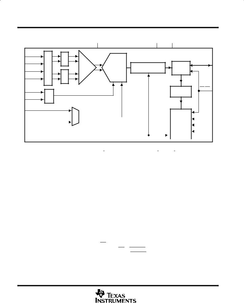
functional block diagram
AVDD |
DVDD BDVDD |
AP/CH1 |
|
|
|
|
|
|
AM/CH2 |
|
S/H |
|
|
|
D (0±9) |
M |
|
4/8/10-Bit |
|
|
||
|
|
Serial/Parallel Conv |
3-State |
|||
|
Amplifier |
|
||||
BP/CH3 |
U |
Recyclic |
|
|||
and FIFO |
Buffer |
|
||||
X |
|
ADC |
|
|||
|
|
|
|
|
||
BM/CH4 |
|
S/H |
|
|
|
|
VREFP |
|
VREFMID |
|
|
Control |
CS/OE |
|
REF |
|
|
Register |
|
|
VREFM |
|
|
|
|
|
|
|
|
|
|
|
|
CLKIN
|
(15 MHz Max) |
|
|
SysClk |
|
|
|
|
|
|
|
|
|
|
|
|
|
|
|
|
|
|
|||||||
|
|
|
|
|
|
|
|
|
|
|
|
Interface |
|
|
|
INT |
|||||||||||||
|
|
|
OSC |
|
|
|
|
|
|
|
|
|
|
|
|
|
|
|
|
|
|
|
|
|
|||||
|
|
|
|
|
|
|
|
|
|
|
|
|
|
|
|
|
|
|
|
|
|
|
|
|
|
||||
|
|
|
|
|
|
|
|
|
|
|
|
|
|
|
|
|
|
|
|
|
|
Timing |
|
|
|
|
|
||
|
|
|
|
|
|
|
|
|
|
|
|
|
|
|
|
|
|
|
|
|
|
|
|
CSTART |
|||||
|
|
|
(7.5 MHz Min) |
|
|
|
|
|
|
|
|
|
|
|
|
|
|
|
|
|
|
|
|
|
|||||
|
|
|
|
|
|
|
|
|
|
|
|
|
|
|
|
|
|
|
|
|
|
|
and |
|
|
||||
|
|
|
|
|
|
|
|
|
|
|
|
|
|
|
|
|
|
|
|
|
|
|
|
|
|
|
|
||
|
|
|
|
|
|
|
|
|
|
|
|
|
|
|
|
|
|
|
|
|
|
|
|
|
|
|
|
|
|
|
|
|
|
|
|
|
|
|
|
|
|
|
|
|
|
|
|
|
|
|
|
Control |
|
|
|
WR |
|
||
|
RD |
|
|
|
|
|
|
|
|
|
|
|
|
|
|
|
|
|
|
|
|
|
|
|
|
|
|
|
|
|
|
|
|
|
|
|
|
|
|
|
|
|
|
|
|
|
|
|
|
|
|
|
|
|
|
||||
|
|
|
|
|
|
|
|
|
|
|
|
|
|
|
|
|
|
|
|
|
|
|
|
|
|
|
|
|
|
|
|
|
|
|
|
|
|
|
|
|
AGND |
|
|
|
|
|
DGND |
|
|
|
|
|
BDGND |
|
|
|
|
|
|
|
|
|
|
|
|
|
|
|
|
|
|
|
|
|
|
|
|
|
|
|
|
|
|
|
|
||||
|
|
|
|
|
|
|
|
|
|
|
|
|
|
|
|
|
|
|
|
|
|
|
|
|
|
|
|
|
|
|
|
|
|
|
|
|
|
|
|
|
|
|
|
|
|
|
|
|
|
|
|
|
|
|
|
|
|
|
|
description
The TLV1562 is a 10-bit CMOS low-power, high-speed programmable resolution analog-to-digital converter based on a low-power recyclic architecture. The unique architecture delivers a throughput up to 2 MSPS (million samples per second) at 10-bit resolution. The programmable resolution allows a higher conversion throughput as a tradeoff of lower resolution. A high speed 3-state parallel port directly interfaces to a digital signal processor (DSP) or microprocessor ( P) system data bus. D0 through D9 are the digital output terminals with D0 being the least significant bit (LSB). The TLV1562 is designed to operate for a wide range of supply voltages (2.7 V to 5.5 V) with very low power consumption (11 mA maximum at 5.5 V, 10 MHz CLKIN). The power saving feature is further enhanced with a software power-down feature (1 A maximum) and auto power-down (1 A maximum) feature.
Many programmable features make this device a flexible general-purpose data converter. The device can be configured as either four single-ended inputs to maximize the capacity or two differential inputs to improve noise immunity. The internal system clock (SYSCLK) may come from either an internally generated OSC or an external clock source (CLKIN). Four different modes of conversion are available for different applications. The interrupt driven modes are mostly suitable for asynchronous applications, while the continuous modes take advantage of the high speed nature of a pipelined architecture. A pair of built-in sample-and-hold amplifiers allow simultaneous sampling of two input channels. This makes the TLV1562 perfect for communication applications. Conversion is started by the RD signal, which can also be used for reading data, to maximize the throughput. Conversion can be started either by the RD or CSTART signal when the device is operating in the interrupt-driven modes. The dedicated conversion start pin, CSTART, provides a mechanism to simultaneously sample and convert multiple channels when multiple converters are used in an application.
2 |
POST OFFICE BOX 655303 •DALLAS, TEXAS 75265 |

TLV1562 2.7 V TO 5.5 V, HIGH-SPEED LOW-POWER RECONFIGURABLE ANALOG-TO-DIGITAL CONVERTER WITH 4-INPUT, DUAL S/H, PARALLEL INTERFACE, AND POWER DOWN
SLAS162 ± SEPTEMBER 1998
description (continued)
The converter incorporates a pair of differential high-impedance reference inputs that facilitate ratiometric conversion, scaling, and isolation of analog circuitry from logic and supply noise. Other features such as low input capacitance (10 pF) and very wide input bandwidth (75 MHz) make this device a perfect digital signal processing (DSP) companion for mobile communication applications. A switched-capacitor design allows low-error conversion over the full operating free-air temperature range.
The features that make this device truly a DSP friendly converter include: 1) programmable continuous conversion modes, 2) programmable 2s complement output code format, and 3) programmable resolution. The TLV1562 is offered in both 28-pin TSSOP and SOIC packages. The TLV1562C is characterized for operation from 0°C to 70°C. The TLV1562I is characterized for operation over the full industrial temperature range of ±40°C to 85°C.
AVAILABLE OPTIONS
|
PACKAGED DEVICE |
||
|
|
|
|
TA |
28-TSSOP |
28-SOIC |
|
(25 MIL PITCH) |
(50 MIL PITCH) |
||
|
|||
|
(PW) |
(DW) |
|
|
|
|
|
0°C to 70°C |
TLV1562CPW |
TLV1562CDW |
|
|
|
|
|
±40°C to 85°C |
TLV1562IPW |
TLV1562IDW |
|
POST OFFICE BOX 655303 •DALLAS, TEXAS 75265 |
3 |

TLV1562
2.7 V TO 5.5 V, HIGH-SPEED LOW-POWER RECONFIGURABLE ANALOG-TO-DIGITAL CONVERTER WITH 4-INPUT, DUAL S/H, PARALLEL INTERFACE, AND POWER DOWN
SLAS162 ± SEPTEMBER 1998
|
|
|
|
|
|
|
|
|
Terminal Functions |
||||||||||||||
|
|
|
|
|
|
|
|
|
|
|
|
|
|
|
|
|
|
|
|
|
|
|
|
|
TERMINAL |
I/O |
|
|
DESCRIPTION |
||||||||||||||||||
|
NAME |
NO. |
|
|
|||||||||||||||||||
|
|
|
|
|
|
|
|
|
|
|
|
|
|
|
|
|
|||||||
|
|
|
|
|
|
|
|
|
|
|
|
|
|
|
|
|
|
|
|
|
|
|
|
|
AGND |
20 |
I |
Analog ground return for the internal circuitry. Unless otherwise noted, all analog voltage measurements are with |
|||||||||||||||||||
|
|
|
|
|
|
|
|
|
respect to AGND. |
||||||||||||||
|
|
|
|
|
|
|
|
|
|
|
|
|
|
|
|
|
|
|
|
|
|
|
|
|
AM/CH2 |
26 |
I |
Differential channel A input minus or single-ended channel 2 |
|||||||||||||||||||
|
|
|
|
|
|
|
|
|
|
|
|
|
|
|
|
|
|
|
|
|
|
|
|
|
AP/CH1 |
27 |
I |
Differential channel A input plus or single-ended channel 1 |
|||||||||||||||||||
|
|
|
|
|
|
|
|
|
|
|
|
|
|
|
|
|
|
|
|
|
|
|
|
|
AVDD |
23 |
I |
Positive analog supply voltage |
|||||||||||||||||||
|
BDGND |
8 |
I |
Digital ground return for the I/O buffers. Unless otherwise noted, all digital interface voltage measurements are with |
|||||||||||||||||||
|
|
|
|
|
|
|
|
|
respect to DGND. |
||||||||||||||
|
|
|
|
|
|
|
|
|
|
|
|
|
|
|
|
|
|
|
|
|
|
|
|
|
BDVDD |
7 |
I |
Positive digital supply voltage for I/O buffers |
|||||||||||||||||||
|
BM/CH4 |
24 |
I |
Differential channel B input minus or single-ended channel 4 |
|||||||||||||||||||
|
|
|
|
|
|
|
|
|
|
|
|
|
|
|
|
|
|
|
|
|
|
|
|
|
BP/CH3 |
25 |
I |
Differential channel B input plus or single-ended channel 3 |
|||||||||||||||||||
|
|
|
|
|
|
|
|
|
|
|
|
|
|
|
|
|
|
|
|
|
|
|
|
|
CLKIN |
16 |
I |
External clock input. (1 MHz to 15 MHz) |
|||||||||||||||||||
|
|
|
|
|
|
|
|
|
|
|
|
|
|
|
|
|
|
|
|
|
|
|
|
|
|
|
|
|
|
|
15 |
I |
Chip select. A high-to-low transition on this input resets the internal counters and controls and enables the output data |
||||||||||||||
|
CS/OE |
||||||||||||||||||||||
|
|
|
|
|
|
|
|
|
bus D(0±9) and control inputs (RD, WR) within a maximum setup time. A low-to-high transition disables the output |
||||||||||||||
|
|
|
|
|
|
|
|
|
data bus D(9±0) and WR within a maximum setup time. This signal also serves as an output enable signal when the |
||||||||||||||
|
|
|
|
|
|
|
|
|
device is programmed into both mono and dual interrupt-driven modes using CSTART as the start of conversion |
||||||||||||||
|
|
|
|
|
|
|
|
|
signal. |
||||||||||||||
|
|
|
|
|
|
|
|
|
|
|
|
|
|
|
|
|
|
|
|
|
|||
|
|
|
|
|
|
|
1 |
I |
Conversion start signal. A falling edge starts the sampling period and a rising edge starts the conversion. This signal |
||||||||||||||
|
CSTART |
|
|||||||||||||||||||||
|
|
|
|
|
|
|
|
|
acts without CS activated. CSTART connects to DVDD via a 10-kΩ pull-up resistor if not used. |
||||||||||||||
|
|
|
|
|
|
|
|
|
|
|
|
|
|
|
|
|
|
|
|||||
|
D(0±4) |
2±6 |
I/O |
The lower bits of the 3-state parallel data bus. Bidirectional. The data bus is 3-stated except when |
RD |
|
or |
WR |
|
|
is low |
||||||||||||
|
|
|
|
|
|
|
|
|
when CS is low. |
||||||||||||||
|
|
|
|
|
|
|
|
|
|
|
|
|
|
|
|||||||||
|
D(5±9) |
9±13 |
I/O |
The higher bits of the 3-state parallel data bus. Bidirectional. The data bus is 3-stated except when |
|
|
or |
|
|
|
is low |
||||||||||||
|
RD |
WR |
|
||||||||||||||||||||
|
|
|
|
|
|
|
|
|
when CS is low. When the host processor writes to the converter, D(9,8) are used as an index to the internal registers. |
||||||||||||||
|
|
|
|
|
|
|
|
|
|
|
|
|
|||||||||||
|
DGND |
18 |
I |
Digital ground return for the internal digital logic circuitry |
|||||||||||||||||||
|
|
|
|
|
|
|
|
|
|
|
|
|
|||||||||||
|
DVDD |
17 |
I |
Positive digital supply voltage |
|||||||||||||||||||
|
|
|
|
|
|
|
14 |
O |
Interrupt output. The falling edge of |
|
signals the end of conversion. This output goes from a high impedance state |
||||||||||||
|
INT |
|
INT |
||||||||||||||||||||
|
|
|
|
|
|
|
|
|
to low logic level on the fifth falling edge of the system clock and remains low until reset by the rising edge of |
CS |
or |
||||||||||||
|
|
|
|
|
|
|
|
|
RD. INT requires connection of a 10-kΩ pull-up resistor. |
||||||||||||||
|
|
|
|
|
|
|
|||||||||||||||||
|
|
|
|
|
|
|
28 |
I |
Processor read strobe or synchronous start of conversion/sampling. The falling edge of |
|
is used to 1) start the |
||||||||||||
|
RD |
|
RD |
||||||||||||||||||||
|
|
|
|
|
|
|
|
|
conversion in interrupt-driven mode (if RD is programmed as the start conversion signal); 2) start both conversion |
||||||||||||||
|
|
|
|
|
|
|
|
|
and next sampling plus release of the previous conversion data in both continuous modes. The rising edge of RD |
||||||||||||||
|
|
|
|
|
|
|
|
|
serves as a read strobe and data is 3-stated (approximately 10 ns at 50 pF bus loading) after this edge. Connection |
||||||||||||||
|
|
|
|
|
|
|
|
|
of a 10-kΩ pull-up resistor is optional. |
||||||||||||||
|
|
|
|
|
|||||||||||||||||||
|
VREFM |
21 |
I |
The lower voltage reference value is applied to this terminal. |
|||||||||||||||||||
|
|
|
|
|
|||||||||||||||||||
|
VREFP |
22 |
I |
The upper reference voltage value is applied to this terminal. The maximum input voltage range is determined by the |
|||||||||||||||||||
|
|
|
|
|
|
|
|
|
difference between the voltage applied to this terminal and the VREFM terminal. |
||||||||||||||
|
|
|
|
|
|||||||||||||||||||
|
|
|
|
|
|
|
19 |
I |
Processor write strobe. Active low. Connection of a 10-kΩ pull-up resistor is optional. |
||||||||||||||
|
WR |
|
|||||||||||||||||||||
detailed description
The TLV1562 analog-to-digital converter is based on an advanced low power recyclic architecture. Two bits of the conversion result are presented per system clock cycle. A total of 5 system clock (SYSCLK) cycles is required to complete the conversion. The serial conversion results are converted to a parallel word for output. The device supports both interrupt-driven (typically found in a SAR type ADC) and continuous (natural for a pipeline type ADC) modes of conversion. An innovative conversion scheme makes this device perfect for power sensitive applications with uncompromised speed.
4 |
POST OFFICE BOX 655303 •DALLAS, TEXAS 75265 |
TLV1562 2.7 V TO 5.5 V, HIGH-SPEED LOW-POWER RECONFIGURABLE ANALOG-TO-DIGITAL CONVERTER WITH 4-INPUT, DUAL S/H, PARALLEL INTERFACE, AND POWER DOWN
SLAS162 ± SEPTEMBER 1998
control register
The TLV1562 is software configurable. The first two bits, MSBs (D9,8), are used to address the register set. The rest of the 8 bits are used as data. There are two control registers, CR0 and CR1, for user configuration. All of these register bits are written to the control register during a write cycle. A description of the control registers and the input/output data formats are shown in Figure 1.
|
|
|
|
|
|
|
|
|
|
|
|
|
|
|
|
|
|
|
Input Data Format |
|
|
|
|
|
|
|
|
|
|||
|
|
|
|
|
|
|
|
|
|
|
|
|
|
|
|
|
|
|
|
|
|
|
|
|
|
|
|
|
|
|
|
|
|
|
Pin D9 |
|
|
Pin D8 |
|
Pin D7 |
Pin D6 |
|
Pin D5 |
|
Pin D4 |
|
|
Pin D3 |
|
Pin D2 |
|
|
Pin D1 |
Pin D0 |
|||||||||
|
|
|
Index1 |
|
|
Index0 |
|
|
|
|
|
|
|
|
|||||||||||||||||
|
|
|
|
|
|
|
|
|
|
|
|
|
|
|
|
|
|
|
|
|
|
|
|
|
|||||||
|
|
|
|
|
|
|
|
|
|
|
|
|
|
|
|
|
|
|
|
|
|
|
|
|
|
|
|
|
|||
|
|
|
|
|
|
|
|
|
|
|
|
|
|
|
|
|
|
|
|
|
|
|
|
|
|
|
|
|
|
|
|
|
|
|
|
|
|
|
|
|
|
|
|
Offset Calibration Set OMS(1,0) |
Conversion |
Input Type: |
|
Conversion Mode Select MS(1,0) |
Channel Select CS(1,0) |
||||||||||||||
CR0 |
|
|
0 |
|
|
0 |
|
|
0,0 |
= Operate with calibration |
Clock Select |
0 = Single end |
|
0,0 |
= Mono interrupt |
|
|
0,0 = Ch1 or pair A |
|||||||||||||
|
|
|
|
|
|
0,1 |
= Measure system offset |
0 = Internal |
1 = Differential |
|
0,1 |
= Dual interrupt |
|
|
0,1 = Ch2 or pair A |
||||||||||||||||
|
|
|
|
|
|
||||||||||||||||||||||||||
|
|
|
|
|
|
|
|
|
|
|
|
1,0 |
= Measure internal offset |
1 = External |
|
|
|
1,0 |
= Mono continuous |
|
|
1,0 = Ch3 or pair B |
|||||||||
|
|
|
|
|
|
|
|
|
|
|
|
1,1 |
= Operate without calibration |
|
|
|
|
|
|
1,1 |
= Dual continuous |
|
|
1,1 = Ch4 or pair B |
|||||||
|
|
|
|
|
|
|
|
|
|
|
|
|
|
|
|
|
|
|
|
|
|
|
|
|
|
|
|
|
|
||
|
|
|
|
|
|
|
|
|
|
|
|
System Offset Calibration: Short the system input to the system AGND |
|
|
|
|
|
|
|
|
|
||||||||||
|
|
|
|
|
|
|
|
|
|
|
|
Internal Offset Calibration: Short the two inputs to the S/HA to AGND |
|
|
|
|
|
|
|
|
|
||||||||||
|
|
|
|
|
|
|
|
|
|
|
|
|
|
|
|
|
|
|
|
|
|
|
|
|
|
||||||
|
|
|
|
|
|
|
|
|
|
|
|
0 |
|
Interrupt-Mode |
Resolution Select BS(1,0) |
0 |
|
|
Output Format |
|
Interrupt-Mode |
SW Power Down |
|||||||||
CR1 |
|
|
0 |
|
|
1 |
|
|
|
|
Conversion |
0,0 |
= 10-Bit |
|
|
|
|
|
|
0 = 2's |
|
Auto |
0 = Normal |
||||||||
|
|
|
|
|
|
Started |
0,1 |
= 4-Bit |
|
|
|
|
|
|
Complement |
|
Power Down |
1 = S/W Power |
|||||||||||||
|
|
|
|
|
|
|
|
|
|
|
|
|
|||||||||||||||||||
|
|
|
|
|
|
|
|
|
|
|
|
|
|
0 = By |
RD |
|
|
1.0 |
= 8-Bit |
|
|
|
|
|
|
1 = Binary |
|
0 = Disabled |
Down |
||
|
|
|
|
|
|
|
|
|
|
|
|
|
|
1 = By |
CSTART |
|
1.1 |
= 12-Bit Test |
|
|
|
|
|
|
|
|
1 = Enabled |
|
|||
Reference delta should be greater than 2 V when swing is reduced.
|
|
|
|
|
|
|
|
|
|
|
Output Data Format |
|
|
|
|
|
|
|
||||
|
|
|
|
|
|
|
|
|
|
|
|
|
|
|
|
|
|
|
|
|
|
|
|
|
|
|
Pin D9 |
|
Pin D8 |
Pin D7 |
|
Pin D6 |
|
Pin D5 |
|
|
Pin D4 |
|
Pin D3 |
|
Pin D2 |
|
Pin D1 |
|
Pin D0 |
|
|
|
|
|
|
|
|
|
|
|
|
|
|
|
|
|
|
|
|
|
|
|
|
|
|
|
|
|
|
|
|
|
|
|
|
|
|
|
|
|
|||||
|
|
|
|
Register Index |
|
|
|
Configuration Register Content |
|
|
|
|
|
|
|
|||||||
|
|
|
|
|
|
|
|
|
|
|
|
|
|
|
|
|
|
|
|
|
||
|
|
|
|
|
|
|
|
|
|
|
Configuration Result |
|
|
|
|
|
|
|
||||
|
|
|
MSB |
|
|
|
|
|
|
|
|
|
|
|
|
|
|
|
|
|
LSB |
|
CR1 |
|
|
|
|
|
|
|
|
|
|
|
|
|
|
|
|
|
|
|
|
|
|
D(5,4) |
|
|
|
OD9 |
|
OD8 |
OD7 |
|
OD6 |
|
OD5 |
|
|
OD4 |
OD3 |
|
OD2 |
|
OD1 |
|
OD0 |
|
= 0,0 |
|
|
|
|
|
|
|
|
|
|
|
|
|
|
|
|
|
|
|
|
|
|
|
|
|
|
|
|
|
|
|
|
|
|
|
|
|
|
|
|
|
|
|
|
|
|
|
|
|
|
|
|
|
|
|
|
|
|
|
|
|
|
|
|
|
|
|
|
CR1
D(5,4) = 0,1
CR1
D(5,4) = 1,0
MSB |
|
|
|
10-Bit Conversion Result |
|
|
|
LSB |
|||||
|
|
|
|
|
|
|
|
|
|
||||
|
OD3 |
OD2 |
OD1 |
OD0 |
Z |
|
Z |
Z |
Z |
Z |
Z |
||
|
|
|
|
|
|
|
|
|
|
|
|
|
|
|
|
|
|
|
|
|
|
|
|
|
|
|
|
MSB |
|
|
|
4-Bit Conversion Result |
|
|
|
LSB |
|||||
|
|
|
|
|
|
|
|
|
|
||||
|
|
|
|
|
|
|
|
|
|
|
|
||
|
OD7 |
OD6 |
OD5 |
OD4 |
OD3 |
|
OD2 |
OD1 |
OD0 |
Z |
Z |
||
|
|
|
|
|
|
|
|
|
|
|
|
|
|
|
|
|
|
|
|
|
|
|
|
|
|
|
|
8-Bit Conversion Result
NOTE: Z indicates bits write zero read zero back.
Figure 1. Input/Output Data Formats
NOTE:
Channel select bits CR0.(1,0), CS(1,0) are ignored when the device is in the dual (interrupt or continuous) modes using differential inputs, since both differential input pairs are automatically selected. CR0.0 (i.e., CS0 bit) is used to determine if channels 1 and 3 or channels 2 and 4 are selected if single-ended input mode is used.
POST OFFICE BOX 655303 •DALLAS, TEXAS 75265 |
5 |
TLV1562
2.7 V TO 5.5 V, HIGH-SPEED LOW-POWER RECONFIGURABLE ANALOG-TO-DIGITAL CONVERTER WITH 4-INPUT, DUAL S/H, PARALLEL INTERFACE, AND POWER DOWN
SLAS162 ± SEPTEMBER 1998
detailed description (continued)
Table 1. Select Input Channels
CR0.4 |
CR0.(3,2) |
CR0.(1,0) |
CHANNEL(S) |
|
|
(CONVERSION MODE |
NOTE |
||||
(INPUT TYPE) |
(CHANNEL SELECT) |
SELECTED |
|||
SELECT) |
|
||||
|
|
|
|
||
|
|
|
|
|
|
0 (Single-ended) |
00 or 10 |
0,0 |
CH1 |
Single channel |
|
|
|
|
|
|
|
0 (Single-ended) |
00 or 10 |
0,1 |
CH2 |
Single channel |
|
|
|
|
|
|
|
0 (Single-ended) |
00 or 10 |
1,0 |
CH3 |
Single channel |
|
|
|
|
|
|
|
0 (Single-ended) |
00 or 10 |
1,1 |
CH4 |
Single channel |
|
|
|
|
|
|
|
1 (Differential) |
00 or 10 |
0,X |
Differential pair A |
Single channel |
|
|
|
|
|
|
|
1 (Differential) |
00 or 10 |
1,X |
Differential pair B |
Single channel |
|
|
|
|
|
|
|
0 (Single-ended) |
01 or 11 |
X,0 |
Both CH1 and CH3 |
Dual channels |
|
|
|
|
|
|
|
0 (Single-ended) |
01 or 11 |
X,1 |
Both CH2 and CH4 |
Dual channels |
|
|
|
|
|
|
|
0 (Single-ended) |
01 or 11 |
X,0 |
Both CH1 and CH3 |
Dual channels |
|
|
|
|
|
|
|
0 (Single-ended) |
01 or 11 |
X,1 |
Both CH2 and CH4 |
Dual channels |
|
|
|
|
|
|
|
1 (Differential) |
01 or 11 |
X,X |
Both differential pairs A and B |
Dual channels |
configure the device
The device can be configured by writing to control registers CR0 and CR1. A read register is carried out by auto-sequence when the device is put into the software power-down state. CR0 is read first and then CR1 at the next two RD rising edges after the device is in the software power-down state. The falling edge of RD has no meaning and does not trigger a conversion in the software power-down state.
|
|
VIH |
|
CS |
|
VIL |
|
|
tw(CSH) |
||
|
|
||
|
td(WRH-CSH) |
VIH |
|
CSTART |
|
||
td(CSL-WRL) |
ts(DATAIN) |
|
|
|
|
||
WR |
|
VIH |
|
|
VIL |
||
|
|
||
tw(WRL) |
|
th(DATAIN) |
|
DATA |
Configure Data |
VIH |
|
VIL |
|||
|
|
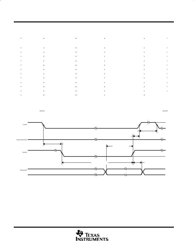
Figure 2. Configuration Cycle Timing
6 |
POST OFFICE BOX 655303 •DALLAS, TEXAS 75265 |

TLV1562 2.7 V TO 5.5 V, HIGH-SPEED LOW-POWER RECONFIGURABLE ANALOG-TO-DIGITAL CONVERTER WITH 4-INPUT, DUAL S/H, PARALLEL INTERFACE, AND POWER DOWN
SLAS162 ± SEPTEMBER 1998
detailed description (continued)
The following examples show how to program configuration registers CR0 and CR1 for different settings.
Example 1:
REGISTER |
INDEX |
|
|
|
|
|
|
|
|
COMMENT |
||||||
|
|
|
|
|
|
|
|
|
|
|
||||||
D9 |
D8 |
|
D7 |
D6 |
D5 |
D4 |
D3 |
D2 |
D1 |
D0 |
||||||
|
|
|
|
|
|
|
||||||||||
|
|
|
|
|
|
|
|
|
|
|
|
|
|
|
|
|
|
|
|
|
|
|
|
|
|
|
|
|
|
|
|
||
CR0 |
0 |
0 |
|
1 |
1 |
0 |
1 |
0 |
0 |
0 |
0 |
Mono interrupt mode, use |
RD, |
write 0D0h to ADC |
||
|
|
|
|
|
|
|
|
|
|
|
|
|
|
|
|
|
CR1 |
0 |
1 |
|
0 |
0 |
0 |
0 |
0 |
0 |
0 |
0 |
Use 2s complementary output, use |
|
write 104h to ADC |
||
|
RD, |
|||||||||||||||
Example 2:
|
|
|
|
|
|
|
|
|
|
|
|
|
|
CR0 |
0 |
0 |
1 |
1 |
0 |
1 |
0 |
0 |
0 |
0 |
Mono interrupt mode, use CSTART, write 0D0h to ADC |
||
|
|
|
|
|
|
|
|
|
|
|
|
|
|
CR1 |
0 |
1 |
0 |
1 |
0 |
0 |
0 |
0 |
0 |
0 |
Use 2s complementary output, write 144h to ADC |
||
Example 3:
|
|
|
|
|
|
|
|
|
|
|
|
|
|
CR0 |
0 |
0 |
1 |
1 |
0 |
1 |
0 |
1 |
0 |
0 |
Dual interrupt mode, use CSTART only, write 0D4h to ADC |
||
|
|
|
|
|
|
|
|
|
|
|
|
|
|
CR1 |
0 |
1 |
0 |
1 |
0 |
0 |
0 |
0 |
0 |
0 |
Use 2s complementary output, write 144h to ADC |
||
Example 4:
|
|
|
|
|
|
|
|
|
|
|
|
|
|
CR0 |
0 |
0 |
1 |
1 |
0 |
1 |
1 |
0 |
0 |
0 |
Mono continuous mode, use RD only, write 0D8h to ADC |
||
|
|
|
|
|
|
|
|
|
|
|
|
|
|
CR1 |
0 |
1 |
0 |
0 |
0 |
0 |
0 |
0 |
0 |
0 |
Use 2s complementary output, write 104h to ADC |
||
Example 5:
|
|
|
|
|
|
|
|
|
|
|
|
|
|
CRO |
0 |
0 |
1 |
1 |
0 |
1 |
1 |
1 |
0 |
0 |
Dual continuous mode, use RD only, write 0DCh to ADC |
||
|
|
|
|
|
|
|
|
|
|
|
|
|
|
CR1 |
0 |
1 |
0 |
0 |
0 |
0 |
0 |
1 |
0 |
0 |
Binary output, write 104h to ADC |
||
analog input
input types
The four analog inputs can be configured as two pairs of differential inputs or four single-ended inputs by setting the control register 0 bit 4 input type selection (dual or single channel).
differential input (CR0.4=1)
Up to two channels are available when the TLV1562 is programmed for differential input. The output data format is bipolar when the device is operated in differential input mode.
single-ended input (CR0.4=0)
Up to four channels are available when the TLV1562 is programmed for single-ended input. The output data format is unipolar when the device is operated in single-ended input mode.
POST OFFICE BOX 655303 •DALLAS, TEXAS 75265 |
7 |
TLV1562
2.7 V TO 5.5 V, HIGH-SPEED LOW-POWER RECONFIGURABLE ANALOG-TO-DIGITAL CONVERTER WITH 4-INPUT, DUAL S/H, PARALLEL INTERFACE, AND POWER DOWN
SLAS162 ± SEPTEMBER 1998
detailed description (continued)
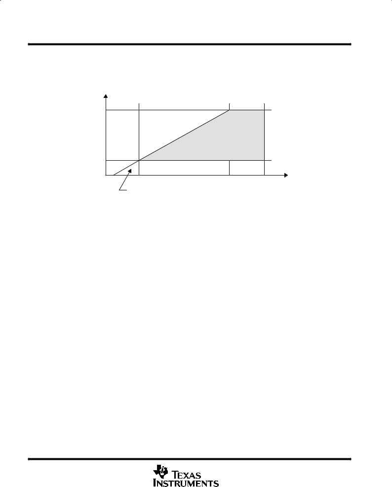
input signal range
The analog input signal range for a specific supply voltage AVDD ranges from (AVDD ± 1.9 V) to 0.8 V.
VSWING |
|
|
3 V |
|
|
0.8 V |
|
|
2.7 |
4.9 |
AVDD (V) |
5.5 |
Linearity not Guaranteed
Limited by Noise
Figure 3. Analog Input Range vs AVDD
VREFCM + 0.5 × VSWING ≤ AVDD ±1 V
VREFCM ± 0.5 × VSWING ≥ 0.8 V
Where:
VREFCM = (VREFP + VREFM)/2 is the common mode reference voltage.
VSWING = dynamic range of the input signal,
VSWING = VINP ± VINM,
And the common mode input voltage is:
VINCM = (VINP + VINM)/2,
MAX VSWING = MIN [(AVDD ± 1.9 V), 3 V]
For single-ended input, the analog input range is between VREFP and VREFM. So the range of single-ended VIN is:
3 V if AVDD = 3 V
1 V if AVDD = 3 V
0.8 V if AVDD = 2.7 V
For differential input, the input common mode voltage VINCM can be between AVDD and AGND as long as 3 V ≥ (VINP±VINM) ≥ 0.8 V.
This means VINCM ≥ 0.4 V.
So the range of differential analog input voltage, (VINP±VINM) is:
3 V if AVDD = 3 V
1 V if AVDD = 3 V
0.8 V if AVDD = 2.7 V
8 |
POST OFFICE BOX 655303 •DALLAS, TEXAS 75265 |

TLV1562 2.7 V TO 5.5 V, HIGH-SPEED LOW-POWER RECONFIGURABLE ANALOG-TO-DIGITAL CONVERTER WITH 4-INPUT, DUAL S/H, PARALLEL INTERFACE, AND POWER DOWN
|
|
|
|
SLAS162 ± SEPTEMBER 1998 |
detailed description (continued) |
|
|
||
equivalent input impedance |
|
|
||
|
|
|
Ron(Ω) |
|
|
|
FB |
1 k |
|
|
|
|
|
|
Rs |
Ron |
Ron |
|
|
Vin |
|
|
|
|
|
|
0 V |
|
|
|
|
Buffer |
|
|
Cpad = 10 pF |
|
Csample = 0.5 pF |
0.5 k |
|
|
|
|
||
|
|
|
2.7 |
VCC (V) |
|
|
|
5.5 |
|
Figure 4. Equivalent Input Circuit |
Figure 5. Input Mux On Resistance vs |
|
Analog Supply Voltage |
||
|
Req = Vin/Ieq = (Q/Cin)/(Q/T) = T/Cin = 1/(fs × Csample) = 1/(2 MHz × 0.5 pF) = 1 MΩ
Where fs is the sampling frequency, and fc is the conversion frequency
fs = fc/5 |
when the device is in one channel/continuous conversion mode, |
fs = fc/10 |
when the device is in one channel/continuous conversion mode, |
fs = Conversion trigger strobe frequency when the device is in interrupt mode (RD or CSTART) Csample = Input capacitance = 0.5 pF
Cparasitic = Parasitic capacitance = 0.5 pF
Cpad = Input PAD capacitance = 10 pF
Ron = Mux switch on series resistance = 1 kΩ at 2.7 V
Rs = Source output resistance = 1 kΩ
input bandwidth (full power 0 dB input, BW at ±1 dB)
Attenuation in dB
0
±1
±2
±3
±4
±5
10 |
20 |
30 |
40 |
50 |
60 |
70 |
80 |
90 |
100 |
110 |
120 |
130 |
140 |
150 |
Analog Input Frequency ± MHz |
|
BW = 1/[2 × π × (Rtotal y Cac)] |
|
= 1/[2 × π × ((Ron + Rs) × (Csample + Cparasitic))] |
|
= 1/[2 × π × (2K × 1 pF)] |
|
= 79.6 MHz |
(Theoretical Max) |
Figure 6. Typical Analog Input Frequency Input Bandwidth
POST OFFICE BOX 655303 •DALLAS, TEXAS 75265 |
9 |
TLV1562
2.7 V TO 5.5 V, HIGH-SPEED LOW-POWER RECONFIGURABLE ANALOG-TO-DIGITAL CONVERTER WITH 4-INPUT, DUAL S/H, PARALLEL INTERFACE, AND POWER DOWN
SLAS162 ± SEPTEMBER 1998
reference voltage inputs
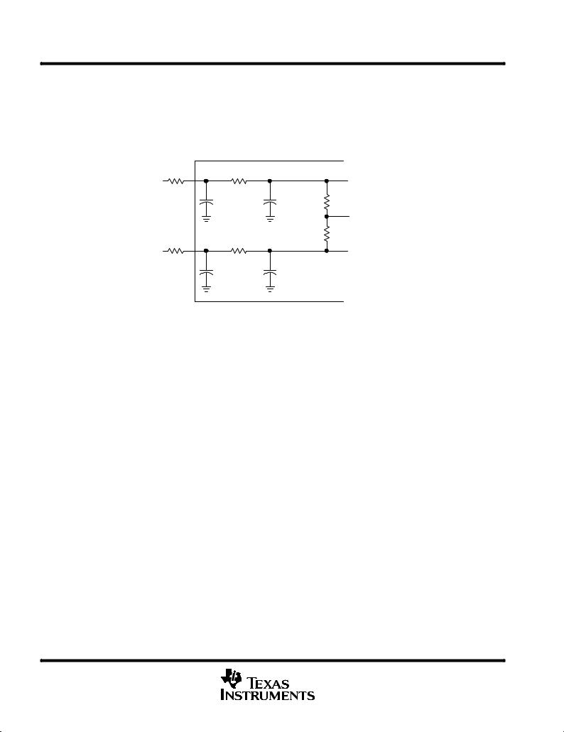
The TLV1562 has two reference input pins: REFP and REFM. The voltage levels applied to these pins establish the upper and lower limits of the analog inputs to produce a full-scale and zero-scale reading respectively. The values of VREFP, VREFM, and the analog input should not exceed the positive supply or be less than GND consistent with the specified absolute maximum ratings. The digital output is at full scale when the input signal is equal to or higher than VREFP and is at zero when the input signal is equal to or lower than VREFM. The internal resistance from VREFP to VREFM may be as low as 20 kΩ (±10%).
Rs |
Ron |
|
|
VREFP |
|
|
|
|
Cpad |
Cin = 1 pF |
10 kΩ |
|
= 10 pF |
|
VREFCM |
|
|
|
|
Rs |
Ron |
|
10 kΩ |
|
|
||
VREFM |
|
|
|
|
Cpad |
Cin = 1 pF |
|
|
= 10 pF |
|
|
The reference voltages must satisfy the following conditions: VREFP ≤ AVDD ± 1 V,
AGND + 0.9 V < VREFM and
3 V ≥ (VREFP ± VREFM) ≥ 0.8 V
Figure 7. Equivalent Circuit for Reference input
10 |
POST OFFICE BOX 655303 •DALLAS, TEXAS 75265 |
TLV1562 2.7 V TO 5.5 V, HIGH-SPEED LOW-POWER RECONFIGURABLE ANALOG-TO-DIGITAL CONVERTER WITH 4-INPUT, DUAL S/H, PARALLEL INTERFACE, AND POWER DOWN
SLAS162 ± SEPTEMBER 1998
sampling/conversion
All of the sampling, conversion, and data output in the device are started by a trigger. This trigger can be the RD or CSTART signal depending on the mode of conversion and configuration. The falling edge of the RD signal and the rising edge of the CSTART signal are extremely important since they are used to start the conversion. These edges need to stay as close to the falling edges of the external clock, if they are used as SYSCLK. The minimum setup time with respect to the rising edge of the external SYSCLK should be 5 ns minimum. When the internal SYSCLK is used, this is not an issue, since these two edges start the internal clock automatically; therefore, the setup time is always met.
USING EXTERNAL CLOCK
|
S/H Hold Time |
|
|
EXTERNAL |
|
VIH |
|
|
|
|
|
SYSCLK |
|
VIL |
|
|
|
|
|
td(ECLKL-TRGL) |
ts(TRGL-ECLKH) |
|
|
|
VIH |
|
|
|
Conversion Starts |
|
|
RD |
Next Sampling Starts |
|
|
|
VIL |
|
|
|
|
|
|
|
|
VIH |
|
CSTART |
Conversion Starts |
Next Sampling Starts |
|
|
Sampling Period |
VIL |
|
|
|
|
|
Figure 8. Conversion Trigger Timing ± External Clock |
|
||
USING INTERNAL CLOCK |
|
|
|
|
INTERNAL |
|
|
|
CLOCK STARTS |
|
|
RD |
Conversion Starts |
Next Sampling Starts |
VIH |
|
|||
td(TRGL-ICLKH) |
|
|
VIL |
|
|
|
|
|
Conversion Starts |
|
VIH |
CSTART |
Next Sampling |
|
|
|
VIL |
||
|
|
||
|
|
Starts |
|
|
|
|
|
S/H Hold Time |
|
|
|
INTERNAL |
|
|
VIH |
SYSCLK |
|
|
VIL |
|
|
|
|
Figure 9. Conversion Trigger Timing ± Internal Clock
POST OFFICE BOX 655303 •DALLAS, TEXAS 75265 |
11 |

TLV1562
2.7 V TO 5.5 V, HIGH-SPEED LOW-POWER RECONFIGURABLE ANALOG-TO-DIGITAL CONVERTER WITH 4-INPUT, DUAL S/H, PARALLEL INTERFACE, AND POWER DOWN
SLAS162 ± SEPTEMBER 1998
Table 2. Conversion Trigger Edge
CONVERSION |
|
CONVERSION |
|
|
START OF |
|
START OF |
CONVERSION |
CONVERSION |
|
INTERRUPT |
|
|
|
|
|||||||||||
|
|
|
|
TIME |
TIME |
|
CANCELED |
DATA OUT |
||||||||||||||||||
MODE |
|
TRIGGER |
|
|
SAMPLING |
|
CONVERSION |
|
||||||||||||||||||
|
|
|
|
(INTERNAL CLK) |
(EXTERNAL CLK) |
|
|
|
BY |
|
|
|
|
|||||||||||||
|
|
|
|
|
|
|
|
|
|
|
|
|
|
|
|
|
|
|
|
|
|
|
||||
|
|
|
|
|
|
|
|
|
|
|
|
|
|
|
|
|
|
|
|
|
|
|
|
|
|
|
Mono |
|
|
|
|
|
|
↑³ or |
|
|
↓ |
6 SYSCLK |
5 SYSCLK |
|
|
↑ |
41 ns§ from |
|
|
low |
|||||||
|
RD |
|
|
|
WR |
|
RD |
|
RD |
INT |
||||||||||||||||
Interrupt |
|
|
|
|
|
2 SYSCLK from |
RD |
↓ |
|
|
|
|
|
|
|
|
|
|
|
|
|
|
|
|||
|
|
|
|
|
|
|
|
|
|
|
|
|
|
|
|
|
||||||||||
|
|
|
|
² |
|
|
|
↓ |
|
|
|
↑ |
6 SYSCLK |
5 SYSCLK |
|
|
↓ |
41 ns§ from |
|
low |
||||||
|
|
CSTART |
|
CSTART |
|
CSTART |
|
RD |
RD |
|||||||||||||||||
Dual |
|
|
|
|
|
|
|
|
↓ |
|
|
|
↑ |
12 SYSCLK |
10 SYSCLK |
First |
|
↓ |
41 ns§ from |
|
low |
|||||
|
CSTART |
|
|
CSTART |
|
CSTART |
RD |
RD |
||||||||||||||||||
Interrupt |
|
|
|
|
|
|
|
|
|
|
|
|
|
|
|
|
|
|
|
|
|
|
|
|
|
|
|
|
|
|
|
|
|
|
|
|
|
|
|
|
|||||||||||||
Mono |
|
|
|
|
|
|
|
↑³ or |
|
|
↓ |
6 SYSCLK |
5 SYSCLK |
N/A |
41 ns§ from |
|
low |
|||||||||
|
RD |
|
WR |
|
RD |
RD |
||||||||||||||||||||
Continuous |
|
|
|
|
|
2 SYSCLK from |
RD |
↓ |
|
|
|
|
|
|
|
|
|
|
|
|
|
|
|
|||
|
|
|
|
|
|
|
|
|
|
|
|
|||||||||||||||
Dual |
|
|
|
|
|
|
|
↑³ or |
|
|
↓ |
12 SYSCLK |
10 SYSCLK |
N/A |
41 ns§ from |
|
low |
|||||||||
|
RD |
|
WR |
|
RD |
RD |
||||||||||||||||||||
Continuous |
|
|
|
|
|
7 SYSCLK from |
RD |
↓ |
|
|
|
|
|
|
|
|
|
|
|
|
|
|
|
|||
|
|
|
|
|
|
|
|
|
|
|
|
|
|
|
|
|
|
|
|
|
|
|
|
|
|
|
² CSTART works with or without CS active.
³The first sampling period starts at the last RD low of the previous cycle or WR high of the configuration cycle. RD low is the falling edge of RD and WR high is the rising edge of the WR signal. (Minimum sample/hold amp settling time = one SYSCLK, approximately 100 ns min, at Rs ≤ 1 kΩ).
§Output data enable time is dependent on bus loading and supply voltage (BDVDD). For BDVDD = 5 V, the enable time is 19 ns at 25 pF, 23 ns at 50 pF, and 25 ns at 100 pF. For BDVDD = 2.7 V, the enable time is 37 ns at 25 pF, 41 ns at 50 pF, and 56 ns at 100 pF.
The TLV1562 provides four types of conversion modes. The two interrupt-driven conversion modes are asynchronous and are simple one-shot conversions. The auto-powerdown conversion feature can be enabled when interrupt-driven conversion modes are used. The other two continuous conversion modes are synchronous with the RD signal (as a clock) from the processor and are more suitable for repetitive signal measurement. These different modes of conversion offer a tradeoff between simplicity and speed.
12 |
POST OFFICE BOX 655303 •DALLAS, TEXAS 75265 |
 Loading...