


TLV1543MJ
Texas Instruments TLV1543MJ, TLV1543MJB, TLV1543MFKB, TLV1543IDBR, TLV1543IDBLE Datasheet
...
TLV1543C, TLV1543M
3.3-V 10-BIT ANALOG-TO-DIGITAL CONVERTERS
WITH SERIAL CONTROL AND 11 ANALOG INPUTS
SLAS072C – DECEMBER 1992 – REVISED MARCH 1995
1
POST OFFICE BOX 655303 • DALLAS, TEXAS 75265
D
3.3-V Supply Operation
D
10-Bit-Resolution A/D Converter
D
11 Analog Input Channels
D
Three Built-In Self-Test Modes
D
Inherent Sample and Hold
D
Total Unadjusted Error...±1 LSB Max
D
On-Chip System Clock
D
End-of-Conversion (EOC) Output
D
Pin Compatible With TLC1543
D
CMOS Technology
description
The TL V1543C and TL V1543M are CMOS 10-bit,
switched-capacitor, successive-approximation,
analog-to-digital converters. These devices have
three inputs and a 3-state output [chip select (CS
),
input-output clock (I/O CLOCK), address input
(ADDRESS), and data output (DATA OUT)] that
provide a direct 4-wire interface to the serial port
of a host processor. The devices allow high-speed
data transfers from the host.
In addition to a high-speed A/D converter and
versatile control capability , these devices have an
on-chip 14-channel multiplexer that can select
any one of 11 analog inputs or any one of three
internal self-test voltages. The sample-and-hold
function is automatic. At the end of A/D conversion, the end-of-conversion (EOC) output goes high to indicate
that conversion is complete. The converter incorporated in the devices features differential high-impedance
reference inputs that facilitate ratiometric conversion, scaling, and isolation of analog circuitry from logic and
supply noise. A switched-capacitor design allows low-error conversion over the full operating free-air
temperature range.
The TL V1543C is characterized for operation from 0°C to 70°C. The TLV1543M is characterized for operation
over the full military temperature range of –55°C to 125°C.
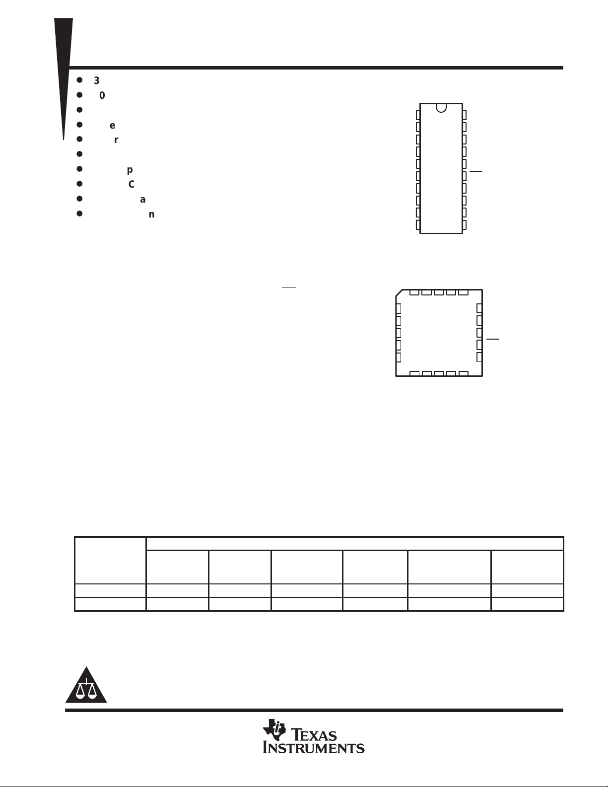
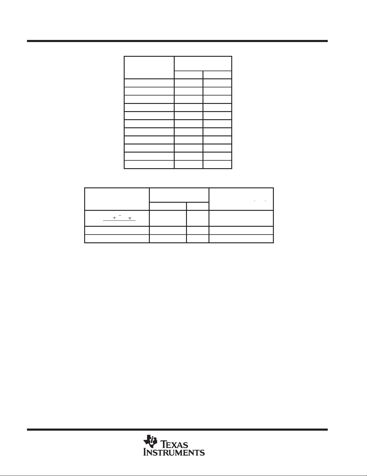
AVAILABLE OPTIONS
PACKAGE
T
A
SMALL
OUTLINE
(DB)
SMALL
OUTLINE
(DW)
CHIP CARRIER
(FK)
CERAMIC DIP
(J)
PLASTIC DIP
(N)
PLASTIC CHIP
CARRIER
(FN)
0°C to 70°C TLV1543CDB TLV1543CDW — — TLV1543CN TLV1543CFN
–55°C to 125°C — — TLV1543MFK TLV1543MJ — —
Copyright 1995, Texas Instruments Incorporated
PRODUCTION DATA information is current as of publication date.
Products conform to specifications per the terms of Texas Instruments
standard warranty. Production processing does not necessarily include
testing of all parameters.
Please be aware that an important notice concerning availability, standard warranty, and use in critical applications of
Texas Instruments semiconductor products and disclaimers thereto appears at the end of this data sheet.
1
2
3
4
5
6
7
8
9
10
20
19
18
17
16
15
14
13
12
11
A0
A1
A2
A3
A4
A5
A6
A7
A8
GND
V
CC
EOC
I/O CLOCK
ADDRESS
DATA OUT
CS
REF+
REF–
A10
A9
DB, DW, FK, J, OR N PACKAGE
(TOP VIEW)
3212019
910111213
4
5
6
7
8
18
17
16
15
14
I/O CLOCK
ADDRESS
DATA OUT
CS
REF+
A3
A4
A5
A6
A7
FN PACKAGE
(TOP VIEW)
A2
A1
A0
A10
REF –
EOC
A8
GND
A9
CC
V
TLV1543C, TLV1543M
3.3-V 10-BIT ANALOG-TO-DIGITAL CONVERTERS
WITH SERIAL CONTROL AND 11 ANALOG INPUTS
SLAS072C – DECEMBER 1992 – REVISED MARCH 1995
2
POST OFFICE BOX 655303 • DALLAS, TEXAS 75265
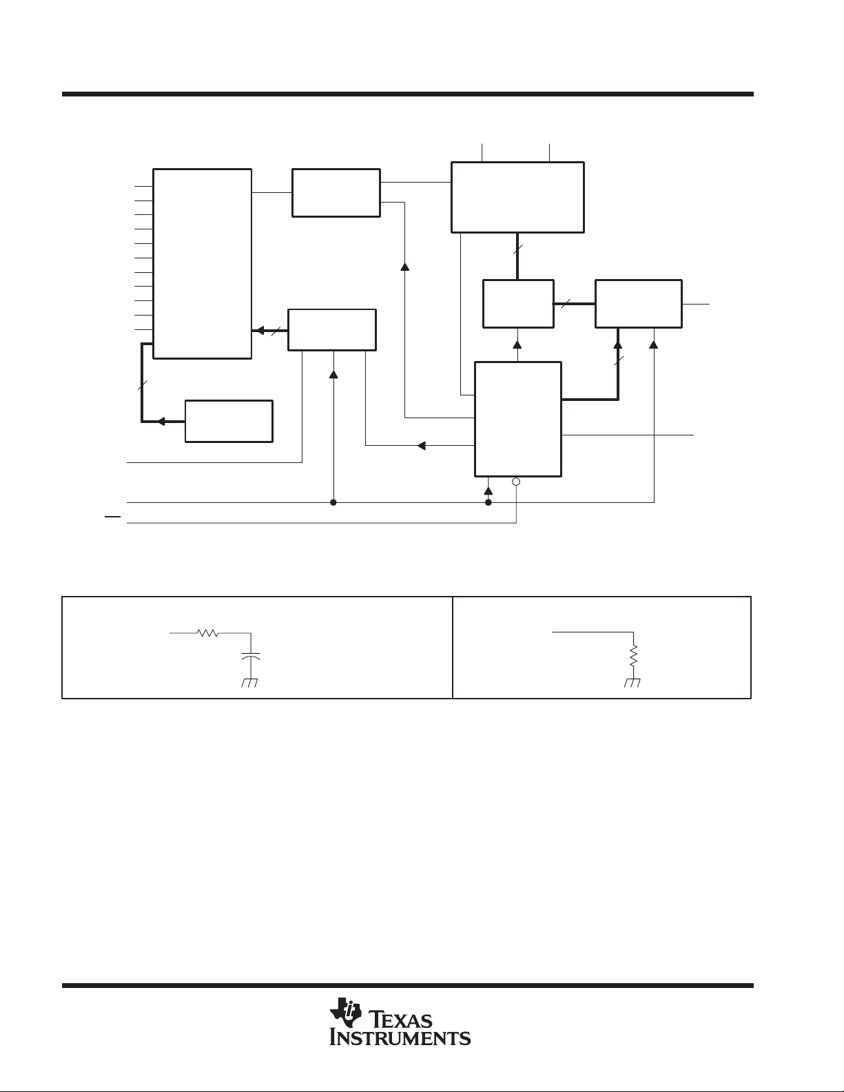
functional block diagram
14-Channel
Analog
Multiplexer
Sample and
Hold
10-Bit
Analog-to-Digital
Converter
(switched capacitors)
Self-Test
Reference
Output
Data
Register
10-to-1 Data
Selector and
Driver
System Clock,
Control Logic,
and I/O
Counters
Input Address
Register
4
10
10
4
REF+ REF–
DATA
OUT
ADDRESS
I/O CLOCK
CS
3
EOC
1
2
3
4
5
6
7
8
9
11
12
A0
A1
A2
A3
A4
A5
A6
A7
A8
A9
A10
14 13
16
19
17
18
15
typical equivalent inputs
INPUT CIRCUIT IMPEDANCE DURING SAMPLING MODE INPUT CIRCUIT IMPEDANCE DURING HOLD MODE
1 kΩ TYP
C
i
= 60 pF TYP
(equivalent input
capacitance)
5 MΩ TYP
A0–A10
A0–A10
TLV1543C, TLV1543M
3.3-V 10-BIT ANALOG-TO-DIGITAL CONVERTERS
WITH SERIAL CONTROL AND 11 ANALOG INPUTS
SLAS072C – DECEMBER 1992 – REVISED MARCH 1995
3
POST OFFICE BOX 655303 • DALLAS, TEXAS 75265
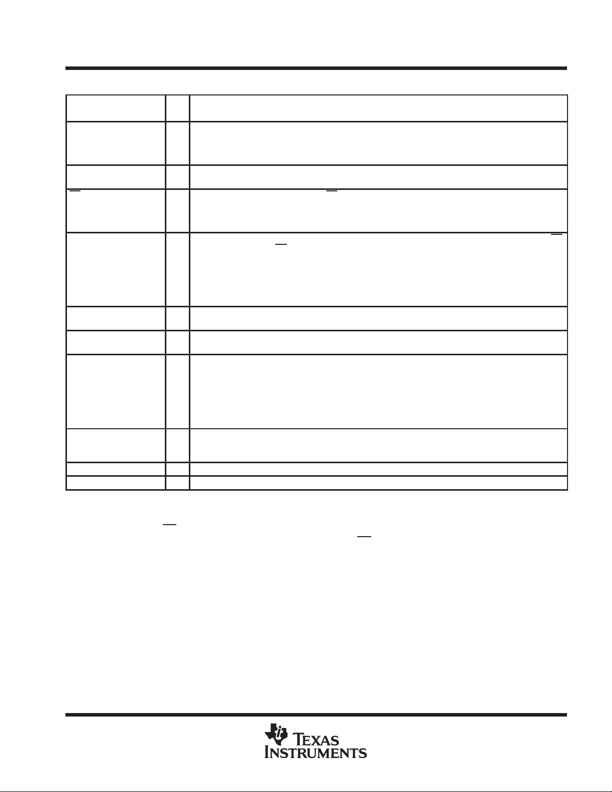
Terminal Functions
TERMINAL
NAME NO.
I/O
DESCRIPTION
ADDRESS 17 I Serial address. A 4-bit serial address selects the desired analog input or test voltage that is to be converted
next. The address data is presented with the MSB first and is shifted in on the first four rising edges of I/O
CLOCK. After the four address bits have been read into the address register, ADDRESS is ignored for the
remainder of the current conversion period.
A0–A10 1–9, 11,
12
I Analog signal. The 11 analog inputs are applied to A0–A10 and are internally multiplexed. The driving source
impedance should be less than or equal to 1 kΩ .
CS 15 I Chip select. A high-to-low transition on CS resets the internal counters and controls and enables DAT A OUT ,
ADDRESS, and I/O CLOCK within a maximum of a setup time plus two falling edges of the internal system
clock. A low-to-high transition disables ADDRESS and I/O CLOCK within a setup time plus two falling edges
of the internal system clock.
DATA OUT 16 O The 3-state serial output for the A/D conversion result. DAT A OUT is in the high-impedance state when CS
is high and active when CS is low. With a valid chip select, DA T A OUT is removed from the high-impedance
state and is driven to the logic level corresponding to the MSB value of the previous conversion result. The
next falling edge of I/O CLOCK drives DAT A OUT to the logic level corresponding to the next most significant
bit, and the remaining bits are shifted out in order with the LSB appearing on the ninth falling edge of I/O
CLOCK. On the tenth falling edge of I/O CLOCK, DATA OUT is driven to a low logic level so that serial
interface data transfers of more than ten clocks produce zeroes as the unused LSBs.
EOC 19 O End of conversion. EOC goes from a high- to a low- logic level on the trailing edge of the tenth I/O CLOCK
and remains low until the conversion is complete and data are ready for transfer.
GND 10 I The ground return terminal for the internal circuitry . Unless otherwise noted, all voltage measurements are
with respect to GND.
I/O CLOCK 18 I Input/output clock. I/O CLOCK receives the serial I/O CLOCK input and performs the following four functions:
1) It clocks the four input address bits into the address register on the first four rising edges of I/O
CLOCK with the multiplex address available after the fourth rising edge.
2) On the fourth falling edge of I/O CLOCK, the analog input voltage on the selected multiplex input begins
charging the capacitor array and continues to do so until the tenth falling edge of I/O CLOCK.
3) It shifts the nine remaining bits of the previous conversion data out on DATA OUT.
4) It transfers control of the conversion to the internal state controller on the falling edge of the tenth clock.
REF+ 14 I The upper reference voltage value (nominally V
CC
) is applied to REF+. The maximum input voltage range
is determined by the difference between the voltage applied to REF+ and the voltage applied to the REF–
terminal.
REF– 13 I The lower reference voltage value (nominally ground) is applied to REF–.
V
CC
20 I Positive supply voltage
detailed description
With chip select (CS) inactive (high), the ADDRESS and I/O CLOCK inputs are initially disabled and DA TA OUT
is in the high-impedance state. When the serial interface takes CS
active (low), the conversion sequence begins
with the enabling of I/O CLOCK and ADDRESS and the removal of DA T A OUT from the high-impedance state.
The host then provides the 4-bit channel address to ADDRESS and the I/O CLOCK sequence to I/O CLOCK.
During this transfer, the host serial interface also receives the previous conversion result from DATA OUT. I/O
CLOCK receives an input sequence that is between 10 and 16 clocks long from the host. The first four I/O clocks
load the address register with the 4-bit address on ADDRESS selecting the desired analog channel and the next
six clocks providing the control timing for sampling the analog input.
TLV1543C, TLV1543M
3.3-V 10-BIT ANALOG-TO-DIGITAL CONVERTERS
WITH SERIAL CONTROL AND 11 ANALOG INPUTS
SLAS072C – DECEMBER 1992 – REVISED MARCH 1995
4
POST OFFICE BOX 655303 • DALLAS, TEXAS 75265
detailed description (continued)
There are six basic serial interface timing modes that can be used with the device. These modes are determined
by the speed of I/O CLOCK and the operation of CS
as shown in T able 1. These modes are (1) a fast mode with
a 10-clock transfer and CS
inactive (high) between conversion cycles, (2) a fast mode with a 10-clock transfer
and CS
active (low) continuously , (3) a fast mode with an 11- to 16-clock transfer and CS inactive (high) between
conversion cycles, (4) a fast mode with a 16-bit transfer and CS
active (low) continuously , (5) a slow mode with
an 11- to 16-clock transfer and CS
inactive (high) between conversion cycles, and (6) a slow mode with a
16-clock transfer and CS
active (low) continuously.
The MSB of the previous conversion appears on DA T A OUT on the falling edge of CS
in mode 1, mode 3, and
mode 5, on the rising edge of EOC in mode 2 and mode 4, and following the 16th clock falling edge in mode 6.
The remaining nine bits are shifted out on the next nine falling edges of I/O CLOCK. Ten bits of data are
transmitted to the host through DA T A OUT. The number of serial clock pulses used also depends on the mode
of operation, but a minimum of ten clock pulses is required for conversion to begin. On the 10th clock falling
edge, the EOC output goes low and returns to the high logic level when conversion is complete and the result
can be read by the host. On the 10th clock falling edge, the internal logic takes DA TA OUT low to ensure that
the remaining bit values are zero if the I/O CLOCK transfer is more than ten clocks long.
T able 1 lists the operational modes with respect to the state of CS
, the number of I/O serial transfer clocks that
can be used, and the timing edge on which the MSB of the previous conversion appears at the output.
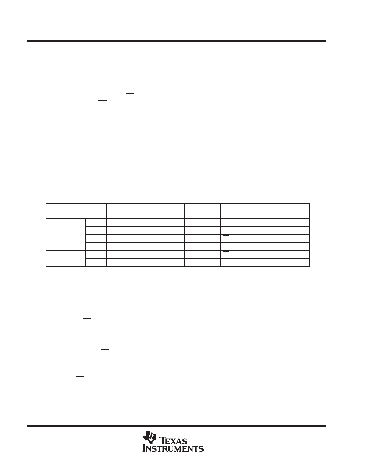
Table 1. Mode Operation
MODES
CS
NO. OF
I/O CLOCKS
MSB AT DATA OUT
†
TIMING
DIAGRAM
Mode 1 High between conversion cycles 10 CS falling edge Figure 9
Mode 2 Low continuously 10 EOC rising edge Figure 10
Fast
Modes
Mode 3 High between conversion cycles 11 to 16
‡
CS falling edge Figure 11
Mode 4 Low continuously 16
‡
EOC rising edge Figure 12
Mode 5 High between conversion cycles 11 to 16
‡
CS falling edge Figure 13
Slo
w
Modes
Mode 6 Low continuously 16
‡
16th clock falling edge Figure 14
†
These edges also initiate serial-interface communication.
‡
No more than 16 clocks should be used.
fast modes
The device is in a fast mode when the serial I/O CLOCK data transfer is completed before the conversion is
completed. With a 10-clock serial transfer, the device can only run in a fast mode since a conversion does not
begin until the falling edge of the 10th I/O CLOCK.
mode 1: fast mode, CS inactive (high) between conversion cycles, 10-clock transfer
In this mode, CS is inactive (high) between serial I/O CLOCK transfers and each transfer is ten clocks long. The
falling edge of CS
begins the sequence by removing DA TA OUT from the high-impedance state. The rising edge
of CS
ends the sequence by returning DA T A OUT to the high-impedance state within the specified delay time.
Also, the rising edge of CS
disables the I/O CLOCK and ADDRESS terminals within a setup time plus two falling
edges of the internal system clock.
mode 2: fast mode, CS active (low) continuously, 10-clock transfer
In this mode, CS is active (low) between serial I/O CLOCK transfers and each transfer is ten clocks long. After
the initial conversion cycle, CS
is held active (low) for subsequent conversions; the rising edge of EOC then
begins each sequence by removing DATA OUT from the low logic level, allowing the MSB of the previous
conversion to appear immediately on this output.
TLV1543C, TLV1543M
3.3-V 10-BIT ANALOG-TO-DIGITAL CONVERTERS
WITH SERIAL CONTROL AND 11 ANALOG INPUTS
SLAS072C – DECEMBER 1992 – REVISED MARCH 1995
5
POST OFFICE BOX 655303 • DALLAS, TEXAS 75265
mode 3: fast mode, CS inactive (high) between conversion cycles, 11- to 16-clock transfer
In this mode, CS is inactive (high) between serial I/O CLOCK transfers and each transfer can be 1 1 to 16 clocks
long. The falling edge of CS
begins the sequence by removing DA T A OUT from the high-impedance state. The
rising edge of CS
ends the sequence by returning DA T A OUT to the high-impedance state within the specified
delay time. Also, the rising edge of CS
disables the I/O CLOCK and ADDRESS terminals within a setup time
plus two falling edges of the internal system clock.
mode 4: fast mode, CS active (low) continuously, 16-clock transfer
In this mode, CS is active (low) between serial I/O CLOCK transfers and each transfer must be exactly 16 clocks
long. After the initial conversion cycle, CS
is held active (low) for subsequent conversions; the rising edge of
EOC then begins each sequence by removing DATA OUT from the low logic level, allowing the MSB of the
previous conversion to appear immediately on this output.
slow modes
In a slow mode, the conversion is completed before the serial I/O CLOCK data transfer is completed. A slow
mode requires a minimum 11-clock transfer into I/O CLOCK, and the rising edge of the eleventh clock must
occur before the conversion period is complete; otherwise, the device loses synchronization with the host serial
interface, and CS
has to be toggled to initialize the system. The eleventh rising edge of the I/O CLOCK must
occur within 9.5 µs after the tenth I/O clock falling edge.
mode 5: slow mode, CS inactive (high) between conversion cycles, 11- to 16-clock transfer
In this mode, CS is inactive (high) between serial I/O CLOCK transfers and each transfer can be 1 1 to 16 clocks
long. The falling edge of CS
begins the sequence by removing DA T A OUT from the high-impedance state. The
rising edge of CS
ends the sequence by returning DA T A OUT to the high-impedance state within the specified
delay time. Also, the rising edge of CS
disables the I/O CLOCK and ADDRESS terminals within a setup time
plus two falling edges of the internal system clock.
mode 6: slow mode, CS active (low) continuously, 16-clock transfer
In this mode, CS is active (low) between serial I/O CLOCK transfers and each transfer must be exactly 16 clocks
long. After the initial conversion cycle, CS
is held active (low) for subsequent conversions. The falling edge of
the sixteenth I/O CLOCK then begins each sequence by removing DA TA OUT from the low state, allowing the
MSB of the previous conversion to appear immediately at DATA OUT. The device is then ready for the next
16-clock transfer initiated by the serial interface.
address bits
The 4-bit analog channel-select address for the next conversion cycle is presented to the ADDRESS terminal
(MSB first) and is clocked into the address register on the first four leading edges of I/O CLOCK. This address
selects one of 14 inputs (11 analog inputs or 3 internal test inputs).
analog inputs and test modes
The 1 1 analog inputs and the 3 internal test inputs are selected by the 14-channel multiplexer according to the
input address as shown in Tables 2 and 3. The input multiplexer is a break-before-make type to reduce
input-to-input noise injection resulting from channel switching.
Sampling of the analog input starts on the falling edge of the fourth I/O CLOCK, and sampling continues for six
I/O CLOCK periods. The sample is held on the falling edge of the tenth I/O CLOCK. The three test inputs are
applied to the multiplexer, sampled, and converted in the same manner as the external analog inputs.
TLV1543C, TLV1543M
3.3-V 10-BIT ANALOG-TO-DIGITAL CONVERTERS
WITH SERIAL CONTROL AND 11 ANALOG INPUTS
SLAS072C – DECEMBER 1992 – REVISED MARCH 1995
6
POST OFFICE BOX 655303 • DALLAS, TEXAS 75265
Table 2. Analog-Channel-Select Address
ANALOG INPUT
VALUE SHIFTED INTO
ADDRESS INPUT
SELECTED
BINARY HEX
A0 0000 0
A1 0001 1
A2 0010 2
A3 0011 3
A4 0100 4
A5 0101 5
A6 0110 6
A7 0111 7
A8 1000 8
A9 1001 9
A10 1010 A
Table 3. Test-Mode-Select Address
INTERNAL SELF-TEST
VALUE SHIFTED INTO
ADDRESS INPUT
OUTPUT RESULT
(
HEX
)
‡
VOLTAGE
SELECTED
†
BINARY HEX
()
V
–V
ref
)
ref
–
2
1011
B
200
V
ref–
1100 C 000
V
ref+
1101 D 3FF
†
V
ref+
is the voltage applied to the REF+ input, and V
ref–
is the voltage applied to the REF–
input.
‡
The output results shown are the ideal values and vary with the reference stability and with
internal offsets.
converter and analog input
The CMOS threshold detector in the successive-approximation conversion system determines each bit by
examining the charge on a series of binary-weighted capacitors (see Figure 1). In the first phase of the
conversion process, the analog input is sampled by closing the S
C
switch and all S
T
switches simultaneously .
This action charges all the capacitors to the input voltage.
In the next phase of the conversion process, all S
T
and S
C
switches are opened and the threshold detector
begins identifying bits by identifying the charge (voltage) on each capacitor relative to the reference (REF–)
voltage. In the switching sequence, ten capacitors are examined separately until all ten bits are identified and
the charge-convert sequence is repeated. In the first step of the conversion phase, the threshold detector looks
at the first capacitor (weight = 512). Node 512 of this capacitor is switched to the REF+ voltage, and the
equivalent nodes of all the other capacitors on the ladder are switched to REF–. If the voltage at the summing
node is greater than the trip point of the threshold detector (approximately one-half the V
CC
voltage), a bit 0 is
placed in the output register and the 512-weight capacitor is switched to REF–. If the voltage at the summing
node is less than the trip point of the threshold detector, a bit 1 is placed in the register and the 512-weight
capacitor remains connected to REF+ through the remainder of the successive-approximation process. The
process is repeated for the 256-weight capacitor, the 128-weight capacitor, and so forth down the line until all
bits are counted.
With each step of the successive-approximation process, the initial charge is redistributed among the
capacitors. The conversion process relies on charge redistribution to count and weigh the bits from MSB to LSB.
 Loading...