


Texas Instruments TLV5614IPWR, TLV5614IPW, TLV5614IDR, TLV5614CPWR, TLV5614ID Datasheet
...TLV5614 2.7-V TO 5.5-V 12-BIT 3- S QUADRUPLE DIGITAL-TO-ANALOG CONVERTERS
WITH POWER DOWN
SLAS188 ± SEPTEMBER 1998
DFour 12-Bit D/A Converters
DProgrammable Settling Time of Either 3 µs or 9 µs Typ
DTMS320, (Q)SPI, and Microwire Compatible Serial Interface
DInternal Power-On Reset
DLow Power Consumption:
8 mW, Slow Mode ± 5-V Supply
3.6 mW, Slow Mode ± 3-V Supply
DReference Input Buffer
DVoltage Output Range . . . 2 × the Reference
Input Voltage
DMonotonic Over Temperature
description
DDual 2.7-V to 5.5-V Supply (Separate Digital and Analog Supplies)
DHardware Power Down (10 nA)
DSoftware Power Down (10 nA)
DSimultaneous Update
applications
DBattery Powered Test Instruments
DDigital Offset and Gain Adjustment
DIndustrial Process Controls
DMachine and Motion Control Devices
DCommunications
DArbitrary Waveform Generation
D OR PW PACKAGE
(TOP VIEW)
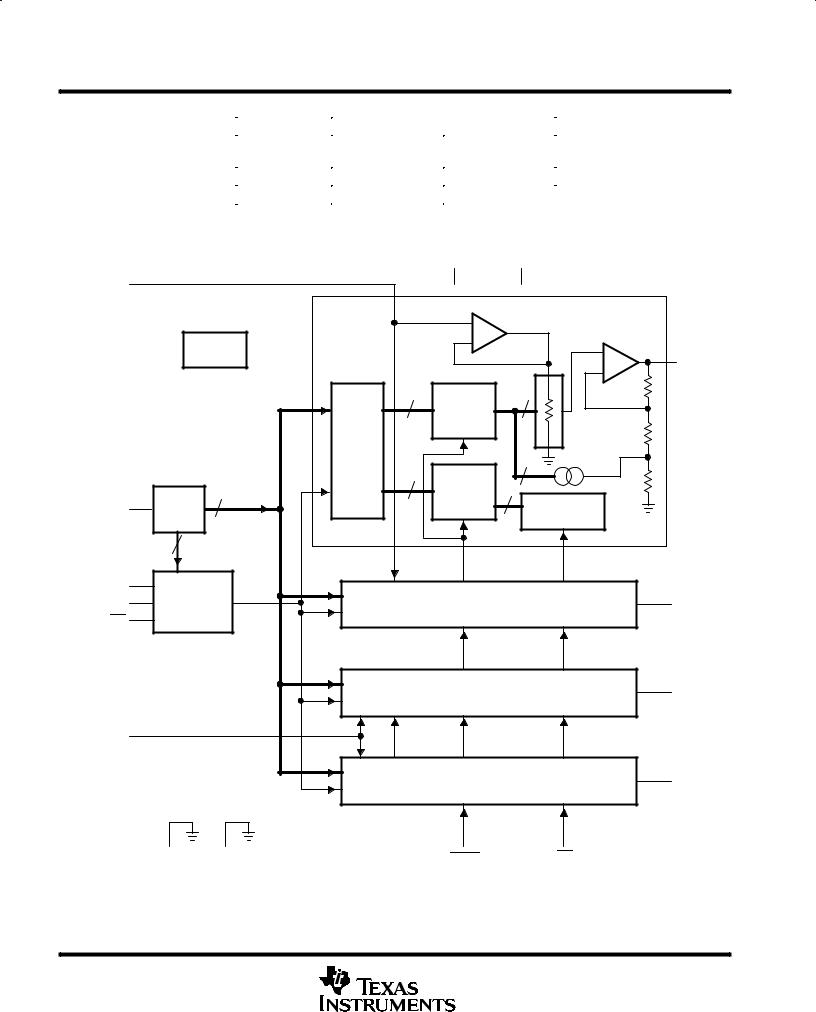
The TLV5614 is a quadruple 12-bit voltage output |
DVDD |
|
|
|
|
AVDD |
|||
|
|
|
|
||||||
digital-to-analog converter (DAC) with a flexible |
|
1 |
16 |
|
|||||
|
|
|
|
||||||
4-wire serial interface. The 4-wire serial interface |
|
|
PD |
|
2 |
15 |
|
REFINAB |
|
allows glueless interface to TMS320, SPI, QSPI, |
|
LDAC |
|
|
3 |
14 |
|
OUTA |
|
|
|
|
|
||||||
and Microwire serial ports. The TLV5614 is |
|
DIN |
|
4 |
13 |
|
OUTB |
||
|
|
|
|||||||
programmed with a 16-bit serial word comprised |
|
SCLK |
|
5 |
12 |
|
OUTC |
||
|
|
|
|||||||
of a DAC address, individual DAC control bits, and |
|
|
CS |
|
|
6 |
11 |
|
OUTD |
|
|
|
|
|
|||||
a 12-bit DAC value. The device has provision for |
|
|
FS |
|
7 |
10 |
|
REFINCD |
|
|
|
|
|
||||||
two supplies: one digital supply for the serial |
DGND |
|
8 |
9 |
|
AGND |
|||
|
|
||||||||
interface (via pins DVDD and DGND), and one for |
|
|
|
|
|
|
|
|
|
|
|
|
|
|
|
|
|
|
|
the DACs, reference buffers, and output buffers (via pins AVDD and AGND). Each supply is independent of the other, and can be any value between 2.7 V and 5.5 V. The dual supplies allow a typical application where the DAC will be controlled via a microprocessor operating on a 3 V supply (also used on pins DVDD and DGND), with the DACs operating on a 5 V supply. Of course, the digital and anlog supplies can be tied together.
The resistor string output voltage is buffered by a x2 gain rail-to-rail output buffer. The buffer features a Class AB output stage to improve stability and reduce settling time. A rail-to-rail output stage and a power-down mode makes it ideal for single voltage, battery based applications. The settling time of the DAC is programmable to allow the designer to optimize speed versus power dissipation. The settling time is chosen by the control bits within the 16-bit serial input string. A high-impedance buffer is integrated on the REFINAB and REFINCD terminals to reduce the need for a low source impedance drive to the terminal. REFINAB and REFINCD allow DACs A and B to have a different reference voltage then DACs C and D.
The TLC5614 is implemented with a CMOS process and is available in a 16-terminal SOIC package. The TLV5614C is characterized for operation from 0°C to 70°C. The TLV5614I is characterized for operation from ±40°C to 85°C.
Please be aware that an important notice concerning availability, standard warranty, and use in critical applications of Texas Instruments semiconductor products and disclaimers thereto appears at the end of this data sheet.
PRODUCTION DATA information is current as of publication date. Products conform to specifications per the terms of Texas Instruments standard warranty. Production processing does not necessarily include testing of all parameters.
Copyright 1998, Texas Instruments Incorporated
POST OFFICE BOX 655303 •DALLAS, TEXAS 75265 |
1 |
TLV5614
2.7-V TO 5.5-V 12-BIT 3- S QUADRUPLE DIGITAL-TO-ANALOG CONVERTERS
WITH POWER DOWN
SLAS188 ± SEPTEMBER 1998
AVAILABLE OPTIONS
|
|
PACKAGE |
|
TA |
|
|
|
SOIC |
|
TSSOP |
|
|
(D) |
|
(PW) |
|
|
|
|
0°C to 70°C |
TLV5614CD |
|
TLV5614CPW |
|
|
|
|
± 40°C to 85°C |
TLV5614ID |
|
TLV5614IPW |
|
|
|
|
functional block diagram |
|
|
|
|
|
|||
|
|
|
|
|
AVDD |
DVDD |
|
|
REFINAB |
15 |
|
|
|
16 |
1 |
|
|
|
|
|
|
|
|
|
|
|
|
|
|
|
|
|
DAC A |
|
|
|
|
|
|
|
+ |
|
|
|
|
|
Power-On |
|
_ |
|
|
|
|
|
|
|
|
+ |
|
14 |
||
|
|
Reset |
|
|
|
|||
|
|
|
|
|
|
_ |
|
OUTA |
|
|
|
|
|
|
|
|
|
|
|
|
|
12 |
12-Bit |
10 |
|
|
|
|
|
|
|
DAC |
|
|
|
|
|
|
14-Bit |
|
Latch |
|
|
|
|
|
|
|
|
|
|
|
|
|
|
|
Data |
|
|
|
|
|
|
|
|
and |
|
|
2 |
|
|
|
|
|
Control |
2 |
2-Bit |
|
|
|
|
|
|
Register |
|
Control |
2 |
|
|
|
4 |
Serial |
14 |
|
Data |
|
|
|
|
|
|
Power-Down/ |
|
|
|||
DIN |
Input |
|
|
Latch |
|
|
||
|
|
|
|
|
||||
|
|
|
Speed Control |
|
|
|||
|
|
Register |
|
|
|
|
|
|
|
|
|
|
|
|
|
|
|
|
|
2 |
|
|
|
|
|
|
FS |
7 |
DAC Select/ |
|
|
|
|
|
|
5 |
|
|
|
13 |
|
|||
SCLK |
Control |
|
DAC B |
|
OUTB |
|||
6 |
|
|
|
|||||
CS |
Logic |
|
|
|
|
|
|
|
|
|
|
|
|
|
|
|
|
|
|
|
|
|
DAC C |
|
12 |
OUTC |
|
|
|
|
|
|
|
||
REFINCD |
10 |
|
|
|
|
|
|
|
|
|
|
|
|
|
|
|
|
|
|
|
|
|
DAC D |
|
11 |
OUTD |
|
|
|
|
|
|
|
||
|
|
|
|
|
3 |
2 |
|
|
|
|
9 |
8 |
|
|
|
|
|
|
|
AGND |
DGND |
|
LDAC |
PD |
|
|
2 |
POST OFFICE BOX 655303 •DALLAS, TEXAS 75265 |
TLV5614 2.7-V TO 5.5-V 12-BIT 3- S QUADRUPLE DIGITAL-TO-ANALOG CONVERTERS
WITH POWER DOWN
SLAS188 ± SEPTEMBER 1998
|
|
|
|
|
|
|
Terminal Functions |
|
|
|
|
|
|
|
|
|
|
|
|
TERMINAL |
I/O |
|
|
DESCRIPTION |
||
|
NAME |
NO. |
|
|
||||
|
|
|
|
|
||||
|
|
|
|
|
|
|
|
|
|
AGND |
9 |
|
Analog ground |
||||
|
|
|
|
|
|
|
|
|
|
AVDD |
16 |
|
Analog supply |
||||
|
|
|
|
6 |
I |
Chip select. This terminal is active low. |
||
|
CS |
|
|
|||||
|
|
|
|
|
|
|
|
|
|
DGND |
8 |
|
Digital ground |
||||
|
|
|
|
|
|
|
|
|
|
DIN |
4 |
I |
Serial data input |
||||
|
|
|
|
|
|
|
|
|
|
DVDD |
1 |
|
Digital supply |
||||
|
FS |
7 |
I |
Frame sync input. The falling edge of the frame sync pulse indicates the start of a serial data frame shifted out to |
||||
|
|
|
the TLV5614. |
|||||
|
|
|
|
|
|
|||
|
|
|
|
|
|
|
|
|
|
|
|
|
2 |
I |
Power down pin. Powers down all DACs (overriding their individual power down settings), and all output stages. |
||
|
PD |
|||||||
|
|
|
This terminal is active low. |
|||||
|
|
|
|
|
|
|||
|
|
|
|
|
|
|
||
|
|
|
|
3 |
I |
Load DAC. When the |
|
signal is high, no DAC output updates occur when the input digital data is read into |
|
|
|
|
LDAC |
||||
|
LDAC |
|||||||
|
|
|
the serial interface. The DAC outputs are only updated when LDAC is low. |
|||||
|
|
|
|
|
|
|||
|
|
|
|
|
||||
|
REFINAB |
15 |
I |
Voltage reference input for DACs A and B. |
||||
|
|
|
|
|
||||
|
REFINCD |
10 |
I |
Voltage reference input for DACs C and D. |
||||
|
|
|
|
|
||||
|
SCLK |
5 |
I |
Serial Clock input |
||||
|
|
|
|
|
||||
|
OUTA |
14 |
O |
DACA output |
||||
|
|
|
|
|
||||
|
OUTB |
13 |
O |
DACB output |
||||
|
|
|
|
|
||||
|
OUTC |
12 |
O |
DACC output |
||||
|
|
|
|
|
||||
|
OUTD |
11 |
O |
DACD output |
||||
absolute maximum ratings over operating free-air temperature range (unless otherwise noted)²
Supply voltage, (DVDD, AVDD to GND) . . . . . . . . . . . . . . . . . . . . . . . . . . . . . . . . . . . . . . . |
. . . . . . . . . . . . . . . . . 7 |
V |
Supply voltage difference, (AVDD to DVDD) . . . . . . . . . . . . . . . . . . . . . . . . . . . . . . . . . . . |
. . . . . . . ±2.8 V to 2.8 |
V |
Digital input voltage range . . . . . . . . . . . . . . . . . . . . . . . . . . . . . . . . . . . . . . . . . . . . . . . . . |
±0.3 V to DVDD + 0.3 |
V |
Reference input voltage range . . . . . . . . . . . . . . . . . . . . . . . . . . . . . . . . . . . . . . . . . . . . . . |
±0.3 V to AVDD + 0.3 |
V |
Operating free-air temperature range, TA: TLV5614C . . . . . . . . . . . . . . . . . . . . . . . . . . |
. . . . . . . . . 0°C to 70°C |
|
TLV5614I . . . . . . . . . . . . . . . . . . . . . . . . . . . |
. . . . . . . ±40°C to 85°C |
|
Storage temperature range, Tstg . . . . . . . . . . . . . . . . . . . . . . . . . . . . . . . . . . . . . . . . . . . . . |
. . . . . . ±65°C to 150°C |
|
Lead temperature 1,6 mm (1/16 inch) from case for 10 seconds . . . . . . . . . . . . . . . . . |
. . . . . . . . . . . . . . 260°C |
|
²Stresses beyond those listed under ªabsolute maximum ratingsº may cause permanent damage to the device. These are stress ratings only, and functional operation of the device at these or any other conditions beyond those indicated under ªrecommended operating conditionsº is not implied. Exposure to absolute-maximum-rated conditions for extended periods may affect device reliability.
POST OFFICE BOX 655303 •DALLAS, TEXAS 75265 |
3 |

TLV5614
2.7-V TO 5.5-V 12-BIT 3- S QUADRUPLE DIGITAL-TO-ANALOG CONVERTERS
WITH POWER DOWN
SLAS188 ± SEPTEMBER 1998
recommended operating conditions
|
|
MIN |
NOM |
MAX |
UNIT |
|
|
|
|
|
|
|
|
Supply voltage, AVDD, DVDD |
5-V supply |
4.5 |
5 |
5.5 |
V |
|
|
|
|
|
|||
3-V supply |
2.7 |
3 |
3.3 |
|||
|
|
|||||
|
|
|
|
|
|
|
High-level digital input, VIH |
DVDD = 2.7 V to 5.5 V |
2 |
|
|
V |
|
Low-level digital input, VIL |
DVDD = 2.7 V to 5.5 V |
|
|
0.8 |
V |
|
Reference voltage, Vref to REFINAB, REFINCD terminal |
5-V supply, See Note 1 |
0 |
2.048 |
VDD±1.5 |
V |
|
3-V supply, See Note 1 |
0 |
1.024 |
VDD±1.5 |
|||
|
|
|||||
Load resistance, RL |
|
2 |
10 |
|
kΩ |
|
Load capacitance, CL |
|
|
|
100 |
pF |
|
Serial clock rate, SCLK |
|
|
|
20 |
MHz |
|
|
|
|
|
|
|
|
Operating free-air temperature |
TLV5614C |
0 |
|
70 |
°C |
|
|
|
|
|
|||
TLV5614I |
±40 |
|
85 |
|||
|
|
|
NOTE 1: Voltages greater than AVDD/2 will cause output saturation for large DAC codes.
electrical characteristics over recommended operating free-air temperature range, supply voltages, and reference voltages (unless otherwise noted)
static DAC specifications
|
PARAMETER |
TEST CONDITIONS |
MIN TYP |
MAX |
UNIT |
|
|
|
|
|
|
|
|
|
Resolution |
|
12 |
|
bits |
|
|
|
|
|
|
|
|
|
Integral nonlinearity (INL), end point adjusted |
See Note 2 |
±1.5 |
±4 |
LSB |
|
|
|
|
|
|
|
|
|
Differential nonlinearity (DNL) |
See Note 3 |
±0.5 |
±1 |
LSB |
|
|
|
|
|
|
|
|
EZS |
Zero scale error (offset error at zero scale) |
See Note 4 |
|
±12 |
mV |
|
|
Zero scale error temperature coefficient |
See Note 5 |
10 |
|
ppm/°C |
|
|
|
|
|
|
|
|
EG |
Gain error |
See Note 6 |
|
±0.6 |
% of FS |
|
|
voltage |
|||||
|
|
|
|
|
|
|
|
Gain error temperature coefficient |
See Note 7 |
10 |
|
ppm/°C |
|
|
|
|
|
|
|
|
PSRR |
Power supply rejection ratio |
Zero scale |
See Notes 8 and 9 |
± 80 |
|
dB |
|
|
|
|
|||
Full scale |
± 80 |
|
dB |
|||
|
|
|
|
|||
NOTES: 2. The relative accuracy or integral nonlinearity (INL) sometimes referred to as linearity error, is the maximum deviation of the output from the line between zero and full scale excluding the effects of zero code and full-scale errors.
3.The differential nonlinearity (DNL) sometimes referred to as differential error, is the difference between the measured and ideal 1 LSB amplitude change of any two adjacent codes. Monotonic means the output voltage changes in the same direction (or remains constant) as a change in the digital input code.
4.Zero-scale error is the deviation from zero voltage output when the digital input code is zero.
5.Zero-scale-error temperature coefficient is given by: EZS TC = [EZS (Tmax) ± EZS (Tmin)]/Vref × 106/(Tmax ± Tmin).
6.Gain error is the deviation from the ideal output (2 Vref ± 1 LSB) with an output load of 10 kΩ excluding the effects of the zero-error.
7.Gain temperature coefficient is given by: EG TC = [EG(Tmax) ± EG (Tmin)]/Vref × 106/(Tmax ± Tmin).
8.Zero-scale-error rejection ratio (EZS±RR) is measured by varying the AVDD from 5 ± 0.5 V and 3 ± 0.5 V dc, and measuring the proportion of this signal imposed on the zero-code output voltage.
9.Full-scale rejection ratio (EG-RR) is measured by varying the AVDD from 5 ± 0.5 V and 3 ± 0.5 V dc and measuring the proportion of this signal imposed on the full-scale output voltage after subtracting the zero scale change.
4 |
POST OFFICE BOX 655303 •DALLAS, TEXAS 75265 |
TLV5614 2.7-V TO 5.5-V 12-BIT 3- S QUADRUPLE DIGITAL-TO-ANALOG CONVERTERS
WITH POWER DOWN
SLAS188 ± SEPTEMBER 1998
supply
|
PARAMETER |
TEST CONDITIONS |
MIN |
TYP |
MAX |
UNIT |
|
|
|
|
|
|
|
VO |
Voltage output range |
RL = 10 kΩ |
0 |
|
AVDD±0.4 |
V |
|
Output load regulation accuracy |
RL = 2 kΩ vs 10 kΩ |
|
0.1 |
0.25 |
% of FS |
|
|
voltage |
||||
|
|
|
|
|
|
|
|
|
|
|
|
|
|
|
PARAMETER |
TEST CONDITIONS |
MIN TYP |
MAX |
UNIT |
|
|
|
|
|
|
|
|
VI |
Input voltage range |
See Note 10 |
0 |
AVDD±1.5 |
V |
|
RI |
Input resistance |
|
|
10 |
|
MΩ |
CI |
Input capacitance |
|
|
5 |
|
pF |
|
Reference feed through |
REFIN = 1 Vpp at 1 kHz + 1.024 V dc |
±75 |
|
dB |
|
|
(see Note 11) |
|
||||
|
|
|
|
|
||
|
|
|
|
|
|
|
|
Reference input bandwidth |
REFIN = 0.2 Vpp + 1.024 V dc large signal |
Slow |
0.5 |
|
MHz |
|
|
|
|
|||
|
Fast |
1 |
|
|||
|
|
|
|
|
||
Reference input voltages greater than VDD/2 will cause output saturation for large DAC codes.
11.Reference feedthrough is measured at the DAC output with an input code = 000 hex and a Vref (REFINAB or REFINCD) input = 1.024 Vdc + 1 Vpp at 1 kHz.
digital inputs (DIN, CS, LDAC, PD)
|
PARAMETER |
|
TEST CONDITIONS |
MIN TYP |
MAX |
UNIT |
|
|
|
|
|
|
|
IIH |
High-level digital input current |
VI = VDD |
|
|
±1 |
µA |
IIL |
Low-level digital input current |
VI = 0 V |
|
|
±1 |
µA |
CI |
Input capacitance |
|
|
3 |
|
pF |
power supply
|
PARAMETER |
TEST CONDITIONS |
|
MIN TYP |
MAX |
UNIT |
|
|
|
|
|
|
|
|
|
|
|
5-V supply, |
Slow |
1.6 |
2.4 |
mA |
|
|
|
No load, Clock running, |
|
|
|
||
|
|
Fast |
3.8 |
5.6 |
|||
IDD |
Power supply current |
All inputs 0 V or VDD |
|
||||
3-V supply, |
Slow |
1.2 |
1.8 |
mA |
|||
|
|
||||||
|
|
No load, Clock running, |
|
|
|
||
|
|
Fast |
3.2 |
4.8 |
|||
|
|
All inputs 0 V or DVDD |
|
||||
|
Power down supply current (see Figure 12) |
|
|
10 |
|
nA |
|
|
|
|
|
|
|
|
POST OFFICE BOX 655303 •DALLAS, TEXAS 75265 |
5 |

TLV5614
2.7-V TO 5.5-V 12-BIT 3- S QUADRUPLE DIGITAL-TO-ANALOG CONVERTERS
WITH POWER DOWN
SLAS188 ± SEPTEMBER 1998
electrical characteristics over recommended operating free-air temperature range, supply voltages, and reference voltages (unless otherwise noted) (continued)
analog output dynamic performance
|
PARAMETER |
|
TEST CONDITIONS |
|
MIN TYP |
MAX |
UNIT |
|
|
|
|
|
|
|
|
|
|
SR |
Output slew rate |
CL = 100 pF, |
RL = 10 kΩ, |
Fast |
5 |
|
V/µs |
|
VO = 10% to 90%, |
|
|
|
|
||||
Slow |
1 |
|
V/µs |
|||||
|
|
Vref = 2.048 V, 1024 V |
|
|||||
ts |
Output settling time |
To ± 0.5 LSB, |
CL = 100 pF, |
Fast |
3 |
5.5 |
µs |
|
RL = 10 kΩ, |
See Notes 12 and 14 |
Slow |
9 |
20 |
||||
|
|
|
||||||
ts(c) |
Output settling time, code to code |
To ± 0.5 LSB, |
CL = 100 pF, |
Fast |
1 |
|
µs |
|
RL = 10 kΩ, |
See Note 15 |
Slow |
2 |
|
||||
|
|
|
|
|||||
|
Glitch energy |
Code transition from 7FF to 800 |
|
10 |
|
nV-sec |
||
|
|
|
|
|
|
|
||
SNR |
Signal-to-noise ratio |
Sinewave generated by DAC, |
|
74 |
|
|
||
|
|
Reference voltage = 1.024 at 3 V and 2.048 at 5 V, |
|
|
|
|||
S/(N+D) |
Signal to noise + distortion |
66 |
|
|
||||
fs = 400 KSPS, |
|
|
|
|||||
|
|
|
|
|
dB |
|||
THD |
Total harmonic Distortion |
fOUT = 1.1 kHz sinewave, |
|
±68 |
|
|||
|
|
|
||||||
|
|
CL = 100 pF, |
RL = 10 kΩ, |
|
|
|
|
|
SFDR |
Spurious free dynamic range |
|
70 |
|
|
|||
BW = 20 kHz |
|
|
|
|
||||
NOTES: 12. Settling time is the time for the output signal to remain within ±0.5 LSB of the final measured value for a digital input code change ofFFF hex to 080 hex for 080 hex to FFF hex.
13.Settling time is the time for the output signal to remain within ±0.5 LSB of the final measured value for a digital input code change of one count.
14.Limits are ensured by design and characterization, but are not production tested.
6 |
POST OFFICE BOX 655303 •DALLAS, TEXAS 75265 |
TLV5614 2.7-V TO 5.5-V 12-BIT 3- S QUADRUPLE DIGITAL-TO-ANALOG CONVERTERS
WITH POWER DOWN
SLAS188 ± SEPTEMBER 1998
electrical characteristics over recommended operating free-air temperature range, supply voltages, and reference voltages (unless otherwise noted) (continued)
digital input timing requirements
|
|
|
|
|
|
MIN NOM MAX |
UNIT |
|
|
|
|
|
|
|
|||
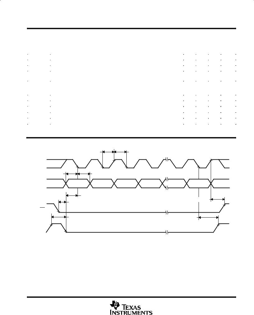
tsu(CS±FS) |
Setup time, |
|
low before FS↓ |
10 |
ns |
|||
CS |
||||||||
tsu(FS±CK) |
Setup time, FS low before first negative SCLK edge |
8 |
ns |
|||||
tsu(C16±FS) |
Setup time, sixteenth negative edge after FS low on which bit D0 is sampled before rising |
10 |
ns |
|||||
edge of FS |
||||||||
|
|
|
||||||
|
|
|
|
|||||
|
Setup time, sixteenth positive SCLK edge (first positive after D0 is sampled) before |
|
rising |
|
|
|||
|
CS |
|
|
|||||
tsu(C16±CS) |
edge. If FS is used instead of the sixteenth positive edge to update the DAC, then the setup |
10 |
ns |
|||||
|
time is between the FS rising edge and CS rising edge. |
|
|
|||||
|
|
|
|
|||||
twH |
Pulse duration, SCLK high |
25 |
ns |
|||||
twL |
Pulse duration, SCLK low |
25 |
ns |
|||||
tsu(D) |
Setup time, data ready before SCLK falling edge |
8 |
ns |
|||||
th(D) |
Hold time, data held valid after SCLK falling edge |
5 |
ns |
|||||
twH(FS) |
Pulse duration, FS high |
20 |
ns |
|||||
PARAMETER MEASUREMENT INFORMATION
|
|
twL |
|
twH |
|
|
|
SCLK |
1 |
2 |
3 |
4 |
5 |
15 |
16 |
|
|||||||
|
tsu(D) |
th(D) |
|
|
|
|
|
DIN |
D15 |
D14 |
D13 |
D12 |
|
D1 |
D0 |
tsu(FS-CK)
tsu(C16-CS)
tsu(CS-FS)
CS
twH(FS) |
|
tsu(C16-FS) |
|
FS
Figure 1. Timing Diagram
POST OFFICE BOX 655303 •DALLAS, TEXAS 75265 |
7 |

TLV5614
2.7-V TO 5.5-V 12-BIT 3- S QUADRUPLE DIGITAL-TO-ANALOG CONVERTERS
WITH POWER DOWN
SLAS188 ± SEPTEMBER 1998
TYPICAL CHARACTERISTICS
VO ± Output ± V
LOAD REGULATION |
LOAD REGULATION |
0.2 |
VDD = 3 V, |
|
|
|
|
|
|
0.35 |
||
0.18 |
|
|
|
|
|
|
|
|||
Vref = 1 V, |
|
|
|
|
|
|
0.30 |
|||
0.16 |
VO = Full Scale |
|
|
|
|
|
||||
|
|
|
|
|
|
|
|
|
|
|
0.14 |
|
|
|
|
|
|
|
|
|
0.25 |
|
|
|
|
3 V Slow Mode, Sink |
|
V |
|
|||
0.12 |
|
|
|
|
± |
|
||||
|
|
|
|
|
|
|
|
0.20 |
||
|
|
|
|
|
|
|
|
Output± |
||
|
|
|
|
|
|
|
|
|
||
0.10 |
|
|
|
3 V Fast Mode, Sink |
|
|
||||
|
|
|
|
|
|
|||||
0.08 |
|
|
|
|
|
|
|
|
O |
0.15 |
|
|
|
|
|
|
|
|
|
||
|
|
|
|
|
|
|
|
|
|
|
0.06 |
|
|
|
|
|
|
|
|
V |
|
|
|
|
|
|
|
|
|
|
0.10 |
|
|
|
|
|
|
|
|
|
|
|
|
0.04 |
|
|
|
|
|
|
|
|
|
|
0.02 |
|
|
|
|
|
|
|
|
|
0.05 |
|
|
|
|
|
|
|
|
|
|
|
0 |
0 |
0.01 |
0.02 |
0.05 |
0.1 |
0.2 |
0.5 |
1 |
2 |
0 |
|
|
|||||||||
|
|
|
Load Current ± mA |
|
|
|
|
|||
VDD = 5 V, |
|
|
|
|
|
|
||
Vref = 2 V, |
|
|
|
|
|
|
||
VO = Full Scale |
|
|
|
|
|
|
||
|
|
|
5 V Slow Mode, Sink |
|
|
|||
|
|
|
5 V Fast Mode, Sink |
|
|
|||
0 |
0.02 |
0.04 |
0.1 |
0.2 |
0.4 |
1 |
2 |
4 |
Load Current ± mA
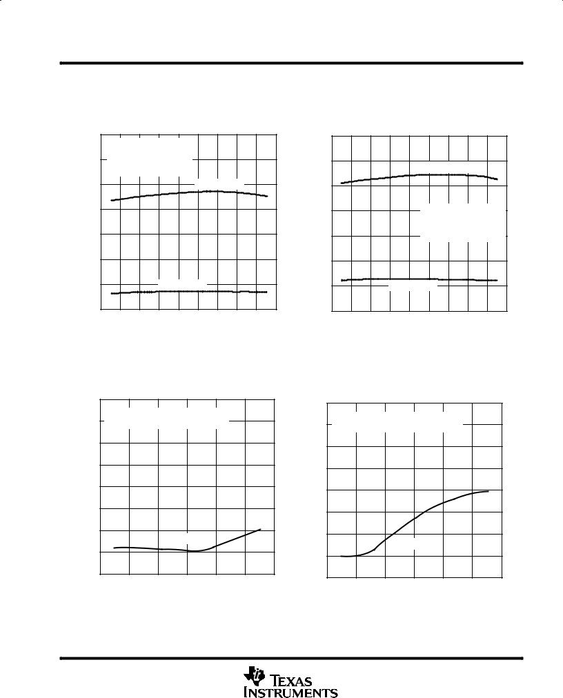
Figure 2 |
Figure 3 |
LOAD REGULATION |
LOAD REGULATION |
|
4.01 |
|
|
|
|
|
|
|
|
2.001 |
|
|
|
5 V Slow Mode, Source |
|
|
2.001 |
||||
|
4.005 |
|
|
|
|
|
|
|
|
2.000 |
± V |
|
|
|
|
|
|
|
|
± V |
2.000 |
4 |
|
|
|
|
|
|
|
1.999 |
||
± Output |
|
5 V Fast Mode, Source |
|
± Output |
||||||
|
|
|
|
|||||||
|
|
|
|
|
|
|
|
1.999 |
||
3.995 |
|
|
|
|
|
|
|
|
||
O |
|
|
|
|
|
|
|
O 1.998 |
||
V |
|
|
|
|
|
|
|
|
V |
|
|
|
|
|
|
|
|
|
|
|
1.998 |
|
3.99 |
|
|
|
|
|
VDD = 5 V, |
|
1.997 |
|
|
|
|
|
|
|
|
Vref = 2 V, |
|
1.997 |
|
|
|
|
|
|
|
|
VO = Full Scale |
|
||
|
3.985 |
0.02 |
0.04 |
0.1 |
0.2 |
0.4 |
1 |
2 |
4 |
1.996 |
|
0 |
|
||||||||
|
|
|
Load Current ± mA |
|
|
|
||||
3 V Slow Mode, Source |
3 V Fast Mode, Source |
VDD = 3 V, |
Vref = 1 V, |
VO = Full Scale |
0 |
0.01 |
0.02 0.05 |
0.1 |
0.2 |
0.5 |
1 |
2 |
Load Current ± mA
Figure 4 |
Figure 5 |
8 |
POST OFFICE BOX 655303 •DALLAS, TEXAS 75265 |
TLV5614 2.7-V TO 5.5-V 12-BIT 3- S QUADRUPLE DIGITAL-TO-ANALOG CONVERTERS
WITH POWER DOWN
SLAS188 ± SEPTEMBER 1998
TYPICAL CHARACTERISTICS
SUPPLY CURRENT |
SUPPLY CURRENT |
|
|
|
|
|
|
vs |
|
|
|
|
|
|
|
|
|
vs |
|
|
|
|
|
|
|
|
TEMPERATURE |
|
|
|
|
|
|
|
TEMPERATURE |
|
|
|
|||||
|
4 |
VDD = 3 V, |
|
|
|
|
|
|
|
4 |
|
|
|
|
|
|
|
|
||
|
|
|
|
|
|
|
|
|
|
|
|
|
|
|
|
|
|
|||
|
3.5 |
Vref = 1.024 V, |
|
|
|
|
|
|
|
3.5 |
|
|
|
|
|
|
|
|
||
|
VO Full Scale |
|
|
|
|
|
|
|
|
|
|
|
Fast Mode |
|
|
|||||
|
|
|
|
|
|
|
|
|
|
|
|
|
|
|
||||||
|
|
(Worst Case For IDD) |
|
|
|
|
|
|
|
|
|
|
|
|
||||||
mA |
|
|
|
|
|
mA |
|
|
|
|
|
|
|
|
|
|||||
3 |
|
|
|
|
|
Fast Mode |
|
|
3 |
|
|
|
|
|
|
|
|
|||
± |
|
|
|
|
|
|
|
|
|
|
± |
|
|
|
|
|
|
|
|
|
|
|
|
|
|
|
|
|
|
|
|
|
|
|
|
|
|
|
|
||
Current |
|
|
|
|
|
|
|
|
|
|
Current |
|
|
|
|
|
Vref = 1.024 V, |
|
|
|
Supply± |
2.5 |
|
|
|
|
|
|
|
|
|
Supply± |
2.5 |
|
|
|
|
VDD = 5 V, |
|
|
|
2 |
|
|
|
|
|
|
|
|
|
2 |
|
|
|
|
VO Full Scale |
|
|
|||
|
|
|
|
|
|
|
|
|
|
|
|
|
|
|
(Worst Case For IDD) |
|||||
DD |
1.5 |
|
|
|
|
|
|
|
|
|
DD |
1.5 |
|
|
|
|
|
|
|
|
I |
|
|
|
|
|
|
|
|
|
|
I |
|
|
|
|
|
|
|
|
|
|
1 |
|
|
|
Slow Mode |
|
|
|
|
1 |
|
|
Slow Mode |
|
|
|
||||
|
0.5 |
±55 |
±40 |
±25 |
0 |
25 |
40 |
70 |
85 |
125 |
|
0.5 |
|
|
|
|
|
|
85 |
125 |
|
|
|
±55 |
±40 |
±25 |
0 |
25 |
40 |
70 |
|||||||||||
|
|
|
|
T ± Temperature ± °C |
|
|
|
|
|
T ± Temperature ± °C |
|
|
||||||||
Figure 6 |
Figure 7 |
|
|
TOTAL HARMONIC DISTORTION |
|
|
|
TOTAL HARMONIC DISTORTION |
|
||||||||
|
|
|
|
vs |
|
|
|
|
|
|
|||||
|
|
|
|
|
|
|
|
|
|
|
vs |
|
|
|
|
|
|
|
|
FREQUENCY |
|
|
|
|
|
|
|
|
|
||
|
|
|
|
|
|
|
|
|
FREQUENCY |
|
|
||||
|
0 |
|
|
|
|
|
|
|
|
|
|
|
|||
|
|
|
|
|
|
|
|
0 |
|
|
|
|
|
|
|
|
|
|
|
|
|
|
|
|
|
|
|
|
|
|
|
|
±10 |
Vref = 1 V dc + 1 V p/p Sinewave, |
|
|
|
|
Vref = 1 V dc + 1 V p/p Sinewave, |
|
|
||||||
HarmonicTotal±THD Distortion ± dB |
Output Full Scale |
|
|
|
HarmonicTotal±THD Distortion ± dB |
±10 |
Output Full Scale |
|
|
|
|||||
|
|
|
|
|
|
|
|
|
|
||||||
±70 |
|
|
|
|
|
|
|
|
|
|
|
|
|
||
|
±20 |
|
|
|
|
|
|
|
±20 |
|
|
|
|
|
|
|
±30 |
|
|
|
|
|
|
|
±30 |
|
|
|
|
|
|
|
±±40 |
|
|
|
|
|
|
|
±±40 |
|
|
|
|
|
|
|
|
|
|
|
|
|
|
|
|
|
|
|
|
|
|
|
±50 |
|
|
|
|
|
|
|
±50 |
|
|
|
|
|
|
|
|
|
|
|
|
|
|
|
|
|
|
|
|
|
|
|
±60 |
|
|
Fast Mode |
|
|
|
|
±60 |
|
|
|
|
|
|
|
|
|
|
|
|
|
|
|
|
|
|
|
|
||
|
|
|
|
|
|
|
|
|
|
|
Slow Mode |
|
|
|
|
|
|
|
|
|
|
|
|
|
|
|
|
|
|
|
|
|
|
|
|
|
|
|
|
|
±70 |
|
|
|
|
|
|
|
±80 |
|
|
|
30 |
50 |
100 |
|
±80 |
|
|
|
|
|
|
|
0 |
5 |
10 |
20 |
|
|
|
|
30 |
50 |
100 |
||||
|
|
0 |
5 |
10 |
20 |
||||||||||
|
|
|
f ± Frequency ± kHz |
|
|
|
|||||||||
|
|
|
|
|
|
|
|
f ± Frequency ± kHz |
|
|
|||||
|
|
|
|
|
|
|
|
|
|
|
|
|
|||
Figure 8 |
Figure 9 |
POST OFFICE BOX 655303 •DALLAS, TEXAS 75265 |
9 |
 Loading...