


Texas Instruments TLV2543IN, TLV2543IDWR, TLV2543IDW, TLV2543IDB, TLV2543EVM Datasheet
...TLV2543C, TLV2543I 12-BIT ANALOG-TO-DIGITAL CONVERTERS WITH SERIAL CONTROL AND 11 ANALOG INPUTS
SLAS096B ± MARCH 1995 ± REVISED OCTOBER 1995
D |
12-Bit-Resolution A/D Converter |
DB, DW, OR N PACKAGE |
|
D |
10-μs Conversion Time Over Operating |
||
(TOP VIEW) |
|||
|
Temperature Range |
||
|
|
D D D D D D D
D D D D
11 Analog Input Channels
3 Built-In Self-Test Modes
Inherent Sample and Hold Function
Linearity Error . . . ± 1 LSB Max
On-Chip System Clock
End-of-Conversion (EOC) Output
Unipolar or Bipolar Output Operation (Signed Binary With Respect to Half of the Applied Referenced Voltage)
Programmable MSB or LSB First
Programmable Power Down
Programmable Output Data Length
CMOS Technology
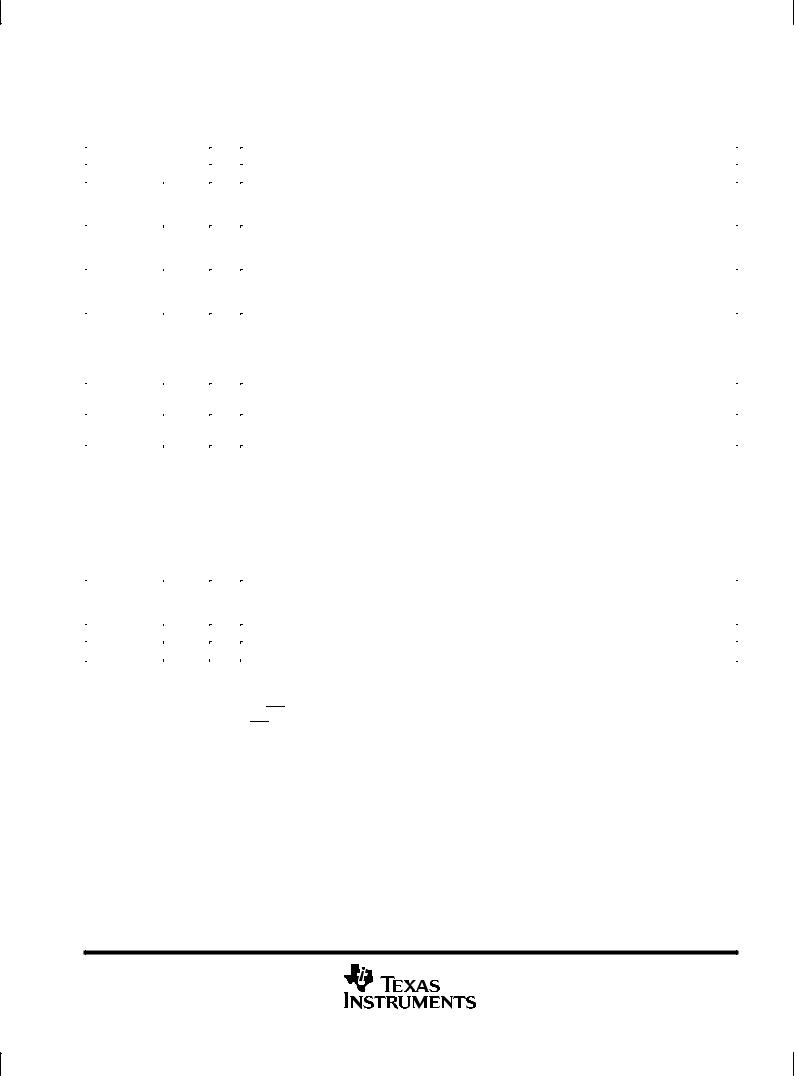
AIN0 |
|
1 |
20 |
|
|
VCC |
|
|
|
|
|||||
|
|
|
|
||||
AIN1 |
|
2 |
19 |
|
|
EOC |
|
AIN2 |
|
3 |
18 |
|
|
I/O CLOCK |
|
|
|
|
|||||
AIN3 |
|
4 |
17 |
|
|
DATA INPUT |
|
|
|
|
|||||
AIN4 |
|
5 |
16 |
|
|
DATA OUT |
|
|
|
|
|||||
AIN5 |
|
|
|
|
|
|
|
|
6 |
15 |
|
|
CS |
|
|
AIN6 |
|
7 |
14 |
|
|
REF+ |
|
|
|
|
|||||
AIN7 |
|
8 |
13 |
|
|
REF± |
|
|
|
|
|||||
AIN8 |
9 |
12 |
|
|
AIN10 |
||
|
|
||||||
GND |
10 |
11 |
|
|
AIN9 |
||
|
|
||||||
|
|
|
|
|
|
|
|
description
The TLV2543C and TLV2543I are 12-bit, switched-capacitor, successive-approximation, analog-to-digital converters (ADCs). Each device has three control inputs [chip select (CS), the input-output clock (I/O CLOCK), and the address input (DATA INPUT)] and is designed for communication with the serial port of a host processor or peripheral through a serial 3-state output. The device allows high-speed data transfers from the host.
In addition to the high-speed converter and versatile control capability, the device has an on-chip 14-channel multiplexer that can select any one of 11 inputs or any one of three internal self-test voltages. The sample-and-hold function is automatic. At the end of conversion, the end-of-conversion (EOC) output goes high to indicate that conversion is complete. The converter incorporated in the device features differential high-impedance reference inputs that facilitate ratiometric conversion, scaling, and isolation of analog circuitry from logic and supply noise. A switched-capacitor design allows low-error conversion over the full operating temperature range.
The TLV2543 is available in the DW, DB, and N packages. The TLV2543C is characterized for operation from 0°C to 70°C, and the TLV2543I is characterized for operation from ±40°C to 85°C.
AVAILABLE OPTIONS
|
|
PACKAGE |
|
|
|
|
|
TA |
SMALL OUTLINE |
PLASTIC DIP |
|
|
DW ² |
DB² |
N |
0°C to 70°C |
TLV2543CDW |
TLV2543CDB |
TLV2543CN |
|
|
|
|
± 40°C to 85°C |
TLV2543IDW |
Ð |
TLV2543IN |
|
|
|
|
² Available in tape and reel and ordered as the TLV2543CDWR, TLV2543CDBLE, or TLV2543IDWR.
Please be aware that an important notice concerning availability, standard warranty, and use in critical applications of Texas Instruments semiconductor products and disclaimers thereto appears at the end of this data sheet.
PRODUCTION DATA information is current as of publication date. Products conform to specifications per the terms of Texas Instruments standard warranty. Production processing does not necessarily include testing of all parameters.
Copyright 1995, Texas Instruments Incorporated
POST OFFICE BOX 655303 •DALLAS, TEXAS 75265 |
1 |

TLV2543C, TLV2543I |
|
|
|
|
|
|
||
12-BIT ANALOG-TO-DIGITAL CONVERTERS |
|
|
|
|
|
|||
WITH SERIAL CONTROL AND 11 ANALOG INPUTS |
|
|
|
|
||||
SLAS096B ± MARCH 1995 ± REVISED OCTOBER 1995 |
|
|
|
|
|
|||
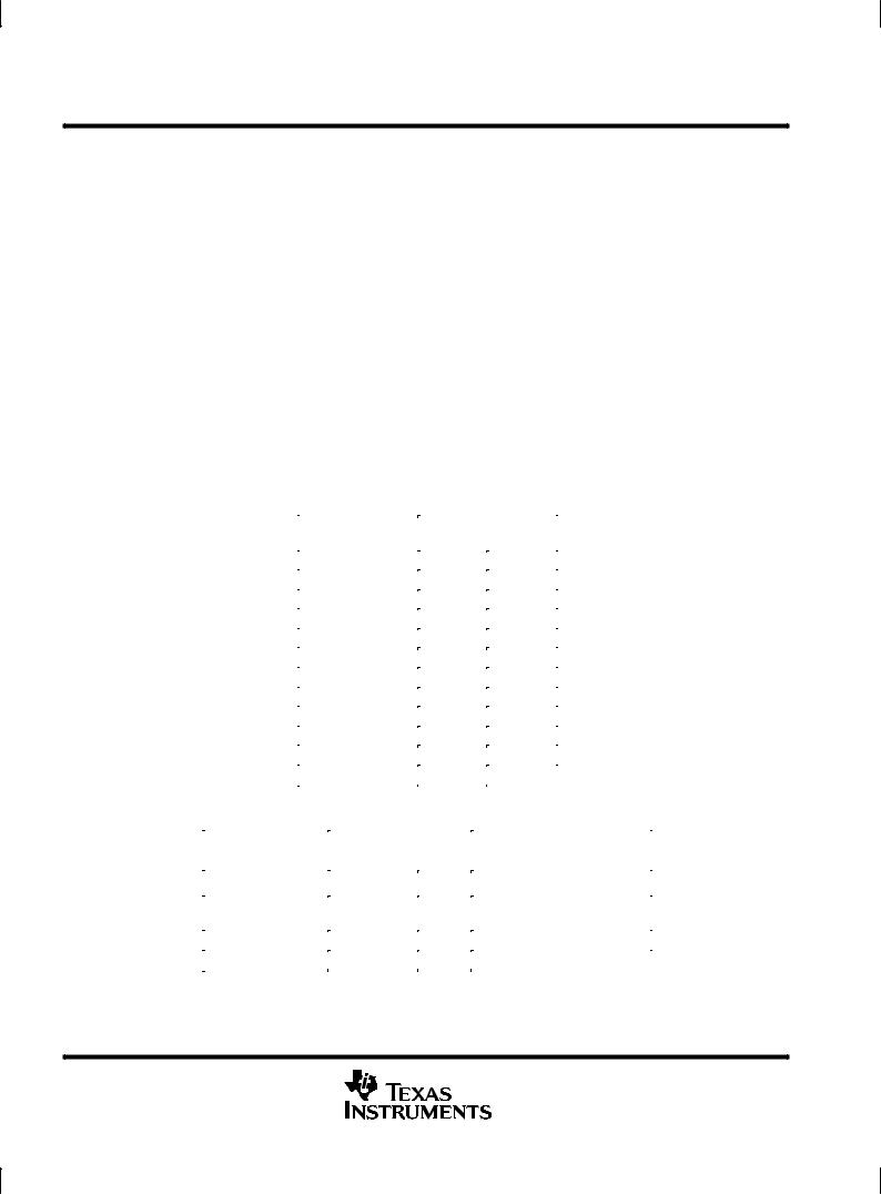
functional block diagram |
|
|
|
|
|
|
||
|
|
|
|
REF + |
REF ± |
|
|
|
|
|
|
|
14 |
13 |
|
|
|
AIN0 |
1 |
|
Sample and |
12-Bit |
|
|
|
|
|
Analog-to-Digital |
|
|
|
||||
AIN1 |
2 |
|
Hold |
Converter |
|
|
|
|
AIN2 |
3 |
|
|
(switched capacitors) |
|
|
|
|
AIN3 |
4 |
|
|
|
|
|
|
|
AIN4 |
5 |
14-Channel |
|
|
|
|
|
|
AIN5 |
6 |
|
12 |
|
|
|
|
|
AIN6 |
7 |
Analog |
|
|
|
|
|
|
Multiplexer |
|
|
|
|
|
|
||
AIN7 |
8 |
|
|
|
|
|
|
|
|
|
Output |
12 |
12-to-1 Data |
|
|
||
AIN8 |
9 |
|
|
16 |
DATA |
|||
|
|
Data |
|
Selector and |
||||
AIN9 |
11 |
|
|
|
|
OUT |
||
4 |
|
Register |
Driver |
|
||||
12 |
Input Address |
|
|
|||||
AIN10 |
|
|
|
|
|
|
||
|
|
|
Register |
|
|
|
|
|
|
|
|
|
|
|
4 |
|
|
|
3 |
|
|
|
|
|
|
|
|
|
Self-Test |
|
Control Logic |
|
|
|
|
|
|
|
and I/O |
|
|
|
|
|
|
|
Reference |
|
Counters |
|
|
|
|
DATA |
17 |
|
|
|
|
|
19 |
EOC |
|
|
|
|
|
|
|
||
INPUT |
|
|
|
|
|
|
|
|
I/O CLOCK |
18 |
|
|
|
|
|
|
|
15 |
|
|
|
|
|
|
|
|
CS |
|
|
|
|
|
|
|
|
|
|
|
|
|
|
|
|
|
2 |
POST OFFICE BOX 655303 •DALLAS, TEXAS 75265 |
|
|
|
|
|
|
|
|
|
TLV2543C, TLV2543I |
|
|
|
|
|
|
|
12-BIT ANALOG-TO-DIGITAL CONVERTERS |
||||
|
|
|
|
|
WITH SERIAL CONTROL AND 11 ANALOG INPUTS |
|||||
|
|
|
|
|
|
|
|
SLAS096B ± MARCH 1995 ± REVISED OCTOBER 1995 |
||
|
|
|
|
|
|
|
|
|
|
|
|
|
|
|
|
Terminal Functions |
|||||
|
|
|
|
|
|
|
|
|
|
|
|
|
TERMINAL |
I/O |
|
|
DESCRIPTION |
|
|||
|
|
NAME |
NO. |
|
|
|
||||
|
|
|
|
|
|
|
|
|
||
|
|
|
|
|
|
|
|
|
|
|
|
AIN0 ± AIN10 |
1 ± 9, |
I |
Analog input. These 11 analog-signal inputs are internally multiplexed. The driving source impedance should |
|
|||||
|
|
|
11, 12 |
|
be less than or equal to 50 Ω for 4.1-MHz I/O CLOCK operation and capable of slewing the analog input |
|
||||
|
|
|
|
|
voltage into a capacitance of 60 pF. |
|
||||
|
|
|
|
|
|
|
|
|
|
|
|
|
|
15 |
I |
Chip select. A high-to-low transition on |
|
resets the internal counters and controls and enables DATA OUT, |
|
||
|
CS |
|
CS |
|
||||||
|
|
|
|
|
DATA INPUT, and I/O CLOCK. A low-to-high transition disables DATA INPUT and I/O CLOCK within a setup |
|
||||
|
|
|
|
|
time. |
|
||||
|
|
|
|
|
|
|
|
|||
|
DATA INPUT |
17 |
I |
Serial-data input. A 4-bit serial address selects the desired analog input or test voltage to be converted. The |
|
|||||
|
|
|
|
|
serial data is presented with the MSB first and is shifted in on the first four rising edges of I/O CLOCK. After |
|
||||
|
|
|
|
|
the four address bits are read into the address register, I/O CLOCK clocks the remaining bits in order. |
|
||||
|
|
|
|
|
|
|
|
|||
|
DATA OUT |
16 |
O |
Serial data output. This is the 3-state serial output for the A/D conversion result. DATA OUT is in the |
|
|||||
|
|
|
|
|
high-impedance state when CS is high and active when |
CS |
is low. With a valid CS, DATA OUT is removed |
|
||
|
|
|
|
|
from the high-impedance state and is driven to the logic level corresponding to the MSB/LSB value of the |
|
||||
|
|
|
|
|
previous conversion result. The next falling edge of I/O CLOCK drives DATA OUT to the logic level |
|
||||
|
|
|
|
|
corresponding to the next MSB / LSB, and the remaining bits are shifted out in order. |
|
||||
|
|
|
|
|
|
|||||
|
EOC |
19 |
O |
End of conversion. EOC goes from a high to a low logic level after the falling edge of the last I/O CLOCK and |
|
|||||
|
|
|
|
|
remains low until the conversion is complete and data are ready for transfer. |
|
||||
|
|
|
|
|
|
|||||
|
GND |
10 |
|
Ground. This is the ground return terminal for the internal circuitry. Unless otherwise noted, all voltage |
|
|||||
|
|
|
|
|
measurements are with respect to GND. |
|
||||
|
|
|
|
|
|
|||||
|
I/O CLOCK |
18 |
I |
Input/output clock. I/O CLOCK receives the serial input and performs the following four functions: |
|
|||||
|
|
|
|
|
1. It clocks the eight input data bits into the input data register on the first eight rising edges of I/O CLOCK |
|
||||
|
|
|
|
|
with the multiplexer address available after the fourth rising edge. |
|
||||
|
|
|
|
|
2. On the fourth falling edge of I/O CLOCK, the analog input voltage on the selected multiplexer input |
|
||||
|
|
|
|
|
begins charging the capacitor array and continues to do so until the last falling edge of I/O |
|
||||
|
|
|
|
|
CLOCK. |
|
||||
|
|
|
|
|
3. It shifts the 11 remaining bits of the previous conversion data out on DATA OUT. Data changes on |
|
||||
|
|
|
|
|
the falling edge of I/O CLOCK. |
|
||||
|
|
|
|
|
4. It transfers control of the conversion to the internal state controller on the falling edge of the last |
|
||||
|
|
|
|
|
I/O CLOCK. |
|
||||
|
|
|
|
|
|
|||||
|
REF + |
14 |
I |
Reference+. The upper reference voltage value (nominally VCC) is applied to REF+. The maximum input |
|
|||||
|
|
|
|
|
voltage range is determined by the difference between the voltage applied to this terminal and the voltage |
|
||||
|
|
|
|
|
applied to the REF ± terminal. |
|
||||
|
|
|
|
|
|
|||||
|
REF ± |
13 |
I |
Reference±. The lower reference voltage value (nominally ground) is applied to REF ±. |
|
|||||
|
|
|
|
|
|
|||||
|
VCC |
20 |
|
Positive supply voltage. |
|
|||||
detailed description
Initially, with chip select (CS) high, I/O CLOCK and DATA INPUT are disabled and DATA OUT is in the high-impedance state. CS, going low, begins the conversion sequence by enabling I/O CLOCK and DATA INPUT and removes DATA OUT from the high-impedance state.
The input data is an 8-bit data stream consisting of a 4-bit analog channel address (D7±D4), a 2-bit data length select (D3±D2), an output MSB or LSB first bit (D1), and a unipolar or bipolar output select bit (D0) that are applied to DATA INPUT. The I/O CLOCK sequence applied to the I/O CLOCK terminal transfers this data to the input data register.
During this transfer, the I/O CLOCK sequence also shifts the previous conversion result from the output data register to DATA OUT. I/O CLOCK receives the input sequence of 8, 12, or 16 clocks long depending on the data-length selection in the input data register. Sampling of the analog input begins on the fourth falling edge of the input I/O CLOCK sequence and is held after the last falling edge of the I/O CLOCK sequence. The last falling edge of the I/O CLOCK sequence also takes EOC low and begins the conversion.
POST OFFICE BOX 655303 •DALLAS, TEXAS 75265 |
3 |

TLV2543C, TLV2543I
12-BIT ANALOG-TO-DIGITAL CONVERTERS
WITH SERIAL CONTROL AND 11 ANALOG INPUTS
SLAS096B ± MARCH 1995 ± REVISED OCTOBER 1995
converter operation
The operation of the converter is organized as a succession of two distinct cycles: 1) the I/O cycle, and 2) the actual conversion cycle. The I/O cycle is defined by the externally provided I/O CLOCK and lasts 8, 12, or 16 clock periods depending on the selected output data length.
1.I/O cycle
During the I/O cycle, two operations take place simultaneously.
a.An 8-bit data stream consisting of address and control information is provided to DATA INPUT. This data is shifted into the device on the rising edge of the first eight I/O CLOCKs. DATA INPUT is ignored after the first eight clocks during 12or 16-clock I/O transfers.
b.The data output with a length of 8, 12, or 16 bits is provided serially on DATA OUT. When CS is held low, the first output data bit occurs on the rising edge of EOC. When CS is negated between conversions, the first output data bit occurs on the falling edge of CS. This data is the result of the previous conversion period, and after the first output data bit each succeeding bit is clocked out on the falling edge of each succeeding I/O CLOCK.
2.Conversion cycle
The conversion cycle is transparent to the user, and it is controlled by an internal clock synchronized to the I/O CLOCK. During the conversion period, the device performs a successive-approximation conversion on the analog input voltage. The EOC output goes low at the start of the conversion cycle and goes high when conversion is complete and the output data register is latched. A conversion cycle is started only after the I/O cycle is completed, which minimizes the influence of external digital noise on the accuracy of the conversion.
power up and initialization
After power up, CS must be taken from high to low to begin an I/O cycle. EOC is initially high, and the input data register is set to all zeros. The contents of the output data register are random, and the first conversion result should be ignored. To initialize during operation, CS is taken high and returned low to begin the next I/O cycle. The first conversion after the device has returned from the power-down state may not read accurately due to internal device settling.
operational terminology
Previous (N ± 1) conversion cycle |
The conversion cycle prior to the current I/O cycle. |
|
|
Current (N) I/O cycle |
The entire I/O CLOCK sequence that transfers address and control data into the data register and clocks |
|
the digital result from the previous conversion cycle from DATA OUT. The last falling edge of the clock in |
|
the I/O CLOCK sequence signifies the end of the current I/O cycle. |
|
|
Current (N) conversion cycle |
Immediately after the current I/O cycle, the current conversion cycle starts. When the current conversion |
|
cycle is complete, the current conversion result is loaded into the output register. |
|
|
Current (N) conversion result |
The result of the current conversion cycle that is serially shifted out during the next I/O cycle. |
|
|
Next (N + 1) I/O cycle |
The I/O cycle after the current conversion cycle. |
Example: In the 12-bit mode, the result of the current conversion cycle is a 12-bit serial-data stream clocked out during the next I/O cycle. The current I/O cycle must be exactly 12 bits long to maintain synchronization, even when this corrupts the output data from the previous conversion. The current conversion begins immediately after the twelfth falling edge of the current I/O cycle.
data input
The data input is internally connected to an 8-bit serial-input address and control register. The register defines the operation of the converter and the output data length. The host provides the data word with the MSB first. Each data bit is clocked in on the rising edge of the I/O CLOCK sequence (see Table 1 for the data register format).
4 |
POST OFFICE BOX 655303 •DALLAS, TEXAS 75265 |

TLV2543C, TLV2543I 12-BIT ANALOG-TO-DIGITAL CONVERTERS WITH SERIAL CONTROL AND 11 ANALOG INPUTS
SLAS096B ± MARCH 1995 ± REVISED OCTOBER 1995
data input (continued)
Table 1. Input-Register Format
|
|
|
|
|
|
|
|
|
|
|
|
|
|
|
INPUT DATA BYTE |
|
|
|
|
|
|||
|
|
|
|
|
|
|
|
|
|
|
|
|
|
|
|
|
|
|
|
|
|
|
|
FUNCTION SELECT |
|
|
|
ADDRESS BITS |
|
|
L1 |
L0 |
|
LSBF |
|
BIP |
|||||||||||
|
|
|
|
|
|
|
|
|
|
|
|
|
|||||||||||
|
|
D7 |
D6 |
D5 |
D4 |
|
D3 |
D2 |
|
D1 |
|
D0 |
|||||||||||
|
|
|
|
|
|
|
|
|
|
|
|
|
|
|
|
||||||||
|
|
|
|
|
|
|
|
|
|
|
|
|
(MSB) |
|
|
|
|
|
|
|
|
|
(LSB) |
|
|
|
|
|
|
|
|
|
|
|
|
|
|
||||||||||
Select input channel |
|
|
|
|
|
|
|
|
|
|
|
|
|
||||||||||
AIN0 |
|
|
|
|
|
|
|
|
|
|
0 |
0 |
0 |
0 |
|
|
|
|
|
|
|
||
|
|
|
|
|
|
|
|
|
|
|
|
|
|
|
|
||||||||
AIN1 |
|
|
|
|
|
|
|
|
|
|
0 |
0 |
0 |
1 |
|
|
|
|
|
|
|
||
|
|
|
|
|
|
|
|
|
|
|
|
|
|
|
|
||||||||
AIN2 |
|
|
|
|
|
|
|
|
|
|
0 |
0 |
1 |
0 |
|
|
|
|
|
|
|
||
|
|
|
|
|
|
|
|
|
|
|
|
|
|
|
|
||||||||
AIN3 |
|
|
|
|
|
|
|
|
|
|
0 |
0 |
1 |
1 |
|
|
|
|
|
|
|
||
|
|
|
|
|
|
|
|
|
|
|
|
|
|
|
|
||||||||
AIN4 |
|
|
|
|
|
|
|
|
|
|
0 |
1 |
0 |
0 |
|
|
|
|
|
|
|
||
|
|
|
|
|
|
|
|
|
|
|
|
|
|
|
|
||||||||
AIN5 |
|
|
|
|
|
|
|
|
|
|
0 |
1 |
0 |
1 |
|
|
|
|
|
|
|
||
|
|
|
|
|
|
|
|
|
|
|
|
|
|
|
|
||||||||
AIN6 |
|
|
|
|
|
|
|
|
|
|
0 |
1 |
1 |
0 |
|
|
|
|
|
|
|
||
|
|
|
|
|
|
|
|
|
|
|
|
|
|
|
|
||||||||
AIN7 |
|
|
|
|
|
|
|
|
|
|
0 |
1 |
1 |
1 |
|
|
|
|
|
|
|
||
|
|
|
|
|
|
|
|
|
|
|
|
|
|
|
|
||||||||
AIN8 |
|
|
|
|
|
|
|
|
|
|
1 |
0 |
0 |
0 |
|
|
|
|
|
|
|
||
|
|
|
|
|
|
|
|
|
|
|
|
|
|
|
|
||||||||
AIN9 |
|
|
|
|
|
|
|
|
|
|
1 |
0 |
0 |
1 |
|
|
|
|
|
|
|
||
|
|
|
|
|
|
|
|
|
|
|
|
|
|
|
|
||||||||
AIN10 |
|
|
|
|
|
|
|
|
|
|
1 |
0 |
1 |
0 |
|
|
|
|
|
|
|
||
|
|
|
|
|
|
|
|
|
|
|
|
|
|
|
|
||||||||
Select test voltage |
|
|
|
|
|
|
|
|
|
|
|
|
|
||||||||||
(Vref + ± Vref ±)/2 |
|
|
|
|
1 |
0 |
1 |
1 |
|
|
|
|
|
|
|
||||||||
|
|
|
|
|
|
|
|
|
|
||||||||||||||
Vref ± |
|
|
|
|
|
|
|
|
1 |
1 |
0 |
0 |
|
|
|
|
|
|
|
||||
|
|
|
|
|
|
|
|
|
|
|
|
|
|
||||||||||
Vref + |
|
|
|
|
|
|
|
|
1 |
1 |
0 |
1 |
|
|
|
|
|
|
|
||||
|
|
|
|
|
|
|
|
|
|
|
|
|
|
||||||||||
Software power down |
|
|
|
|
1 |
1 |
1 |
0 |
|
|
|
|
|
|
|
||||||||
|
|
|
|
|
|
|
|
|
|
||||||||||||||
Output data length |
|
|
|
|
|
|
|
|
|
|
|
|
|
||||||||||
8 bits |
|
|
|
|
|
|
|
|
|
|
|
|
0 |
1 |
|
|
|
|
|||||
|
|
|
|
|
|
|
|
|
|
|
|
|
|
|
|||||||||
12 bits |
|
|
|
|
|
|
|
|
|
|
|
X |
0 |
|
|
|
|
||||||
|
|
|
|
|
|
|
|
|
|
|
|
|
|
||||||||||
16 bits |
|
|
|
|
|
|
|
|
|
|
|
1 |
1 |
|
|
|
|
||||||
|
|
|
|
|
|
|
|
|
|
|
|
|
|
||||||||||
Output data format |
|
|
|
|
|
|
|
|
|
|
|
|
|
||||||||||
MSB first |
|
|
|
|
|
|
|
|
|
|
|
|
0 |
|
|
||||||||
|
|
|
|
|
|
|
|
|
|
|
|
|
|||||||||||
LSB first |
|
|
|
|
|
|
|
|
|
|
|
|
1 |
|
|
||||||||
|
|
|
|
|
|
|
|
|
|
|
|
|
|||||||||||
Unipolar (binary) |
|
|
|
|
|
|
|
|
|
|
|
|
|
|
|
|
|
0 |
|||||
|
|
|
|
|
|
|
|
|
|
|
|
|
|||||||||||
Bipolar (BIP, 2s complement) |
|
|
|
|
|
|
|
|
|
|
|
|
|
1 |
|||||||||
|
|
|
|
|
|
|
|
|
|
|
|
||||||||||||
|
|
|
|
|
|
|
|
|
|
|
|
|
|
|
|
|
|
|
|
|
|
|
|
data input address bits
The four MSBs (D7 ± D4) of the data register address one of the 11 input channels, a reference-test voltage, or the power-down mode. The address bits affect the current conversion, which is the conversion that immediately follows the current I/O cycle. The reference voltage is nominally equal to Vref+ ± Vref ±.
data output length
The next two bits (D3 and D2) of the data register select the output data length. The data-length selection is valid for the current I/O cycle (the cycle in which the data is read). The data-length selection, which is valid for the current I/O cycle, allows device start-up without losing I/O synchronization. A data length of 8, 12, or 16 bits can be selected. Since the converter has 12-bit resolution, a data length of 12 bits is suggested.
With D3 and D2 set to 00 or 10, the device is in the 12-bit data-length mode and the result of the current conversion is output as a 12-bit serial-data stream during the next I/O cycle. The current I/O cycle must be exactly 12 bits long for proper synchronization, even when this means corrupting the output data from a previous conversion. The current conversion is started immediately after the twelfth falling edge of the current I/O cycle.
With bits D3 and D2 set to 11, the 16-bit data-length mode is selected, which allows convenient communication with 16-bit serial interfaces. In the 16-bit mode, the result of the current conversion is output as a 16-bit serial-data stream during the next I/O cycle with the four LSBs always set to 0 (pad bits). The current I/O cycle must be exactly 16 bits long to maintain synchronization even when this means corrupting the output data from the previous conversion. The current conversion is started immediately after the sixteenth falling edge of the current I/O cycle.
POST OFFICE BOX 655303 •DALLAS, TEXAS 75265 |
5 |

TLV2543C, TLV2543I
12-BIT ANALOG-TO-DIGITAL CONVERTERS
WITH SERIAL CONTROL AND 11 ANALOG INPUTS
SLAS096B ± MARCH 1995 ± REVISED OCTOBER 1995
data output length (continued)
With bits D3 and D2 set to 01, the 8-bit data-length mode is selected, which allows fast communication with 8-bit serial interfaces. In the 8-bit mode, the result of the current conversion is output as an 8-bit serial-data stream during the next I/O cycle. The current I/O cycle must be exactly 8 bits long to maintain synchronization, even when this means corrupting the output data from the previous conversion. The four LSBs of the conversion result are truncated and discarded. The current conversion is immediately started after the eighth falling edge of the current I/O cycle.
Since D3 and D2 take effect on the current I/O cycle when the data length is programmed, there can be a conflict with the previous cycle when the data-word length is changed from one cycle to the next. This may occur when the data format is selected to be least significant bit first, since at the time the data length change becomes effective (six rising edges of I/O CLOCK), the previous conversion result has already started shifting out.
In actual operation, when different data lengths are required within an application and the data length is changed between two conversions, no more than one conversion result can be corrupted and only when it is shifted out in LSB first format.
sampling period
During the sampling period, one of the analog inputs is internally connected to the capacitor array of the converter to store the analog input signal. The converter starts sampling the selected input immediately after the four address bits have been clocked into the input data register. Sampling starts on the fourth falling edge of I/O CLOCK. The converter remains in the sampling mode until the eighth, twelfth, or sixteenth falling edge of the I/O CLOCK depending on the data-length selection. After the EOC delay time from the last I/O CLOCK falling edge, the EOC output goes low indicating that the sampling period is over and the conversion period has begun. After EOC goes low, the analog input can be changed without affecting the conversion result. Since the delay from the falling edge of the last I/O CLOCK to EOC low is fixed, time-varying analog input signals can be digitized at a fixed rate without introducing systematic harmonic distortion or noise due to timing uncertainty.
After the 8-bit data stream has been clocked in, DATA INPUT should be held at a fixed digital level until EOC goes high (indicating that the conversion is complete) to maximize the sampling accuracy and minimize the influence of external digital noise.
data register, LSB first
D1 in the input data register (LSB first) controls the direction of the output binary data transfer. When D1 is set to 0, the conversion result shifts out MSB first. When set to 1, the data shifts out LSB first. Selection of MSB first or LSB first always affects the next I/O cycle and not the current I/O cycle. When changing from one data direction to another, the current I/O cycle is never disrupted.
data register, bipolar format
D0 in the input data register controls the binary data format used to represent the conversion result. When D0 is set to 0, the conversion result is represented as unipolar (unsigned binary) data. Nominally, the conversion result of an input voltage equal to Vref ± is a code of all zeros (000 . . . 0), the conversion result of an input voltage
equal to Vref + is a code of all ones (111 . . . 1), and the conversion result of (Vref + + Vref ±)/2 is a code of a one followed by zeros (100 . . . 0).
When D0 is set to 1, the conversion result is represented as bipolar data (signed binary). Nominally, conversion of an input voltage equal to Vref ± is a code of a 1 followed by zeros (100 . . . 0), conversion of an input voltage
equal to Vref + is a code of a 0 followed by all ones (011 . . . 1), and the conversion of (Vref + + Vref ±)/2 is a code of all zeros (000 . . . 0). The MSB is interpreted as the sign bit. The bipolar data format is related to the unipolar
format in that the MSBs are always each other's complement.
Selection of the unipolar or bipolar format always affects the current conversion cycle, and the result is output during the next I/O cycle. When changing between unipolar and bipolar formats, the data output during the current I/O cycle is not affected.
6 |
POST OFFICE BOX 655303 •DALLAS, TEXAS 75265 |

TLV2543C, TLV2543I 12-BIT ANALOG-TO-DIGITAL CONVERTERS WITH SERIAL CONTROL AND 11 ANALOG INPUTS
SLAS096B ± MARCH 1995 ± REVISED OCTOBER 1995
EOC output
The EOC signal indicates the beginning and the end of conversion. In the reset state, EOC is always high. During the sampling period (beginning after the fourth falling edge of the I/O CLOCK sequence), EOC remains high until the internal sampling switch of the converter is safely opened. The opening of the sampling switch occurs after the eighth, twelfth, or sixteenth I/O CLOCK falling edge, depending on the data-length selection in the input data register. After the EOC signal goes low, the analog input signal can be changed without affecting the conversion result.
The EOC signal goes high again after the conversion completes and the conversion result is latched into the output data register. The rising edge of EOC returns the converter to a reset state and a new I/O cycle begins. On the rising edge of EOC, the first bit of the current conversion result is on DATA OUT when CS is low. When CS is negated between conversions, the first bit of the current conversion result occurs at DATA OUT on the falling edge of CS.
data format and pad bits
D3 and D2 of the input data register determine the number of significant bits in the digital output that represent the conversion result. The LSB-first bit determines the direction of the data transfer while the BIP bit determines the arithmetic conversion. The numerical data is always justified toward the MSB in any output format.
The internal conversion result is always 12 bits long. When an 8-bit data transfer is selected, the four LSBs of the internal result are discarded to provide a faster one-byte transfer. When a 12-bit transfer is used, all bits are transferred. When a 16-bit transfer is used, four LSB pad bits are always appended to the internal conversion result. In the LSB-first mode, four leading zeros are output. In the MSB-first mode, the last four bits output are zeros.
When CS is held low continuously, the first data bit of the just completed conversion occurs on DATA OUT on the rising edge of EOC. When a new conversion is started after the last falling edge of I/O CLOCK, EOC goes low and the serial output is forced to a logic zero until EOC goes high again.
When CS is negated between conversions, the first data bit occurs on DATA OUT on the falling edge of CS. On each subsequent falling edge of I/O CLOCK after the first data bit appears, the data is changed to the next bit in the serial conversion result until the required number of bits has been output.
chip-select input (CS)
The chip-select input (CS) enables and disables the device. During normal operation, CS should be low. Although the use of CS is not necessary to synchronize a data transfer, it can be brought high between conversions to coordinate the data transfer of several devices sharing the same bus.
When CS is brought high, the serial-data output is immediately brought to the high-impedance state, releasing its output data line to other devices that may share it. After an internally generated debounce time, the I/O CLOCK is inhibited, thus preventing any further change in the internal state.
When CS is subsequently brought low again, the device is reset. CS must be held low for an internal debounce time before the reset operation takes effect. After CS is debounced low, I/O CLOCK must remain inactive (low) for a minimum time before a new I/O cycle can start.
CS can be used to interrupt any ongoing data transfer or any ongoing conversion. When CS is debounced low long enough before the end of the current conversion cycle, the previous conversion result is saved in the internal output buffer and then shifted out during the next I/O cycle.
POST OFFICE BOX 655303 •DALLAS, TEXAS 75265 |
7 |
TLV2543C, TLV2543I
12-BIT ANALOG-TO-DIGITAL CONVERTERS
WITH SERIAL CONTROL AND 11 ANALOG INPUTS
SLAS096B ± MARCH 1995 ± REVISED OCTOBER 1995
power-down features
When a binary address of 1110 is clocked into the input data register during the first four I/O CLOCK cycles, the power-down mode is selected. Power down is activated on the falling edge of the fourth I/O CLOCK pulse.
During power down, all internal circuitry is put in a low-current standby mode. No conversions are performed, and the internal output buffer keeps the previous conversion cycle data results, provided that all digital inputs are held above VCC ± 0.3 V or below 0.3 V. The I/O logic remains active so the current I/O cycle must be completed even when the power-down mode is selected. Upon power-on reset and before the first I/O cycle, the converter normally begins in the power-down mode. The device remains in the power-down mode until a valid (other than 1110) input address clocks in. Upon completion of that I/O cycle, a normal conversion is performed with the results being shifted out during the next I/O cycle.
analog input, test, and power-down mode
The 11 analog inputs, three internal voltages, and power-down mode are selected by the input multiplexer according to the input addresses shown in Tables 2, 3, and 4. The input multiplexer is a break-before-make type to reduce input-to-input noise rejection resulting from channel switching. Sampling of the analog input starts on the falling edge of the fourth I/O CLOCK and continues for the remaining I/O CLOCK pulses. The sample is held on the falling edge of the last I/O CLOCK pulse. The three internal test inputs are applied to the multiplexer, sampled, and converted in the same manner as the external analog inputs. The first conversion after the device has returned from the power-down state may not read accurately due to internal device settling.
Table 2. Analog-Channel-Select Address
ANALOG INPUT |
VALUE SHIFTED INTO |
||
DATA INPUT |
|||
SELECTED |
|||
|
|
||
BINARY |
HEX |
||
|
|||
|
|
|
|
AIN0 |
0000 |
0 |
|
|
|
|
|
AIN1 |
0001 |
1 |
|
|
|
|
|
AIN2 |
0010 |
2 |
|
|
|
|
|
AIN3 |
0011 |
3 |
|
|
|
|
|
AIN4 |
0100 |
4 |
|
|
|
|
|
AIN5 |
0101 |
5 |
|
|
|
|
|
AIN6 |
0110 |
6 |
|
|
|
|
|
AIN7 |
0111 |
7 |
|
|
|
|
|
AIN8 |
1000 |
8 |
|
|
|
|
|
AIN9 |
1001 |
9 |
|
|
|
|
|
AIN10 |
1010 |
A |
|
|
|
|
|
Table 3. Test-Mode-Select Address
|
INTERNAL |
VALUE SHIFTED INTO |
UNIPOLAR OUTPUT |
||
|
SELF-TEST |
DATA INPUT |
|||
|
VOLTAGE |
|
|
RESULT (HEX)³ |
|
|
SELECTED² |
BINARY |
HEX |
|
|
|
Vref + ± Vref ± |
|
1011 |
B |
200 |
2 |
|
||||
|
|
|
|
||
|
|
|
|
|
|
|
Vref ± |
1100 |
C |
000 |
|
|
Vref + |
1101 |
D |
3FF |
|
² Vref + is the voltage applied to REF +, and Vref ± is the voltage applied to REF ±.
³The output results shown are the ideal values and may vary with the reference stability and with internal offsets.
8 |
POST OFFICE BOX 655303 •DALLAS, TEXAS 75265 |
 Loading...