Texas Instruments TLV2217-33PWLE, TLV2217-33PWR, TLV2217-33MJB, TLV2217-33MFKB, TLV2217-33KTPR Datasheet

TLV2217-33
LOW-DROPOUT 3.3-V FIXED-VOLTAGE REGULATORS
SLVS067G ± MARCH 1992 ± REVISED JULY 1999
D |
Fixed 3.3-V Output |
|
|
|
PW PACKAGE |
|
|
|||||
D ±1% Maximum Output Voltage Tolerance at |
|
|
|
|
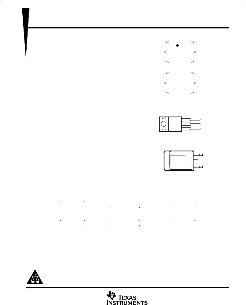
(TOP VIEW) |
|
|
|||||
|
|
|
|
|
|
|
|
|
|
|
||
|
TJ = 25°C |
|
|
|
|
|
1 |
20 |
|
|
|
|
|
|
|
|
|
|
|
|
|
|
|||
D |
500-mV Maximum Dropout Voltage at |
HEAT |
|
|
|
|
2 |
19 |
|
|
|
HEAT |
|
|
|
|
|||||||||
|
|
|
|
|
|
|||||||
|
500 mA |
SINK |
|
|
|
|
3 |
18 |
|
|
|
SINK |
|
|
|
|
|
|
|
||||||
D |
500-mA Dropout Current |
|
|
|
|
|
4 |
17 |
|
|
|
|
|
|
|
|
|
|
|
|
|
||||
D ±2% Absolute Output Voltage Variation |
GND |
|
|
5 |
16 |
|
|
GND |
||||
|
|
|
|
|||||||||
INPUT |
|
|
6 |
15 |
|
|
OUTPUT |
|||||
D |
Internal Overcurrent Limiting |
|
|
|
|
|||||||
|
|
|
|
|
7 |
14 |
|
|
|
|
||
|
|
|
|
|
|
|
|
|
||||
D Internal Thermal-Overload Protection |
|
|
|
|
|
|
|
|
|
|||
HEAT |
|
|
|
|
8 |
13 |
|
|
|
HEAT |
||
|
|
|
|
|
|
|
||||||
|
Internal Overvoltage Protection |
|
|
|
|
|
|
|
||||
D |
SINK |
|
|
|
|
9 |
12 |
|
|
|
SINK |
|
|
|
|
|
|
|
|
||||||
|
|
|
|
|||||||||
D Package Options Include Plastic Flange |
|
|
|
|
|
10 |
11 |
|
|
|
|
|
|
Mounted (KTP), Power (KC), and Thin |
|
|
|
|
|
|
|
|
|
|
|
|
HEAT SINK ± These terminals have an internal resistive connection |
|||||||||||
|
Shrink Small-Outline (PW) Packages |
|||||||||||
|
to ground and should be grounded or electrically isolated. |
|||||||||||
|
|
|||||||||||
description |
KC PACKAGE |
|
(TOP VIEW) |
The TLV2217-33 is a low-dropout 3.3-V fixedvoltage regulator. The regulator is capable of sourcing 500 mA of current with an input-output differential of 0.5 V, or less. The TLV2217-33 provides internal overcurrent limiting, thermaloverload protection, and overvoltage protection.
The 0.5-V dropout for the TLV2217-33 makes it ideal for battery applications in 3.3-V logic systems. For example, battery input voltage to the regulator can drop as low as 3.8 V, and the TLV2217-33 can continue to regulate the system. For higher voltage systems, the TLV2217-33 can be operated with a continuous input voltage of 12 V.
|
OUTPUT |
GND |
GND |
|
INPUT |
The GND terminal is in electrical contact with the mounting base.
|
KTP PACKAGE |
|
(TOP VIEW) |
|
OUTPUT |
GND |
GND |
|
INPUT |
The GND terminal is in electrical contact with the mounting base.
The TLV2217-33 regulators are characterized for virtual junction temperature operation from 0°C to 125°C .
AVAILABLE OPTIONS
|
|
PACKAGED DEVICES |
|
|
|
|
|
|
CHIP FORM |
TJ |
PLASTIC |
SURFACE |
PLASTIC |
|
POWER |
MOUNT |
FLANGE MOUNT |
(Y) |
|
|
(KC) |
(PW) |
(KTP) |
|
|
|
|
|
|
0°C to 125°C |
TLV2217-33KC |
TLV2217-33PW |
TLV2217-33KTP |
TLV2217-33Y |
The KTP and PW packages are available taped and reeled only. Add R suffix to device type (e.g., TLV2212-33PWR). Chip forms are tested at 25°C.
Please be aware that an important notice concerning availability, standard warranty, and use in critical applications of Texas Instruments semiconductor products and disclaimers thereto appears at the end of this data sheet.
PRODUCTION DATA information is current as of publication date. Products conform to specifications per the terms of Texas Instruments standard warranty. Production processing does not necessarily include testing of all parameters.
Copyright 1999, Texas Instruments Incorporated
POST OFFICE BOX 655303 •DALLAS, TEXAS 75265 |
1 |

TLV2217-33
LOW-DROPOUT 3.3-V FIXED-VOLTAGE REGULATORS
SLVS067G ± MARCH 1992 ± REVISED JULY 1999
absolute maximum ratings over operating virtual junction temperature range (unless otherwise noted)²
Continuous input voltage, VI . . . . . . . . . . . . . . . . . . . . . . . . . . . . . . . . . . . . . . . . . . . . . . . . . . . . . . . . |
. . . . . . . . . 16 V |
Package thermal impedance, θJA (see Notes 1 and 2): KC package . . . . . . . . . . . . . . . . . . . . . |
. . . . . . 22°C/W |
KTP package . . . . . . . . . . . . . . . . . . . |
. . . . . . 28°C/W |
PW package . . . . . . . . . . . . . . . . . . . . |
. . . . . . 83°C/W |
Storage temperature range, Tstg . . . . . . . . . . . . . . . . . . . . . . . . . . . . . . . . . . . . . . . . . . . . . . . . . . . |
±65°C to 150°C |
² Stresses beyond those listed under ªabsolute maximum ratingsº may cause permanent damage to the device. These are stress ratings only, and functional operation of the device at these or any other conditions beyond those indicated under ªrecommended operating conditionsº is not implied. Exposure to absolute-maximum-rated conditions for extended periods may affect device reliability.
NOTES: 1. Maximum power dissipation is a function of TJ(max), θJA, and TA. The maximum allowable power dissipation at any allowable ambient temperature is PD = (TJ(max) ± TA)/θJA. Operating at the absolute maximum TJ of 150°C can impact reliability. Due to variation in individual device electrical characteristics and thermal resistance, the built-in thermal overload protection may be activated at power levels slightly above or below the rated dissipation.
2.The package thermal impedance is calculated in accordance with JESD 51, except for through-hole packages, which use a trace length of zero.
recommended operating conditions
|
MIN |
MAX |
UNIT |
|
|
|
|
Input voltage, VI |
3.8 |
12 |
V |
Output current, IO |
0 |
500 |
mA |
Operating virtual junction temperature range, TJ |
0 |
125 |
°C |
electrical characteristics at VI = 4.5 V, IO = 500 mA, TJ = 25°C (unless otherwise noted)
PARAMETER |
|
TEST CONDITIONS³ |
TLV2217-33 |
UNIT |
|||
|
|
|
|
|
|||
|
MIN |
TYP |
MAX |
UNIT |
|||
|
|
|
|
||||
|
|
|
|
|
|
|
|
Output voltage |
IO = 20 mA to 500 mA, |
VI = 3.8 V to 5.5 V |
TJ = 25°C |
3.267 |
3.30 |
3.333 |
V |
TJ = 0°C to 125°C |
3.234 |
|
3.366 |
||||
|
|
|
|
|
|||
Input voltage regulation |
VI = 3.8 V to 5.5 V |
|
|
|
5 |
15 |
mV |
Ripple rejection |
f = 120 Hz, |
Vripple = 1 VPP |
|
±62 |
|
dB |
|
Output voltage regulation |
IO = 20 mA to 500 mA |
|
|
|
5 |
30 |
mV |
Output noise voltage |
f = 10 Hz to 100 kHz |
|
|
|
500 |
|
µV |
|
|
|
|
|
|
|
|
Dropout voltage |
IO = 250 mA |
|
|
|
|
400 |
mV |
IO = 500 mA |
|
|
|
|
500 |
||
|
|
|
|
|
|
||
Bias current |
IO = 0 |
|
|
|
2 |
5 |
mA |
IO = 500 mA |
|
|
|
19 |
49 |
||
|
|
|
|
|
|||
³Pulse-testing techniques are used to maintain the virtual junction temperature as close to the ambient temperature as possible. Thermal effects must be taken into account separately. All characteristics are measured with a 0.1-µF capacitor across the input and a 22-µF tantalum capacitor with equivalent series resistance of 1.5 Ω on the output.
2 |
POST OFFICE BOX 655303 •DALLAS, TEXAS 75265 |
 Loading...