


Texas Instruments TLV0831IDR, TLV0831CP, TLV0831ID, TLV0831CDR, TLV0831CD Datasheet
...TLV0831C, TLV0831I
TLV0832C, TLV0832I 3-VOLT 8-BIT ANALOG-TO-DIGITAL CONVERTERS WITH SERIAL CONTROL
SLAS148 ± SEPTEMBER 1996
D8-Bit Resolution
D2.7 V to 3.6 V VCC
DEasy Microprocessor Interface or Standalone Operation
DOperates Ratiometrically or With VCC Reference
DSingle Channel or Multiplexed Twin Channels With Single-Ended or Differential Input Options
TLV0831 . . . D OR P PACKAGE
(TOP VIEW)
|
|
|
|
|
|
|
CS |
1 |
8 |
VCC |
|
IN+ |
2 |
7 |
CLK |
||
IN± |
3 |
6 |
DO |
||
GND |
4 |
5 |
REF |
||
|
|
|
|
|
|
TLV0832 . . . D OR P PACKAGE
(TOP VIEW)
DInput Range 0 V to VCC With VCC Reference
|
Inputs and Outputs Are Compatible With |
|
|
|
|
|
|
|
|
D |
CS |
|
1 |
8 |
|
VCC /REF |
|||
|
TTL and MOS |
CH0 |
|
2 |
7 |
|
CLK |
||
D |
μ |
CH1 |
|
3 |
6 |
|
DO |
||
|
Conversion Time of 32 s at |
GND |
|
|
|
|
DI |
||
|
f(CLK) = 250 kHz |
|
4 |
5 |
|
||||
|
|
|
|||||||
DDesigned to Be Functionally Equivalent to the National Semiconductor ADC0831 and ADC0832 at 3 V Supply
DTotal Unadjusted Error . . . ± 1 LSB
description
These devices are 8-bit successive-approximation analog-to-digital converters. The TLV0831 has single input channels; the TLV0832 has multiplexed twin input channels. The serial output is configured to interface with standard shift registers or microprocessors.
The TLV0832 multiplexer is software configured for single-ended or differential inputs. The differential analog voltage input allows for common-mode rejection or offset of the analog zero input voltage value. In addition, the voltage reference input can be adjusted to allow encoding any smaller analog voltage span to the full 8 bits of resolution.
The operation of the TLV0831 and TLV0832 devices is very similar to the more complex TLV0834 and TLV0838 devices. Ratiometric conversion can be attained by setting the REF input equal to the maximum analog input signal value, which gives the highest possible conversion resolution. Typically, REF is set equal to VCC (done internally on the TLV0832).
The TLV0831C and TLV0832C are characterized for operation from 0°C to 70°C. The TLV0831I and TLV0832I are characterized for operation from ±40°C to 85°C.
AVAILABLE OPTIONS
|
|
PACKAGE |
|
|
TA |
|
|
||
SMALL OUTLINE |
PLASTIC DIP |
|||
|
|
(D) |
|
(P) |
|
|
|
|
|
0°C to 70°C |
TLV0831CD |
TLV0832CD |
TLV0831CP |
TLV0832CP |
|
|
|
|
|
± 40°C to 85°C |
TLV0831ID |
TLV0832ID |
TLV0831IP |
TLV0832IP |
|
|
|
|
|
Please be aware that an important notice concerning availability, standard warranty, and use in critical applications of Texas Instruments semiconductor products and disclaimers thereto appears at the end of this data sheet.
PRODUCTION DATA information is current as of publication date. Products conform to specifications per the terms of Texas Instruments standard warranty. Production processing does not necessarily include testing of all parameters.
Copyright 1996, Texas Instruments Incorporated
POST OFFICE BOX 655303 •DALLAS, TEXAS 75265 |
1 |
TLV0831C, TLV0831I
TLV0832C, TLV0832I
3-VOLT 8-BIT ANALOG-TO-DIGITAL CONVERTERS WITH SERIAL CONTROL
SLAS148 ± SEPTEMBER 1996
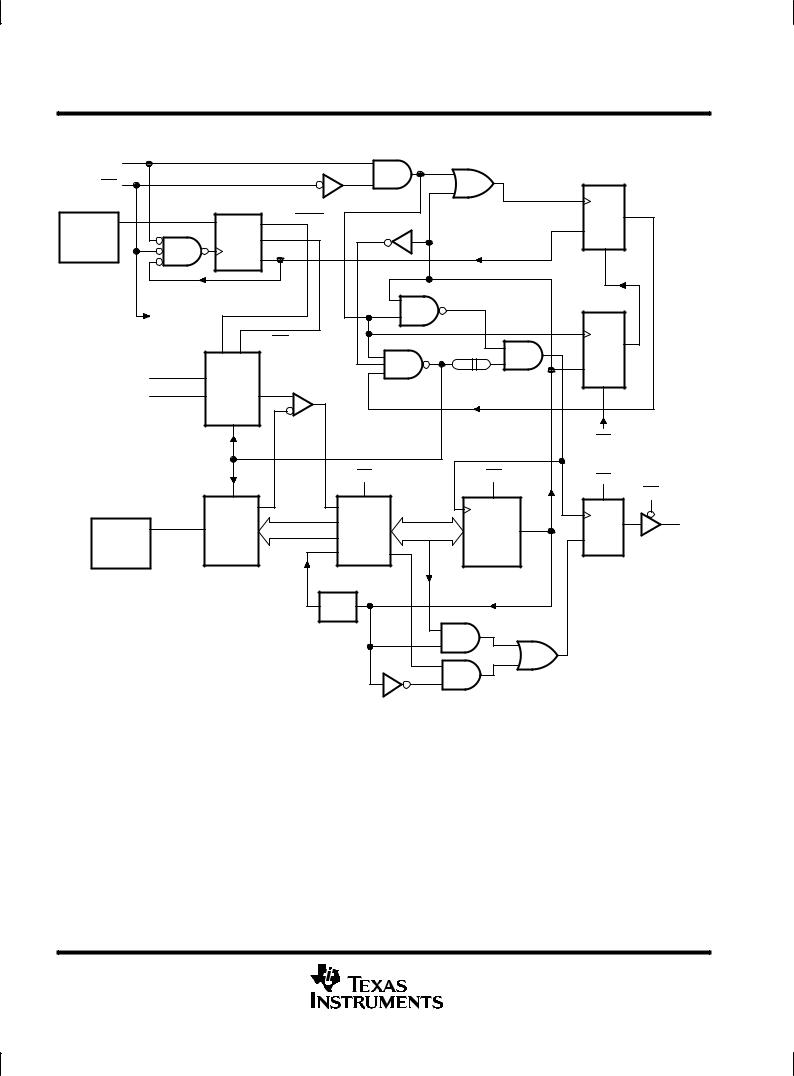
functional block diagram
CLK |
|
|
|
|
|
|
Start |
|
CS |
|
|
|
|
|
|
Flip-Flop |
|
|
|
|
|
|
|
|
|
|
|
Shift Register |
|
|
|
|
CLK |
|
|
DI |
D |
ODD/EVEN |
|
|
|
|
|
|
|
|
|
|
|
S |
|
||
(TLV0832 |
|
|
|
|
|
|
|
|
CLK |
Start |
|
|
|
|
R |
|
|
only) |
|
|
|
|
|
|
||
|
To Internal |
|
|
|
|
|
|
|
|
Circuits |
|
|
|
|
|
|
|
|
SGL/DIF |
|
|
|
|
CLK |
|
|
|
|
|
|
|
|
|
||
CH0/IN+ |
Analog |
|
|
|
|
|
S |
|
Comparator |
|
Time |
|
R |
|
|||
CH1/IN ± |
MUX |
|
|
|
Delay |
|
|
|
|
|
|
|
|
|
|
|
|
|
EN |
|
|
|
|
|
|
|
|
|
|
|
|
|
|
CS |
|
|
|
|
CS |
|
CS |
|
CS |
|
|
|
|
|
|
|
|
|
|
|
EN |
|
EN R |
|
CLK R |
|
|
CS |
|
|
|
|
R |
|
|||
REF |
Ladder |
|
SAR |
|
9-Bit |
EOC |
CLK |
DO |
Bits 0±7 |
Logic |
Bits 0±7 |
|
|||||
and |
|
D |
|
|||||
(TLV0831 |
|
and |
|
Shift |
|
|
||
Decoder |
|
|
|
|
||||
only) |
|
Latch |
Bit 1 |
Register |
|
|
|
|
|
|
|
|
|
||||
|
|
|
MSB |
LSB |
|
|
|
|
|
|
|
First |
First |
|
|
|
|
|
|
|
One |
|
|
|
|
|
|
|
|
Shot |
|
|
|
|
|
2 |
POST OFFICE BOX 655303 •DALLAS, TEXAS 75265 |

TLV0831C, TLV0831I
TLV0832C, TLV0832I 3-VOLT 8-BIT ANALOG-TO-DIGITAL CONVERTERS WITH SERIAL CONTROL
SLAS148 ± SEPTEMBER 1996
functional description
The TLV0831 and TLV0832 use a sample-data-comparator structure that converts differential analog inputs by a successive-approximation routine. The input voltage to be converted is applied to an input terminal and is compared to ground (single ended), or to an adjacent input (differential). The TLV0832 input terminals can be assigned a positive (+) or negative (±) polarity. The TLV0831 contains only one differential input channel with fixed polarity assignment; therefore it does not require addressing. The signal can be applied differentially, between IN+ and IN±, to the TLV0831 or can be applied to IN+ with IN± grounded as a single ended input. When the signal input applied to the assigned positive terminal is less than the signal on the negative terminal, the converter output is all zeros.
Channel selection and input configuration are under software control using a serial-data link from the controlling processor. A serial-communication format allows more functions to be included in a converter package with no increase in size. In addition, it eliminates the transmission of low-level analog signals by locating the converter at the analog sensor and communicating serially with the controlling processor. This process returns noise-free digital data to the processor.
A conversion is initiated by setting CS low, which enables all logic circuits. CS must be held low for the complete conversion process. A clock input is then received from the processor. An interval of one clock period is automatically inserted to allow the selected multiplexed channel to settle. DO comes out of the high-impedance state and provides a leading low for one clock period of multiplexer settling time. The SAR comparator compares successive outputs from the resistive ladder with the incoming analog signal. The comparator output indicates whether the analog input is greater than or less than the resistive-ladder output. As the conversion proceeds, conversion data is simultaneously output from DO, with the most significant bit (MSB) first. After eight clock periods, the conversion is complete. When CS goes high, all internal registers are cleared. At this time, the output circuits go to the high-impedance state. If another conversion is desired, CS must make a high-to-low transition followed by address information.
A TLV0832 input configuration is assigned during the multiplexer-addressing sequence. The multiplexer address shifts into the converter through the data input (DI) line. The multiplexer address selects the analog inputs to be enabled and determines whether the input is single ended or differential. When the input is differential, the polarity of the channel input is assigned. In addition to selecting the differential mode, the polarity may also be selected. Either channel of the channel pair may be designated as the negative or positive input.
On each low-to-high transition of the clock input, the data on DI is clocked into the multiplexer-address shift register. The first logic high on the input is the start bit. A 2-bit assignment word follows the start bit on the TLV0832. On each successive low-to-high transition of the clock input, the start bit and assignment word are shifted through the shift register. When the start bit is shifted into the start location of the multiplexer register, the input channel is selected and conversion starts. The TLV0832 DI terminal to the multiplexer shift register is disabled for the duration of the conversion.
The TLV0832 outputs the least-significant-bit (LSB) first data after the MSB-first data stream. The DI and DO terminals can be tied together and controlled by a bidirectional processor I/O bit received on a single wire. This is possible because DI is only examined during the multiplexer-addressing interval and DO is still in the high-impedance state.
POST OFFICE BOX 655303 •DALLAS, TEXAS 75265 |
3 |

TLV0831C, TLV0831I
TLV0832C, TLV0832I
3-VOLT 8-BIT ANALOG-TO-DIGITAL CONVERTERS WITH SERIAL CONTROL
SLAS148 ± SEPTEMBER 1996
sequence of operation
|
|
|
|
|
|
|
TLV0831 |
|
|
|
|
|
|
|
|
|
|
1 |
2 |
3 |
4 |
5 |
6 |
7 |
8 |
9 |
10 |
|
|
|
|
CLK |
|
|
|
|
|
|
|
|
|
|
|
|
|
|
|
|
tsu |
|
|
|
|
tconv |
|
|
|
|
|
|
|
|
|
|
|
|
|
|
|
|
|
|
|
|
|
|
|
|
|
CS |
|
|
|
|
|
|
|
|
|
|
|
|
|
|
|
|
MUX |
|
|
|
|
MSB-First Data |
|
|
|
|
|
|
|
||
|
|
|
|
|
|
|
|
|
|
|
|
|
|
|
|
Settling Time |
|
|
|
|
|
|
|
|
|
|
|
|
|
|
|
DO |
Hi-Z |
|
MSB |
|
|
|
|
|
|
|
LSB |
Hi-Z |
|
|
|
|
|
|
|
|
|
|
|
|
|
|
|
|
|||
|
|
|
|
7 |
6 |
5 |
4 |
3 |
2 |
1 |
|
0 |
|
|
|
|
|
|
|
|
|
|
|
|
|
|
|
|
|
|
|
|
|
|
|
|
|
|
TLV0832 |
|
|
|
|
|
|
|
|
1 |
2 |
3 |
4 |
5 |
6 |
|
10 |
11 |
12 |
13 |
14 |
18 |
19 |
20 |
21 |
CLK |
|
|
|
|
|
|
|
|
|
|
|
|
|
|
|
tsu |
|
|
|
tconv |
|
|
|
|
|
|
|
|
|
|
|
|
|
|
|
|
|
|
|
|
|
|
|
|
|
||
CS |
|
|
|
|
|
|
|
|
|
|
|
|
|
|
|
Start |
+Sign Bit |
|
|
|
|
|
|
|
|
|
|
|
|
|
|
SGL ODD |
|
|
|
|
|
|
|
|
|
|
|
|
|
||
Bit |
|
|
|
|
|
|
|
|
|
|
|
|
|
||
|
|
|
|
|
|
|
|
|
|
|
|
|
|
|
|
DI |
Don't Care |
|
(TLV0832 |
||
|
||
only) |
DIF EVEN |
|
|
MSB-First Data
LSB-First Data
MUX
Settling Time
Hi-Z
DO |
MSB |
|
|
|
LSB |
|
|
|
MSB |
|
7 |
6 |
2 |
1 |
0 |
1 |
2 |
6 |
7 |
TLV0832 MUX-ADDRESS CONTROL LOGIC TABLE
MUX ADDRESS |
|
CHANNEL NUMBER |
|||||
|
|
|
|
|
|
|
|
SGL/DIF |
|
ODD/EVEN |
|
CH0 |
CH1 |
||
L |
L |
|
+ |
± |
|||
L |
H |
|
± |
+ |
|||
H |
L |
|
+ |
+ |
|||
H |
H |
|
|
||||
|
|
|
|
|
|
|
|
H = high level, L = low level,
± or + = terminal polarity for the selected input channel
4 |
POST OFFICE BOX 655303 •DALLAS, TEXAS 75265 |
 Loading...