


Texas Instruments TLV1570IPW, TLV1570IPWR, TLV1570IDWR, TLV1570IDW, TLV1570CPWR Datasheet
...TLV1570 2.7 V TO 5.5 V 8-CHANNEL 10-BIT 1.25-MSPS SERIAL ANALOG-TO-DIGITAL CONVERTER
SLAS169A ± DECEMBER 1997± REVISED SEPTEMBER 1998
DFast Throughput Rate: 1.25 MSPS at 5 V,
625 KSPS at 3 V
DWide Analog Channel Input: 0 V to AVDD
DEight Analog Input Channels
DChannel Auto-Scan
DDifferential Nonlinearity Error: < ±1 LSB
DIntegral Nonlinearity Error: < ±1 LSB
DSignal-to-Noise and Distortion Ratio: 57 dB
DSingle 2.7-V to 5.5-V Supply Operation
DVery Low Power: 40 mW at 5.5 V,
8 mW at 2.7 V
DAuto-Power Down: 300 μA Max
DSoftware Power Down: 10 μA Max
DGlueless Serial Interface to TMS320 DSPs and (Q)SPI Compatible Microcontrollers
DProgrammable Internal Reference Voltage: 3.8-V Reference for 5-V Operation, 2.3-V Reference for 3-V Operation
description
applications
DMass Storage and Hard Disk Drive
DAutomotive
DDigital Servos
DProcess Control
DGeneral Purpose DSP
DImage Sensor Processing
DW OR PW PACKAGE
(TOP VIEW)
|
|
|
|
|
|
|
|
|
|
CH4 |
|
|
|
1 |
20 |
|
|
|
AIN |
CH3 |
|
|
|
2 |
19 |
|
|
|
MO |
|
|
|
|
||||||
CH2 |
|
|
3 |
18 |
|
|
|
CH5 |
|
|
|
|
|
||||||
CH1 |
|
|
4 |
17 |
|
|
|
CH6 |
|
|
|
|
|
||||||
CH0 |
|
|
|
5 |
16 |
|
|
|
CH7 |
|
|
|
|
||||||
DVDD |
|
|
|
6 |
15 |
|
|
|
AVDD |
|
|
|
|
||||||
|
|
|
|
||||||
DGND |
|
|
|
7 |
14 |
|
|
|
AGND |
FS |
|
|
|
8 |
13 |
|
|
|
REF |
|
|
|
|
||||||
SCLK |
|
|
|
9 |
12 |
|
|
|
CS |
|
|
|
|
||||||
SDIN |
|
|
|
10 |
11 |
|
|
|
SDOUT |
|
|
|
|
||||||
|
|
|
|
|
|
|
|
|
|
|
|
|
|
|
|
|
|
|
|
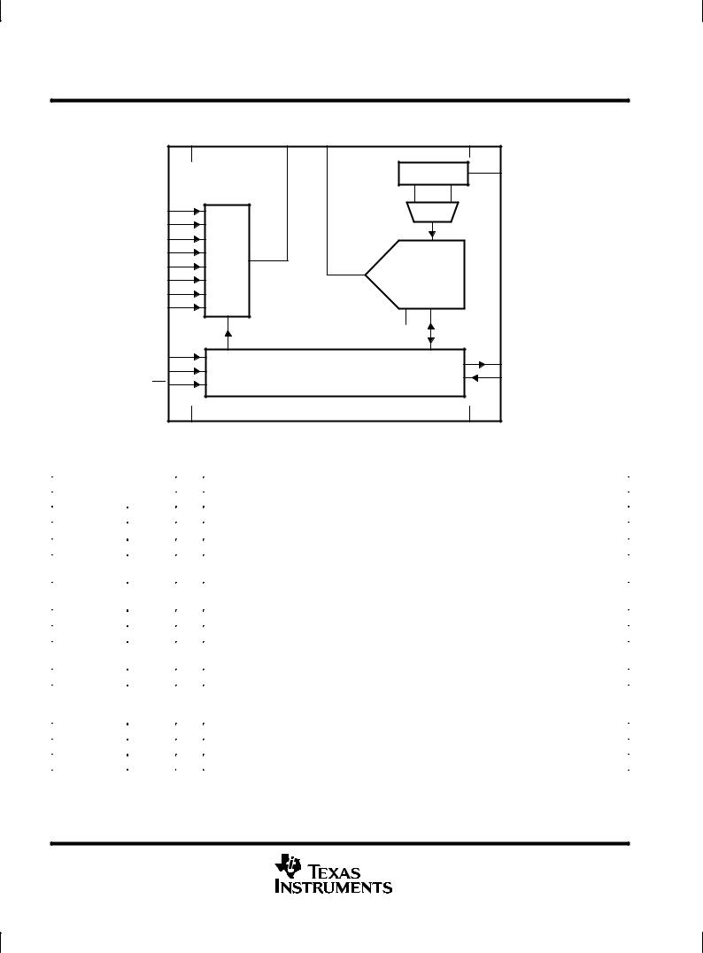
The TLV1570 is a 10-bit data acquisition system that combines an 8-channel input multiplexer (MUX), a high-speed 10-bit ADC, an on-chip reference, and a high-speed serial interface. The device contains an on-chip control register allowing control of channel selection, conversion start, reference voltage levels, and power down via the serial port. The MUX is independently accessible, which allows the user to insert a signal conditioning circuit such as an anti-aliasing filter or an amplifier, if required, between the MUX and the ADC. Therefore one signal conditioning circuit can be used for all eight channels.
The TLV1570 operates from a single 2.7-V to 5.5-V power supply. The device accepts an analog input range from 0 V to AVDD and digitizes the input at a maximum 1.25 MSPS throughput rate. Power dissipation is only 8 mW with a 2.7-V supply or 40 mW with a 5.5-V supply. The device features an auto-power down mode that automatically powers down to 300 μA, 10 ns after a conversion is performed. With software power down enabled, the device is further powered down to only 10 μA.
The TLV1570 communicates with digital microprocessors via a simple 4- or 5-wire serial port that interfaces directly to Texas Instruments TMS320 DSPs, and SPI and QSPI compatible microcontrollers without using additional glue logic.
A very high throughput rate, a simple serial interface, and low power consumption make the TLV1570 an ideal choice for high-speed digital signal processing requiring multiple analog inputs.
AVAILABLE OPTIONS
|
PACKAGED DEVICES |
|
TA |
|
|
SMALL OUTLINE |
SMALL OUTLINE |
|
|
(DW) |
(PW) |
|
|
|
0°C to 70°C |
TLV1570CDW |
TLV1570CPW |
|
|
|
± 40°C to 85°C |
TLV1570IDW |
TLV1570IPW |
Please be aware that an important notice concerning availability, standard warranty, and use in critical applications of Texas Instruments semiconductor products and disclaimers thereto appears at the end of this data sheet.
SPI and QSPI are trademarks of Motorola, Inc.
PRODUCTION DATA information is current as of publication date. Products conform to specifications per the terms of Texas Instruments standard warranty. Production processing does not necessarily include testing of all parameters.
Copyright 1998, Texas Instruments Incorporated
POST OFFICE BOX 655303 •DALLAS, TEXAS 75265 |
1 |
TLV1570
2.7 V TO 5.5 V 8-CHANNEL 10-BIT 1.25-MSPS SERIAL ANALOG-TO-DIGITAL CONVERTER
SLAS169A ± DECEMBER 1997± REVISED SEPTEMBER 1998
functional block diagram
AVDD |
MO |
AIN |
DVDD |
|
|
|
|
REFERENCE |
REF |
CH0 |
|
|
|
|
CH1 |
|
|
REF+ |
|
CH2 |
|
|
|
|
|
|
|
|
|
CH3 |
MUX |
|
|
|
CH4 |
|
10-BIT |
|
|
|
|
|
||
CH5 |
|
|
SAR ADC |
|
CH6 |
|
|
|
|
CH7 |
|
REF± |
|
|
|
|
|
||
|
|
|
AGND |
|
SCLK |
|
I/O REGISTERS |
|
SDOUT |
SDIN |
|
|
||
AND CONTROL LOGIC |
|
FS |
||
CS |
|
|||
|
|
|
|
|
AGND |
|
|
DGND |
|
|
|
|
|
|
Terminal Functions |
||||
|
|
|
|
|
|
|
|
|
|
|
|
TERMINAL |
I/O |
|
|
DESCRIPTION |
|||
|
|
NAME |
NO. |
|
|
||||
|
|
|
|
|
|
|
|
||
|
|
|
|
|
|
|
|
|
|
|
AGND |
14 |
|
Analog ground |
|||||
|
|
|
|
|
|
|
|
|
|
|
AIN |
20 |
I |
ADC analog input |
|||||
|
|
|
|
|
|
|
|
|
|
|
AVDD |
15 |
|
Analog supply voltage, 2.7 V to 5.5 V |
|||||
|
CH0 ± CH7 |
5,4,3,2,1, |
I |
Analog input channels 0 ± 7 |
|||||
|
|
|
18,17,16 |
|
|
|
|
|
|
|
|
|
|
|
|
|
|
|
|
|
|
|
12 |
I |
Chip Select. A low level signal on |
|
enables the TLV1570. A high level signal on |
|
disables the device |
|
CS |
|
CS |
CS |
|||||
|
|
|
|
|
and disconnects power to the TLV1570. |
||||
|
|
|
|
|
|||||
|
DGND |
7 |
|
Digital ground |
|||||
|
|
|
|
|
|||||
|
DVDD |
6 |
|
Digital supply voltage, 2.7 V to 5.5 V |
|||||
|
FS |
8 |
I |
Frame sync. The falling edge of the frame sync pulse from a DSP indicates the start of a serial data frame |
|||||
|
|
|
|
|
shifted out of the TLV1570. FS is pulled high when interfaced to a microcontroller. |
||||
|
|
|
|
|
|||||
|
MO |
19 |
O |
On-chip MUX analog output |
|||||
|
|
|
|
|
|||||
|
REF |
13 |
I |
Reference voltage input. The voltage applied to REF defines the input span of the TLV1570. In external |
|||||
|
|
|
|
|
reference mode, a 0.1 μF decoupling capacitor must be placed between the reference and AGND. This |
||||
|
|
|
|
|
is not required for internal reference mode. |
||||
|
|
|
|
|
|||||
|
SCLK |
9 |
I |
Serial clock input. SCLK synchronizes the serial data transfer and is also used for internal data conversion. |
|||||
|
|
|
|
|
|||||
|
SDIN |
10 |
I |
Serial data input used to configure the internal control register. |
|||||
|
|
|
|
|
|||||
|
SDOUT |
11 |
O |
Serial data output. A/D conversion results are output at SDOUT. |
|||||
2 |
POST OFFICE BOX 655303 •DALLAS, TEXAS 75265 |
TLV1570 2.7 V TO 5.5 V 8-CHANNEL 10-BIT 1.25-MSPS SERIAL ANALOG-TO-DIGITAL CONVERTER
SLAS169A ± DECEMBER 1997± REVISED SEPTEMBER 1998
detailed description
analog-to-digital converter
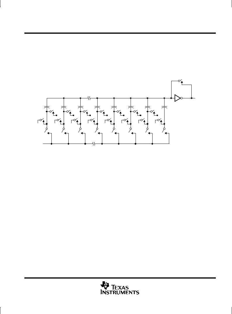
The TLV1570 ADC uses the SAR architecture described in this section. The CMOS threshold detector in the successive-approximation conversion system determines the value of each bit by examining the charge on a series of binary-weighted capacitors (see Figure 1). In the first phase of the conversion process, the analog input is sampled by closing the SC switch and all ST switches simultaneously. This action charges all of the capacitors to the input voltage.
SC
Threshold
Detector
To Output
Latches
512 |
256 |
128 |
8 |
4 |
2 |
1 |
1 |
|
Node 512 |
REF+ |
REF+ |
REF+ |
REF+ |
REF+ |
REF+ |
REF+ |
|
|
|
|||||||
REF ± |
REF ± |
REF ± |
REF ± |
REF ± |
REF ± |
REF ± |
REF ± |
|
|
ST |
ST |
ST |
ST |
ST |
ST |
ST |
ST |
VI
NOTE: REF± is tied to AGND
Figure 1. Simplified Model of the Successive-Approximation System
In the next phase of the conversion process, all ST and SC switches are opened and the threshold detector begins identifying bits by identifying the charge (voltage) on each capacitor relative to the reference (REF±) voltage (REF± is tied to AGND). In the switching sequence, ten capacitors are examined separately until all ten bits are identified and then the charge-convert sequence is repeated. In the first step of the conversion phase, the threshold detector looks at the first capacitor (weight = 512). Node 512 of this capacitor is switched to the REF+ voltage, and the equivalent nodes of all the other capacitors on the ladder are switched to REF±. If the voltage at the summing node is greater than the trip point of the threshold detector (approximately one-half VCC), a bit 0 is placed in the output register and the 512-weight capacitor is switched to REF±. If the voltage at the summing node is less than the trip point of the threshold detector, a bit 1 is placed in the register and the 512-weight capacitor remains connected to REF+ through the remainder of the successive-approximation process. The process is repeated for the 256-weight capacitor, the 128-weight capacitor, and so forth down the line until all bits are counted.
With each step of the successive-approximation process, the initial charge is redistributed among the capacitors. The conversion process relies on charge redistribution to count and weigh the bits from MSB to LSB.
In the case of the TLV1570, REF± is tied to ground and REF+ is connected to the REF input.
The TLV1570 can be programmed to use the on-chip internal reference (DI6=1). The user can select between two values of internal reference, 2.3 V or 3.8 V, using the control bit DI5.
During internal reference mode, the reference voltage is not output on the REF pin. Therefore it cannot be decoupled to analog ground (AGND), which acts as the negative reference for the ADC, using an external capacitor. Hence this mode requires the ground noise to be very low. The REF pin can be left open in this mode.
POST OFFICE BOX 655303 •DALLAS, TEXAS 75265 |
3 |

TLV1570
2.7 V TO 5.5 V 8-CHANNEL 10-BIT 1.25-MSPS SERIAL ANALOG-TO-DIGITAL CONVERTER
SLAS169A ± DECEMBER 1997± REVISED SEPTEMBER 1998
sampling frequency, fs
The TLV1570 requires 16 SCLKs for each sampling and conversion, therefore the equivalent maximum sampling frequency achievable with a given SCLK frequency is:
fs(MAX) = (1/16)fSCLK
power down
The TLV1570 offers two different power-down options. With auto power-down mode enabled, (DI4=0) the ADC proceeds to power down if FS is not detected on the 17th falling SCLK edge of a cycle (a cycle starts with FS being detected on a falling edge of SCLK) in DSP mode and after 16 SCLKs in μC mode. The TLV1570 will recover from auto power down when FS goes high in DSP mode or when the next SCLK comes in μC mode. In the case of software power down, the ADC goes to the software power-down state one cycle after CR.DI15 is set to 1. Unlike auto power down which recovers in 1 SCLK, software power down takes 16 SCLKs to recover.
|
|
|
SOFTWARE |
|
|
DESCRIPTION |
AUTO POWER DOWN |
POWERDOWN |
|
|
|
|
CS = DVDD |
|
Maximum power down dissipation current |
300 μA |
10 μA |
||
|
|
|
|
|
Comparator |
Power down |
Powerdown |
||
|
|
|
|
|
Clock buffer² |
Power down |
Powerdown |
||
Reference |
Active |
Powerdown |
||
|
|
|
|
|
Register |
Not saved |
Not saved |
||
|
|
|
|
|
Minimum power down time |
1 SCLK |
1 μs |
||
|
|
|
|
|
Minimum resume time |
1 SCLK |
800 ns |
||
|
|
|
|
|
Power down |
DSP mode |
No FS present one SCLK after previous conversion completed |
CR.DI15 set to 1 |
|
|
|
|
||
Microprocessor mode (FS = 1) |
SCLK stopped after previous conversion completed |
CR.DI15 set to 1 |
||
|
||||
|
|
|
|
|
Power up |
DSP mode |
FS present |
CR.DI15 set to 1 |
|
|
|
|
||
Microprocessor mode (FS = 1) |
SCLK present |
CR.DI15 set to 1 |
||
|
||||
² Only in DSP mode is input buffer of clock in power-down mode.
³ The software power down enable/disable bit is not acted until the start of the next cycle (see section configuring the TLV1570 for more information.
configuring the TLV1570
The TLV1570 is to be configured by writing the control bits to SDIN. The configuration will not take affect until the next cycle. A new configuration is needed for each conversion. Once the channel input and other options are selected, the conversion takes place in the next cycle. Conversion results are shifted out as conversion progresses ( see Figure 2).
|
One Cycle |
|
Second Cycle |
|
17 |
|
32 |
SCLK |
|
|
|
ts |
tconv |
ts |
tconv |
SDIN |
Configure Data 1 |
|
Configure Data 2 |
SDOUT |
Result 0 |
|
Result 1 |
Figure 2. TLV1570 Configuration Cycle Timing
4 |
POST OFFICE BOX 655303 •DALLAS, TEXAS 75265 |

TLV1570 2.7 V TO 5.5 V 8-CHANNEL 10-BIT 1.25-MSPS SERIAL ANALOG-TO-DIGITAL CONVERTER
SLAS169A ± DECEMBER 1997± REVISED SEPTEMBER 1998
configuration register (CR) definition
BIT |
|
DESCRIPTION |
|
5 V |
3 V |
|
|
|
|
|
|
|
|
|
Software power down: |
|
|
X |
X |
|
DI15 |
0: |
Normal |
|
|
X |
X |
|
1: |
Power down enabled |
|
|
||
|
|
|
|
|
||
|
|
|
|
|
||
DI14 |
Reads out values of the internal register, 1 ± read. Only DI15 ± DI1 are read out. |
X |
X |
|||
|
|
|
|
|
||
|
These two bits select the self-test voltage to be applied to the ADC input during next clock cycle: |
X |
X |
|||
|
00: |
Allow AIN to come in normally |
|
|
|
|
DI13, DI12 |
01: |
Apply AGND to AIN |
|
|
|
|
|
10: |
Apply VREF/2 to AIN |
|
|
|
|
|
11: |
N/A |
|
|
|
|
|
|
|
|
|
|
|
|
Choose speed application |
|
|
X |
X |
|
DI11 |
0: |
High speed (higher power consumption) |
|
|
|
|
|
1: |
Low speed (lower power consumption) |
|
|
|
|
|
|
|
|
|
|
|
|
This bit enables channel auto-scan function. |
|
|
X |
X |
|
DI10 |
0: |
Auto-scan disabled |
|
|
|
|
|
1: |
Auto-scan enabled |
|
|
|
|
|
|
|
|
|
||
|
DI9 ± DI7 These three bits select which of the eight |
DI9, DI8 These two bits select the channel swept |
X |
X |
||
|
channels is to be used (if DI10 = 0). |
sequence used by auto scan mode (if DI10 = 1) |
||||
|
|
|
||||
|
|
|
|
|
|
|
|
000: |
Channel 0 selected as input |
00: |
Analog inputs CH0, CH1, CH2, … .., CH7 |
|
|
|
sequentially selected |
|
|
|||
|
|
|
|
|
|
|
|
001: |
Channel 1 selected as input |
01: |
Analog inputs CH1, CH3, CH5, CH7 |
|
|
|
sequentially selected |
|
|
|||
|
|
|
|
|
|
|
|
010: |
Channel 2 selected as input |
10: |
Analog inputs CH0, CH2, CH4, CH6 |
|
|
DI9, DI8, DI7 |
sequentially selected |
|
|
|||
|
|
|
|
|
||
|
011: |
Channel 3 selected as input |
11: |
Analog inputs CH7, CH6, CH5, … .., CH0 |
|
|
|
sequentially selected |
|
|
|||
|
|
|
|
|
|
|
|
|
|
|
|
|
|
|
100: |
Channel 4 selected as input |
DI7 Auto-scan reset |
|
|
|
|
|
|
|
|
|
|
|
101: |
Channel 5 selected as input |
0: |
No reset |
|
|
|
110: |
Channel 6 selected as input |
1: |
Reset autoscan sequence |
|
|
|
111: |
Channel 7 selected as input |
|
|
|
|
|
|
|
|
|
|
|
|
Selects Internal or external reference voltage: |
|
|
X |
X |
|
DI6 |
0: |
External |
|
|
|
|
|
1: |
Internal |
|
|
|
|
|
|
|
|
|||
|
Selects internal reference voltage value to be applied to the ADC during next conversion cycle. |
|
|
|||
DI5 |
0: |
2.3 V |
|
|
|
X |
|
1: |
3.8 V |
|
|
X |
|
|
|
|
|
|
|
|
|
Enables/disables auto-power down function: |
|
|
X |
X |
|
DI4 |
1: |
Enable |
|
|
|
|
|
0: |
Disable |
|
|
|
|
|
|
|
|
|
|
|
|
Performance optimizer ± linearity |
|
|
|
|
|
DI3 |
0: AVDD = 5.5 V to 3.6 V |
|
|
X |
X |
|
|
1: AVDD = 3.5 V to 2.7 V |
|
|
|
|
|
DI2 |
Always write 0 (reserved bit) |
|
|
X |
X |
|
|
|
|
|
|
|
|
DI1 |
Always write 0 (reserved bit) |
|
|
X |
X |
|
|
|
|
|
|
|
|
DI0 |
Always write 0 (reserved bit) |
|
|
X |
X |
|
POST OFFICE BOX 655303 •DALLAS, TEXAS 75265 |
5 |

TLV1570
2.7 V TO 5.5 V 8-CHANNEL 10-BIT 1.25-MSPS SERIAL ANALOG-TO-DIGITAL CONVERTER
SLAS169A ± DECEMBER 1997± REVISED SEPTEMBER 1998
initialization-software sequence
This sequence shows the default settings, unless otherwise specified. The ADC requires that the user write to it every cycle. There is a cycle delay before control bits are implemented.
Example 1. Normal Sample Mode With Internal Reference
CYCLE |
WRITE TO |
CHANNEL |
OUPUT FROM |
COMMENT |
|
SDIN |
SAMPLED |
SDOUT |
|||
|
|
||||
|
|
|
|
|
|
1st |
0040h |
N/A |
Invalid |
No analog input channel sampled |
|
|
|
|
|
|
|
2nd |
01C0h |
N/A |
Invalid |
No analog input channel sampled |
|
|
|
|
|
|
|
3rd |
0040h |
3 |
From Channel 3 |
|
|
|
|
|
|
|
|
4th |
8040h |
0 |
From Channel 0 |
Software power down enabled |
|
|
|
|
|
|
|
5th |
0040h |
N/A |
Invalid |
Software power down mode, no analog input channel sampled |
|
|
|
|
|
|
|
Wait 800 ns |
|
|
Recovery time, no analog input channel sampled (16 SCLKs if AVDD = 5 V and |
||
|
|
fCLK = 20 MHz) |
|||
|
|
|
|
||
6th |
0140h |
N/A |
Invalid |
Recovery time, no analog input channel sampled |
|
|
|
|
|
|
|
7th |
0040h |
2 |
From Channel 2 |
|
|
Example 2. Auto Scan Mode
CYCLE |
WRITE TO |
CHANNEL |
OUTPUT FROM |
COMMENT |
|
SDIN |
SAMPLED |
SDOUT |
|||
|
|
||||
|
|
|
|
|
|
1st |
0480h |
N/A |
Invalid |
Auto-scan reset enabled, no analog input channel sampled |
|
|
|
|
|
|
|
2nd |
0480h |
N/A |
Invalid |
No analog input channel sampled |
|
|
|
|
|
|
|
3rd |
0400h |
0 |
From Channel 0 |
|
|
|
|
|
|
|
|
4th |
0400h |
1 |
From Channel 1 |
|
|
|
|
|
|
|
|
5th |
0400h |
2 |
From Channel 2 |
|
|
|
|
|
|
|
|
6th |
0400h |
3 |
From Channel 3 |
|
|
|
|
|
|
|
|
7th |
0400h |
4 |
From Channel 4 |
|
|
|
|
|
|
|
|
8th |
0400h |
5 |
From Channel 5 |
|
|
|
|
|
|
|
|
9th |
0400h |
6 |
From Channel 6 |
|
|
|
|
|
|
|
|
10th |
0400h |
7 |
From Channel 7 |
|
|
|
|
|
|
|
|
11th |
0400h |
0 |
From Channel 0 |
|
NOTE: If software power down is enabled during auto-scan mode, the next channel in the sequence is skipped.
6 |
POST OFFICE BOX 655303 •DALLAS, TEXAS 75265 |

TLV1570 2.7 V TO 5.5 V 8-CHANNEL 10-BIT 1.25-MSPS SERIAL ANALOG-TO-DIGITAL CONVERTER
SLAS169A ± DECEMBER 1997± REVISED SEPTEMBER 1998
initialization-software sequence (continued)
Example 3. Auto-Scan Mode
This example shows a change in sequence in the middle of the current sequence. The following shows that after the initial auto-scan reset, a reset is not necessary again when switching channel sequences.
CYCLE |
WRITE TO |
CHANNEL |
OUTPUT FROM |
COMMENT |
|
SDIN |
SAMPLED |
SDOUT |
|
|
|
|
|
|
1st |
0480h |
N/A |
N/A |
No analog input channel sampled |
|
|
|
|
|
2nd |
0480h |
N/A |
N/A |
Auto-scan reset enabled, no analog input channel sampled |
|
|
|
|
|
3rd |
0400h |
0 |
From Channel 0 |
Start of sequence 0 |
|
|
|
|
|
4th |
0700h |
1 |
From Channel 1 |
Enable channel sequence 3 (no auto-scan reset required) |
|
|
|
|
|
5th |
0700h |
7 |
From Channel 7 |
Start of sequence 3 |
|
|
|
|
|
6th |
0700h |
6 |
From Channel 6 |
|
|
|
|
|
|
7th |
0700h |
5 |
From Channel 5 |
|
|
|
|
|
|
8th |
0700h |
4 |
From Channel 4 |
|
|
|
|
|
|
9th |
0700h |
3 |
From Channel 3 |
|
|
|
|
|
|
10th |
0700h |
2 |
From Channel 2 |
|
|
|
|
|
|
11th |
0700h |
1 |
From Channel 1 |
|
|
|
|
|
|
12th |
0700h |
0 |
From Channel 0 |
|
Example 4. Auto-Scan Mode
This example shows a switch in sequence in the course of a sequence. The following shows that a particular sequence does not have to be continued if remaining channels do not need to be sampled (i.e., only channel 1 through channel 5 sampled, not channels 6, 7, 8)
CYCLE |
WRITE TO |
CHANNEL |
OUPUT FROM |
COMMENT |
|
SDIN |
SAMPLED |
SDOUT |
|
|
|
|
|
|
1st |
0480h |
N/A |
N/A |
No analog input channel sampled |
|
|
|
|
|
2nd |
0480h |
N/A |
N/A |
Auto-scan reset enabled, no analog input channel sampled |
|
|
|
|
|
3rd |
0400h |
0 |
From Channel 0 |
|
|
|
|
|
|
4th |
0400h |
1 |
From Channel 1 |
|
|
|
|
|
|
5th |
0400h |
2 |
From Channel 2 |
|
|
|
|
|
|
6th |
0400h |
3 |
From Channel 3 |
|
|
|
|
|
|
7th |
0400h |
4 |
From Channel 4 |
|
|
|
|
|
|
8th |
0480h |
5 |
From Channel 5 |
Auto-scan reset enabled |
|
|
|
|
|
9th |
0400h |
0 |
From Channel 0 |
Sequence is reset to channel 0 |
|
|
|
|
|
10th |
0400h |
1 |
From Channel 1 |
|
|
|
|
|
|
11th |
0400h |
2 |
From Channel 2 |
|
The TLV1570 is a 800-ns 10-bit 8-analog input channel analog-to-digital converter with a throughput of up to 1.25 MSPS at 5 V and up to 625 KSPS at 3 V respectively. To run at its fastest conversion rate, it must be clocked at 20 MHz at 5-V or 10 MHz at 3-V. The TLV1570 can be easily interfaced to microcontrollers, ASICs, DSPs, or shift registers. The TLV1570 serial interface is designed to be fully compatible with Serial Peripheral Interface (SPI) and TMS320 DSP serial ports. No additional hardware is required to interface between the TLV1570 and a microcontroller (μCs) with a SPI serial port or a TMS320 DSP. However, the speed is limited by the SCLK rate of the μC or the DSP.
POST OFFICE BOX 655303 •DALLAS, TEXAS 75265 |
7 |
TLV1570
2.7 V TO 5.5 V 8-CHANNEL 10-BIT 1.25-MSPS SERIAL ANALOG-TO-DIGITAL CONVERTER
SLAS169A ± DECEMBER 1997± REVISED SEPTEMBER 1998
initialization-software sequence (continued)
The TLV1570 interfaces to a DSP over five lines: CS, SCLK, SDOUT, SDIN, and FS, and interfaces to a μC over four lines: CS, SCLK, SDOUT, and SDIN. The FS input should be pulled high in μC mode. The device is in 3-state and power-down mode when CS is high. After CS falls, the TLV1570 checks the FS input at the CS falling edge to determine the operation mode. If FS is low, DSP mode is set, otherwise μC mode is set.
TLV1570 |
TMS320 |
CS |
XF |
SCLK |
CLKX |
|
CLKR |
FS |
FSX |
|
FSR |
SDIN |
DX |
SDOUT |
DR |
Figure 3. DSP to TLV1570 Interface
TLV1570 μC
CS  I/O Terminal
SCLK  SCLK
SCLK
FS DVDD
SDIN  DX
DX
SDOUT  DR
DR
Figure 4. μC to TLV1570 Interface
grounding and decoupling considerations
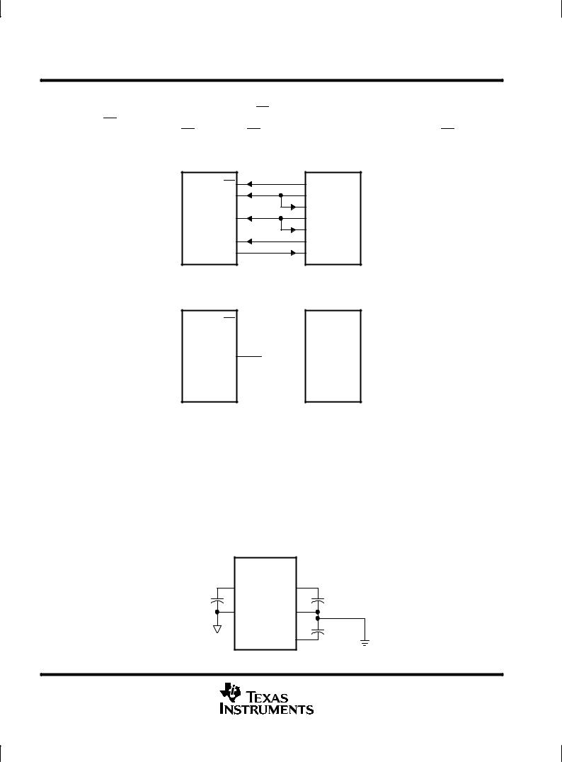
General practices should apply to the PCB design to limit high frequency transients and noise that are fed back into the supply and reference lines (see Figure 5). This requires that the supply and reference pins be sufficiently bypassed. In most cases 0.1 μF ceramic chip capacitors are adequate to keep the impedance low over a wide frequency range. Since their effectiveness depends largely on the proximity to the individual supply pin. They should be placed as close to the supply pins as possible.
To reduce high frequency and noise coupling, it is highly recommended that digital and analog ground be shorted immediately outside the package. This can be accomplished by running a low impedance line between DGND and AGND, under the package.
TLV1570 |
|
DVDD |
AV |
|
DD |
100 nF |
100 nF |
DGND |
AGND |
100 nF
REF
Figure 5. Placement of Decoupling Capacitors
8 |
POST OFFICE BOX 655303 •DALLAS, TEXAS 75265 |

TLV1570 2.7 V TO 5.5 V 8-CHANNEL 10-BIT 1.25-MSPS SERIAL ANALOG-TO-DIGITAL CONVERTER
SLAS169A ± DECEMBER 1997± REVISED SEPTEMBER 1998
power supply ground layout
Printed circuit boards that use separate analog and digital ground planes offer the best system performance. Wire-wrap boards do not perform well and should not be used. The two ground planes should be connected together at the low-impedance power-supply source. The best ground connection may be achieved by connecting the ADC AGND terminal to the system analog ground plane making sure that analog ground currents are well managed.
simplified analog input analysis
Using the equivalent circuit in Figure 6, the time required to charge the analog input capacitance from 0 to VS within 1/2 LSB, tch(1/2 LSB), can be derived as follows:
The capacitance charging voltage is given by:
VC(t) + VS 1±e±tch RtCi
where
Rt = Rs + Ri (1)
Ri = Ri(ADC) + Ri(MUX)
tch = Charge time
The input impedance Ri is 718 W at 5 V, and is higher (~ 1.25 kW) at 2.7 V. The final voltage to 1/2 LSB is given by:
VC (1/2 LSB) = VS ± (VS /2048) |
(2) |
|||||
Equating equation 1 to equation 2 and solving for cycle time tc gives: |
|
|||||
V |
S * |
V |
2048 + V |
S |
1±e±tch RtCi |
|
|
|
S |
|
|
||
and time to change to 1/2 LSB (minimum sampling time) is: |
(3) |
|||||
|
||||||
tch (1/2 LSB) = Rt × Ci × ln(2048) |
|
|||||
where |
|
|
|
|
|
|
ln(2048) = 7.625 |
|
|
|
|||
Therefore, with the values given, the time for the analog input signal to settle is: |
|
|||||
tch (1/2 LSB) = (Rs + 718 W) ×15 pF ×ln(2048) |
(4) |
|||||
This time must be less than the converter sample time shown in the timing diagrams. Which is 6x SCLK.
tch (1/2 LSB) ≤ 6x 1/f(SCLK) |
(5) |
Therefore the maximum SCLK frequency is: |
|
Max(f(SCLK) ) = 6/tch (1/2 LSB) = 6/(ln(2048) ×Rt ×Ci ) |
(6) |
POST OFFICE BOX 655303 •DALLAS, TEXAS 75265 |
9 |
 Loading...