


Texas Instruments TLV5619QDWR, TLV5619QDW, TLV5619IPWR, TLV5619IPW, TLV5619IDWR Datasheet
...TLV5619 2.7 V TO 5.5 V 12-BIT PARALLEL DIGITAL-TO-ANALOG CONVERTER WITH POWER DOWN
SLAS172C ± DECEMBER 1997 ± REVISED APRIL 2000
DSingle Supply 2.7-V to 5.5-V Operation
D±0.4 LSB Differential Nonlinearity (DNL),
±1.5 LSB Integral Nonlinearity (INL)
D12-Bit Parallel Interface
DCompatible With TMS320 DSP
DInternal Power On Reset
DSettling Time 1 µs Typ
DLow Power Consumption:
±8 mW for 5-V Supply
±4.3 mW for 3-V Supply
DReference Input Buffers
DVoltage Output
DMonotonic Over Temperature
DAsynchronous Update
description
The TLV5619 is a 12-bit voltage output DAC with a microprocessor and TMS320 compatible parallel interface. The 12 data bits are double buffered so that the output can be updated
asynchronously using the LDAC pin. During normal operation, the device dissipates 8 mW at a 5-V supply and 4.3 mW at a 3-V supply. The power consumption can be lowered to 50 nW by setting the DAC to power-down mode.
The output voltage is buffered by a ×2 gain rail-to-rail amplifier, which features a Class A output stage to improve stability and reduce settling time.
applications
DBattery Powered Test Instruments
DDigital Offset and Gain Adjustment
DBattery Operated/Remote Industrial Controls
DMachine and Motion Control Devices
DCordless and Wireless Telephones
DSpeech Synthesis
DCommunication Modulators
DArbitrary Waveform Generation
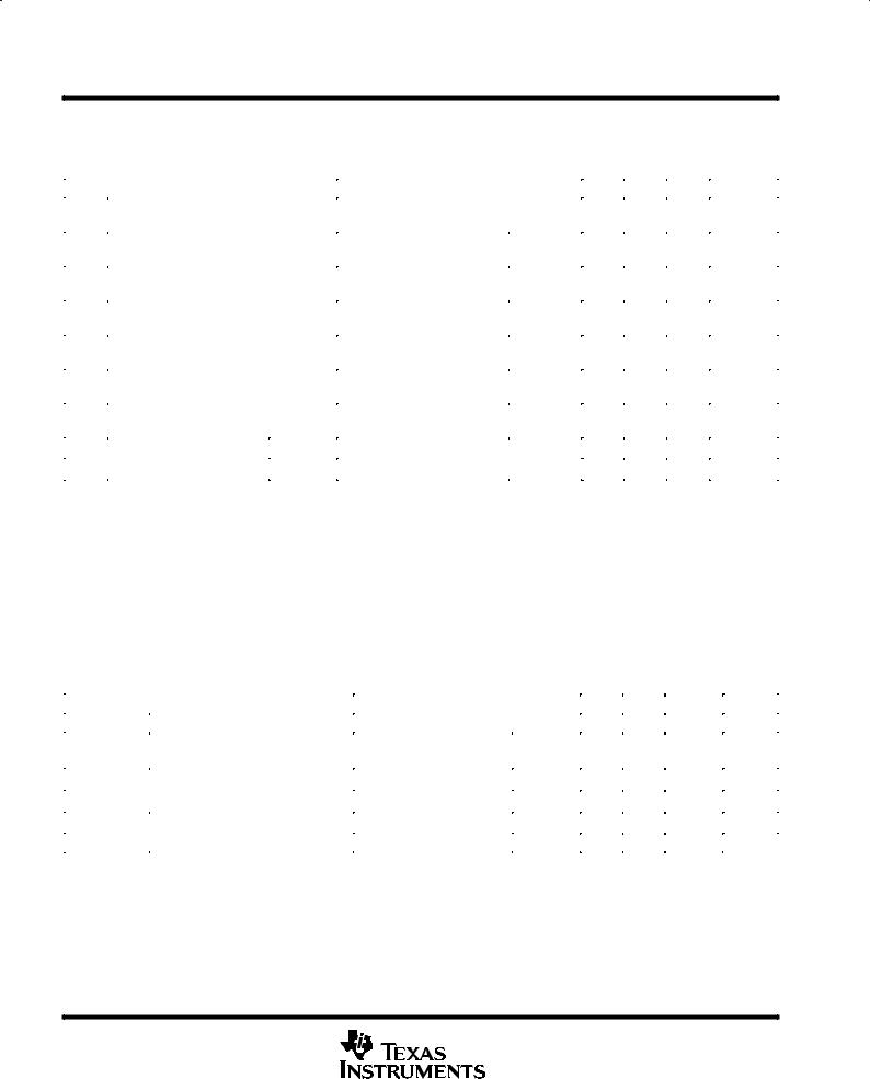
DW OR PW PACKAGE
(TOP VIEW)
|
|
|
|
|
|
|
|
|
|
|
|
D2 |
|
|
|
1 |
20 |
|
|
|
|
D1 |
|
D3 |
|
|
|
2 |
19 |
|
|
|
|
D0 |
|
|
|
|
|
|
|||||||
D4 |
|
|
3 |
18 |
|
|
|
|
CS |
||
|
|
|
|
|
|||||||
D5 |
|
|
4 |
17 |
|
|
|
|
WE |
||
|
|
|
|
|
|||||||
D6 |
|
|
|
5 |
16 |
|
|
|
|
|
|
|
|
|
|
|
|
|
LDAC |
|
|||
|
|
|
|
|
|
||||||
D7 |
|
|
|
6 |
15 |
|
|
|
|
PD |
|
|
|
|
|
|
|||||||
D8 |
|
|
|
7 |
14 |
|
|
|
|
GND |
|
|
|
|
|
|
|||||||
D9 |
|
|
|
8 |
13 |
|
|
|
|
OUT |
|
|
|
|
|
|
|||||||
D10 |
|
|
|
9 |
12 |
|
|
|
|
REFIN |
|
|
|
|
|
|
|||||||
D11 |
|
|
|
10 |
11 |
|
|
|
|
VDD |
|
|
|
|
|
|
|||||||
|
|
|
|
|
|||||||
|
|
|
|
|
|
|
|
|
|
|
|
AVAILABLE OPTIONS
PACKAGE
TA |
SMALL OUTLINE |
TSSOP |
|
(DW) |
(PW) |
||
|
|||
|
|
|
|
0°C to 70°C |
TLV5619CDW |
TLV5619CPW |
|
|
|
|
|
± 40°C to 85°C |
TLV5619IDW |
TLV5619IPW |
|
|
|
|
|
± 40°C to 125°C |
TLV5619QDW |
Ð |
|
|
|
|
Please be aware that an important notice concerning availability, standard warranty, and use in critical applications of Texas Instruments semiconductor products and disclaimers thereto appears at the end of this data sheet.
PRODUCTION DATA information is current as of publication date. Products conform to specifications per the terms of Texas Instruments standard warranty. Production processing does not necessarily include testing of all parameters.
Copyright 2000, Texas Instruments Incorporated
POST OFFICE BOX 655303 •DALLAS, TEXAS 75265 |
1 |

TLV5619
2.7 V TO 5.5 V 12-BIT PARALLEL DIGITAL-TO-ANALOG CONVERTER WITH POWER DOWN
SLAS172C ± DECEMBER 1997 ± REVISED APRIL 2000
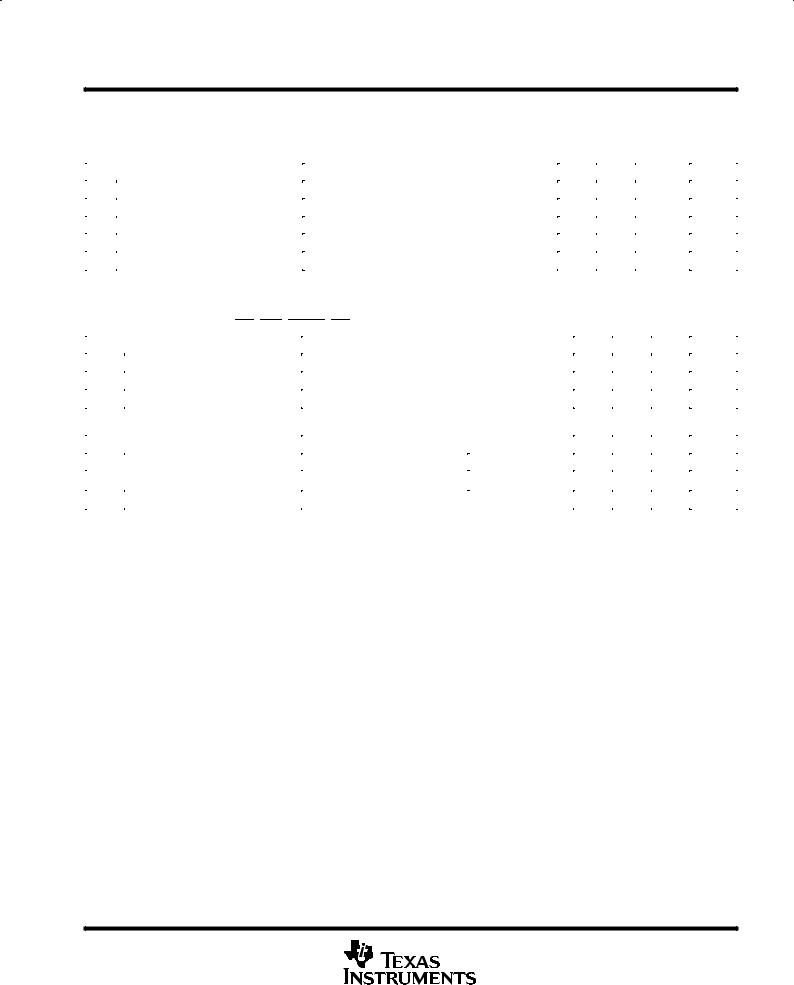
functional block diagram
REFIN |
12 |
+ |
|
|
|
_ |
|
|
|
D0 |
19 |
|
|
|
|
D1 |
20 |
|
|
|
|
D2 |
1 |
|
|
Resistor |
|
2 |
|
|
String DAC |
|
|
D3 |
|
|
|
||
D4 |
3 |
|
12 |
|
|
D5 |
4 |
12-Bit |
12-Bit |
12 |
13 |
|
5 |
Input |
DAC |
||
D6 |
x2 |
OUT |
|||
D7 |
6 |
Register |
Latch |
|
|
|
|
|
|
||
D8 |
7 |
|
|
|
|
D9 |
8 |
|
|
|
|
D10 |
9 |
|
|
|
|
D11 |
10 |
|
|
|
|
|
|
|
|
Power-On |
|
|
|
|
|
|
|
|
|
18 |
|
|
Select |
|
|
|
Reset |
|||||||||
|
|
|
|
|
|
|
|
|
|
|
and |
|
|
|
|
|
||||||||
|
|
|
|
|
CS |
|
|
|
Control |
|
|
|
|
|
||||||||||
|
|
|
|
|
|
|
|
|||||||||||||||||
|
|
|
|
|
|
|
17 |
|
|
|
|
|
|
|
||||||||||
|
|
|
|
|
WE |
|
|
|
|
|
|
Logic |
|
|
|
|
|
|||||||
|
|
|
|
|
|
|
|
|
||||||||||||||||
|
|
|
|
|
|
|
|
|
|
|
|
|
|
|
|
|
|
|
|
|
|
|
|
|
|
|
|
|
|
|
|
|
|
|
|
|
|
|
|
|
|
|
15 |
|
16 |
|
|
||
|
|
|
|
|
|
|
|
|
|
|
|
|
|
|
|
|
|
|||||||
|
|
|
|
|
|
|
|
|
|
|
|
|
|
|
PD |
|
LDAC |
|
||||||
|
|
|
|
|
|
|
|
|
|
|
|
|
|
|
|
|
|
|
|
Terminal Functions |
||||
|
|
|
|
|
|
|
|
|
|
|
|
|
|
|
|
|
|
|
|
|
||||
|
|
|
|
|
|
TERMINAL |
|
I/O |
|
|
|
|
|
|
|
|
DESCRIPTION |
|||||||
|
|
|
|
NAME |
NO. |
|
|
|
|
|
|
|
|
|||||||||||
|
|
|
|
|
|
|
|
|
|
|
|
|
|
|
|
|
||||||||
|
|
|
|
|
|
|
|
|
|
|
|
|
|
|
|
|||||||||
|
|
|
|
|
|
|
|
|
|
|
18 |
|
I |
|
|
|
|
Chip select |
|
|
|
|
||
|
CS |
|
|
|
|
|
|
|
|
|
|
|
|
|||||||||||
|
|
|
|
|
|
|
|
|
|
|
|
|
|
|
|
|
|
|
|
|
|
|
|
|
|
D0 (LSB)±D11 (MSB) |
19, 20, |
|
I |
|
|
|
|
Parallel data input |
|
|
|
|
|||||||||||
|
1 ± 10 |
|
|
|
|
|
|
|
|
|
||||||||||||||
|
|
|
|
|
|
|
|
|
|
|
|
|
|
|
|
|
|
|
|
|
|
|
|
|
|
|
|
|
|
|
|
|
|
|
|
|
|
|
|
|
|||||||||
|
GND |
14 |
|
|
|
|
|
|
Ground |
|
|
|
|
|||||||||||
|
|
|
|
|
|
|
|
|
|
|
|
|
|
|
||||||||||
|
|
|
|
|
|
|
|
|
|
|
16 |
|
I |
|
|
|
|
Load DAC |
|
|
|
|
||
|
LDAC |
|
|
|
|
|
|
|
|
|
|
|||||||||||||
|
|
|
|
|
|
|
|
|
|
|
|
|
|
|||||||||||
|
OUT |
13 |
O |
|
|
|
|
Analog output |
|
|
|
|
||||||||||||
|
|
|
|
|
|
|
|
|
|
|
||||||||||||||
|
|
|
|
|
|
|
|
|
|
|
15 |
|
I |
|
|
|
|
When low, disables all buffer amplifier voltages to reduce supply current |
||||||
|
PD |
|
|
|
|
|
|
|
||||||||||||||||
|
|
|
|
|
|
|
|
|
|
|
|
|
|
|
||||||||||
|
REFIN |
12 |
|
I |
|
|
|
|
Voltage reference input |
|
|
|
|
|||||||||||
|
|
|
|
|
|
|
|
|
|
|
|
|
|
|
||||||||||
|
VDD |
11 |
|
|
|
|
|
|
Positive power supply |
|
|
|
|
|||||||||||
|
|
|
|
|
|
|
|
|
|
|
17 |
|
I |
|
|
|
|
Write enable |
|
|
|
|
||
|
WE |
|
|
|
|
|
|
|
|
|
|
|||||||||||||
2 |
POST OFFICE BOX 655303 •DALLAS, TEXAS 75265 |

TLV5619 2.7 V TO 5.5 V 12-BIT PARALLEL DIGITAL-TO-ANALOG CONVERTER WITH POWER DOWN
SLAS172C ± DECEMBER 1997 ± REVISED APRIL 2000
absolute maximum ratings over operating free-air temperature range (unless otherwise noted)²
Supply voltage (VDD to GND) . . . . . . . . . . . . . . . . . . . . . . . . . . . . . . . . . . . . . . . . . . . . . . . |
. . . . . . . . . . . . . . . . . 7 |
V |
Analog input voltage range . . . . . . . . . . . . . . . . . . . . . . . . . . . . . . . . . . . . . . . . . . . . . . . . . . |
± 0.3 V to VDD + 0.3 |
V |
Reference input voltage . . . . . . . . . . . . . . . . . . . . . . . . . . . . . . . . . . . . . . . . . . . . . . . . . . . . . |
. . . . . . . . VDD + 0.3 |
V |
Digital input voltage range to GND . . . . . . . . . . . . . . . . . . . . . . . . . . . . . . . . . . . . . . . . . . . |
± 0.3 V to VDD + 0.3 |
V |
Operating free-air temperature range, TA: TLV5619C . . . . . . . . . . . . . . . . . . . . . . . . . . . . |
. . . . . . . . 0°C to 70°C |
|
TLV5619I . . . . . . . . . . . . . . . . . . . . . . . . . . . . . |
. . . . . . ±40°C to 85°C |
|
TLV5619Q . . . . . . . . . . . . . . . . . . . . . . . . . . . . |
. . . . . ±40°C to 125°C |
|
Storage temperature range, Tstg . . . . . . . . . . . . . . . . . . . . . . . . . . . . . . . . . . . . . . . . . . . . . . |
. . . . . ±65°C to 150°C |
|
Lead temperature 1,6 mm (1/16 inch) from case for 10 seconds . . . . . . . . . . . . . . . . . . |
. . . . . . . . . . . . . 260°C |
|
²Stresses beyond those listed under ªabsolute maximum ratingsº may cause permanent damage to the device. These are stress ratings only, and functional operation of the device at these or any other conditions beyond those indicated under ªrecommended operating conditionsº is not implied. Exposure to absolute-maximum-rated conditions for extended periods may affect device reliability.
recommended operating conditions
|
|
MIN |
NOM |
MAX |
UNIT |
|
|
|
|
|
|
Supply voltage, VDD (5-V Supply) |
|
4.5 |
5 |
5.5 |
V |
Supply voltage, VDD (3-V Supply) |
|
2.7 |
3 |
3.3 |
V |
High-level digital input voltage, VIH |
VDD |
2 |
|
|
V |
Low-level digital input voltage, VIL |
VDD |
|
|
0.8 |
V |
Reference voltage, Vref to REFIN terminal (5-V Supply) |
0 |
2.048 |
VDD ± 1.5 |
V |
|
Reference voltage, Vref to REFIN terminal (3-V Supply) |
0 |
1.024 |
VDD ± 1.5 |
V |
|
Load resistance, RL |
|
2 |
10 |
|
kΩ |
Load capacitance, CL |
|
|
|
100 |
pF |
|
TLV5619C |
0 |
|
70 |
|
Operating free-air temperature, TA |
|
|
|
|
°C |
TLV5619I |
± 40 |
|
85 |
||
|
TLV5619Q |
± 40 |
|
125 |
|
|
|
|
|
|
|
NOTES: 1. The recommended operating levels for both VIH and VIL apply to all valid values of VDD.
2. Reference input voltages greater than VDD/2 will cause output saturation for large DAC codes.
POST OFFICE BOX 655303 •DALLAS, TEXAS 75265 |
3 |
TLV5619
2.7 V TO 5.5 V 12-BIT PARALLEL DIGITAL-TO-ANALOG CONVERTER WITH POWER DOWN
SLAS172C ± DECEMBER 1997 ± REVISED APRIL 2000
electrical characteristics over recommended operating free-air temperature range, supply voltages, and reference voltages (unless otherwise noted)
static DAC specifications
|
PARAMETER |
TEST CONDITIONS |
|
MIN |
TYP |
MAX |
UNIT |
|||
|
|
|
|
|
|
|
|
|
|
|
|
Resolution |
Vref(REFIN) = 2.048 V at 5 |
V, |
|
12 |
|
|
bits |
||
|
1.024 |
V at 3 |
V |
|
|
|
||||
|
|
|
|
|
|
|
|
|||
|
|
|
|
|
|
|
|
|
|
|
|
Integral nonlinearity (INL) |
Vref(REFIN) = 2.048 V at 5 |
V, |
See Note 3 |
|
± 1.5 |
± 4 |
LSB |
||
|
1.024 |
V at 3 |
V, |
|
||||||
|
|
|
|
|
|
|
|
|||
|
|
|
|
|
|
|
|
|
|
|
|
Differential nonlinearity (DNL) |
Vref(REFIN) = 2.048 V at 5 |
V, |
See Note 4 |
|
± 0.4 |
± 1 |
LSB |
||
|
1.024 |
V at 3 |
V, |
|
||||||
|
|
|
|
|
|
|
|
|||
|
|
|
|
|
|
|
|
|
|
|
EZS |
Zero-scale error (offset error at zero scale) |
Vref(REFIN) = 2.048 V at 5 |
V, |
See Note 5 |
|
± 3 |
± 20 |
mV |
||
1.024 |
V at 3 |
V, |
|
|||||||
|
|
|
|
|
|
|
|
|||
|
|
|
|
|
|
|
|
|
|
|
|
Zero-scale-error temperature coefficient |
Vref(REFIN) = 2.048 V at 5 |
V, |
See Note 6 |
|
3 |
|
ppm/°C |
||
|
1.024 V at 3 |
V, |
|
|
||||||
|
|
|
|
|
|
|
|
|||
|
|
|
|
|
|
|
|
|
|
|
EG |
Gain error |
Vref(REFIN) = 2.048 V at 5 |
V, |
See Note 7 |
|
± 0.25 |
± 0.5 |
% of FS |
||
1.024 V at 3 |
V, |
|
voltage |
|||||||
|
|
|
|
|
|
|
||||
|
|
|
|
|
|
|
|
|
|
|
|
Gain error temperature coefficient |
Vref(REFIN) = 2.048 V at 5 |
V, |
See Note 8 |
|
1 |
|
ppm/°C |
||
|
1.024 V at 3 |
V, |
|
|
||||||
|
|
|
|
|
|
|
|
|||
|
|
|
|
|
|
|
|
|
|
|
PSRR |
Power-supply rejection ratio |
Zero scale |
See Notes 9 and 10 |
|
|
|
|
65 |
|
dB |
|
|
|
|
|
|
|
||||
Gain |
|
|
|
|
65 |
|
||||
|
|
|
|
|
|
|
|
|
||
|
|
|
|
|
|
|
|
|
|
|
NOTES: 3. The relative accuracy or integral nonlinearity (INL), sometimes referred to as linearity error, is the maximum deviation of the output from the line between zero and full scale excluding the effects of zero code and full-scale errors.
4.The differential nonlinearity (DNL), sometimes referred to as differential error, is the difference between the measured and ideal 1 LSB amplitude change of any two adjacent codes. Monotonic means the output voltage changes in the same direction (or remains constant) as a change in the digital input code.
5.Zero-scale error is the deviation from zero voltage output when the digital input code is zero.
6.Zero-scale-error temperature coefficient is given by: EZS TC = [EZS (Tmax) ± EZS (Tmin)]/Vref × 106/(Tmax ± Tmin).
7.Gain error is the deviation from the ideal output (2 ×Vref ± 1 LSB) with an output load of 10 kΩ excluding the effects of the zero-error.
8.Gain temperature coefficient is given by: EG TC = [EG(Tmax) ± EG (Tmin)]/Vref × 106/(Tmax ± Tmin).
9.Zero-scale-error rejection ratio (EZS-RR) is measured by varying the VDD from 4.5 V to 5.5 V dc and measuring the proportion of this signal imposed on the zero-code output voltage.
10.Gain-error rejection ratio (EG-RR) is measured by varying the VDD from 4.5 V to 5.5 V dc and measuring the proportion of this signal imposed on the full-scale output voltage after subtracting the zero scale change.
output specifications
|
PARAMETER |
TEST CONDITIONS |
MIN TYP |
MAX |
UNIT |
|
|
|
|
|
|
|
|
VO |
Voltage output range |
RL = 10 kΩ |
|
0 |
VDD±0.4 |
V |
|
Output load regulation accuracy |
VO(OUT) = 4.096 V, |
RL = 2 kΩ |
0.1 |
0.29 |
% of FS |
|
2.048 V |
voltage |
||||
|
|
|
|
|
|
|
IOSC(source) |
Output short circuit source current |
VO(OUT) = 0 V, |
5-V Supply |
100 |
|
mA |
|
|
|
||||
Full scale code |
3-V Supply |
25 |
|
|||
|
|
|
|
|||
|
|
|
|
|
||
|
|
|
|
|
|
|
IO(source) |
Output source current |
RL = 100 Ω |
5-V Supply |
10 |
|
mA |
|
|
|
||||
3-V Supply |
10 |
|
||||
|
|
|
|
|
||
|
|
|
|
|
|
|
4 |
POST OFFICE BOX 655303 •DALLAS, TEXAS 75265 |
TLV5619 2.7 V TO 5.5 V 12-BIT PARALLEL DIGITAL-TO-ANALOG CONVERTER WITH POWER DOWN
SLAS172C ± DECEMBER 1997 ± REVISED APRIL 2000
electrical characteristics over recommended operating free-air temperature range, supply voltages, and reference voltages (unless otherwise noted)
reference input (REFIN)
|
PARAMETER |
TEST CONDITIONS |
MIN TYP |
MAX |
UNIT |
|
|
|
|
|
|
Vref |
Reference input voltage |
See Note 11 |
0 |
VDD± 1.5 |
V |
Ri |
Reference input resistance |
|
10 |
|
MΩ |
Ci |
Reference input capacitance |
|
5 |
|
pF |
|
Reference feed through |
REFIN = 1 Vpp at 1 kHz + 1.024 V dc (see Note 12) |
±60 |
|
dB |
|
Reference input bandwidth |
REFIN = 0.2 Vpp + 1.024 V dc at ±3 dB |
1.4 |
|
MHz |
NOTES: 11. Reference input voltages greater than VDD/2 will cause output saturation for large DAC codes.
12.Reference feedthrough is measured at the DAC output with an input code = 0x000 and a Vref(REFIN) input = 1.024 V dc + 1 Vpp at 1 kHz.
digital inputs (D0 ± D11, CS, WE, LDAC, PD)
|
PARAMETER |
TEST CONDITIONS |
MIN TYP |
MAX |
UNIT |
|
|
|
|
|
|
IIH |
High-level digital input current |
VI = VDD |
|
1 |
µA |
IIL |
Low-level digital input current |
VI = 0 V |
|
±1 |
µA |
Ci |
Input capacitance |
|
8 |
|
pF |
power supply
PARAMETER |
TEST CONDITIONS |
|
MIN TYP |
MAX |
UNIT |
|
|
|
|
|
|
|
|
IDD Power supply current |
No load, All inputs 0 V or VDD |
5-V Supply |
1.6 |
3 |
mA |
|
|
|
|
||||
3-V Supply |
1.44 |
2.7 |
||||
|
|
|
||||
|
|
|
|
|
|
|
Power down supply current |
|
|
0.01 |
10 |
µA |
|
|
|
|
|
|
|
POST OFFICE BOX 655303 •DALLAS, TEXAS 75265 |
5 |
TLV5619
2.7 V TO 5.5 V 12-BIT PARALLEL DIGITAL-TO-ANALOG CONVERTER WITH POWER DOWN
SLAS172C ± DECEMBER 1997 ± REVISED APRIL 2000
operating characteristics over recommended operating free-air temperature range, supply voltages, and reference voltages (unless otherwise noted)
analog output dynamic performance
|
PARAMETER |
TEST CONDITIONS |
|
MIN |
TYP |
MAX |
UNIT |
|
|
|
|
|
|
|
|
|
|
|
|
CL = 100 pF, |
Vref(REFIN) = 2.048 V, |
5-V |
8 |
12 |
|
V/µs |
|
|
Supply |
|
|||||
SR |
Slew rate |
RL = 10 kΩ, |
1.024 V, |
|
|
|
|
|
|
|
|
|
|
||||
Code 32 to code 4095, |
VO from 10% to 90% |
3-V |
6 |
9 |
|
V/µs |
||
|
|
|
||||||
|
|
Code 4095 to code 32, |
90% to 10% |
Supply |
|
|||
|
|
|
|
|
|
|||
|
|
|
|
|
|
|
|
|
ts |
Output settling time (full scale) |
To ± 0.5 LSB, |
CL = 100 pF, |
|
|
1 |
3 |
µs |
RL = 10 kΩ, |
See Note 13 |
|
|
|||||
|
|
|
|
|
|
|
||
|
Glitch energy |
DIN = all 0s to all 1s |
|
|
|
5 |
|
nV±s |
|
|
|
|
|
|
|
|
|
|
|
fs = 480 kSPS, |
fOUT = 1 kHz, |
5-V |
|
|
|
|
S/N |
Signal to noise |
BW = 20 kHz, |
RL = 10 kΩ |
65 |
78 |
|
|
|
Supply |
|
|
||||||
|
|
CL = 100 pF, |
TA = 25°C, See Note 14 |
|
|
|
|
|
|
|
|
|
|
|
|
||
|
|
fs = 480 kSPS, |
fOUT = 1 kHz, |
5-V |
58 |
67 |
|
|
|
|
Supply |
|
|
||||
|
|
|
|
|
|
|||
S/(N+D) |
Signal to noise + distortion |
BW = 20 kHz, |
RL = 10 kΩ, |
|
|
|
|
|
3-V |
|
|
|
|
||||
|
|
CL = 100 pF, |
TA = 25°C, See Note 14 |
58 |
69 |
|
|
|
|
|
Supply |
|
dB |
||||
|
|
|
|
|
|
|
||
|
|
|
|
|
|
|
|
|
|
|
fs = 480 kSPS, |
fOUT = 1 kHz, |
|
|
|
|
|
|
Total harmonic distortion |
BW = 20 kHz, |
RL = 10 kΩ, |
|
|
±68 |
±60 |
|
|
|
CL = 100 pF, |
TA = 25°C, See Note 14 |
|
|
|
|
|
|
|
fs = 480 kSPS, |
fOUT = 1 kHz, |
|
|
|
|
|
|
Spurious free dynamic range |
BW = 20 kHz, |
RL = 10 kΩ, |
|
60 |
72 |
|
|
|
|
CL = 100 pF, |
TA = 25°C, See Note 14 |
|
|
|
|
|
NOTES: 13. |
Settling time is the time for the output signal to remain within ± 0.5 LSB of the final measured value for a digital input code change |
|
of 0x020 to 0x3DF or 0x3DF to 0x020. Limits are ensured by design and characterization, but are not production tested. |
14. |
1 kHz sinewave generated by DAC, reference voltage = 1.024 V at 3 V and 2.048 V at 5 V. |
6 |
POST OFFICE BOX 655303 •DALLAS, TEXAS 75265 |
 Loading...