


Texas Instruments TLV2711IDBV, TLV2711CDBVT, TLV2711CDBVR, TLV2711CDBV, TLV2711IDBVT Datasheet
...TLV2711, TLV2711Y
Advanced LinCMOS RAIL-TO-RAIL
MICROPOWER SINGLE OPERATIONAL AMPLIFIERS
SLOS196 ± AUGUST 1997
D Output Swing Includes Both Supply Rails |
|
DBV PACKAGE |
|
||||
|
|
|
|
|
(TOP VIEW) |
|
|
D |
Low Noise . . . 21 nV/√ Hz Typ at f = 1 kHz |
|
|
||||
|
|
|
|
||||
D |
Low Input Bias Current . . . 1 pA Typ |
OUT |
1 |
5 |
VDD±/GND |
||
|
|
|
|
||||
DVery Low Power . . . 11 μA Per Channel Typ
D |
Common-Mode Input Voltage Range |
VDD+ |
2 |
|
|
|
Includes Negative Rail |
|
|
|
|
D |
Wide Supply Voltage Range |
IN + |
3 |
4 |
IN± |
|
2.7 V to 10 V |
|
|
|
|
DAvailable in the SOT-23 Package
DMacromodel Included
description
EQUIVALENT INPUT NOISE VOLTAGE²
The TLV2711 is a single low-voltage operational amplifier available in the SOT-23 package. It consumes only 11 μA (typ) of supply current and is ideal for battery-power applications. Looking at Figure 1, the TLV2711 has a 3-V noise level of 21 nV/√ Hz at 1kHz; five times lower than competitive SOT-23 micropower solutions. The device exhibits rail-to-rail output performance for increased dynamic range in singleor split-supply applications. The TLV2711 is fully characterized at 3 V and 5 V and is optimized for low-voltage applications.
The TLV2711, exhibiting high input impedance and low noise, is excellent for small-signal conditioning for high-impedance sources, such as piezoelectric transducers. Because of the micropower dissipation levels combined with 3-V operation, these devices work well in hand-held monitoring and remote-sensing applications. In addition, the rail-to-rail output feature with single or split supplies makes this family a great choice when interfacing with analog-to-digital converters (ADCs).
Vn ± Equivalent Input Noise Voltage ± nV/ Hz
vs FREQUENCY
80
VDD = 3 V 70 RS = 20 Ω TA = 25°C
60
50
40
30
20
10
0 |
|
|
|
101 |
102 |
103 |
104 |
f ± Frequency ± Hz
Figure 1. Equivalent Input Noise Voltage
Versus Frequency
AVAILABLE OPTIONS
TA |
VIOmax AT 25°C |
PACKAGED DEVICES |
SYMBOL |
CHIP FORM³ |
|
SOT-23 (DBV)² |
(Y) |
||||
|
|
|
|||
0°C to 70°C |
3 mV |
TLV2711CDBV |
VAJC |
TLV2711Y |
|
|
|
|
|
||
± 40°C to 85°C |
3 mV |
TLV2711IDBV |
VAJI |
||
|
|||||
|
|
|
|
|
² The DBV package available in tape and reel only. ³ Chip forms are tested at TA = 25°C only.
Please be aware that an important notice concerning availability, standard warranty, and use in critical applications of Texas Instruments semiconductor products and disclaimers thereto appears at the end of this data sheet.
Advanced LinCMOS is a trademark of Texas Instruments Incorporated.
PRODUCTION DATA information is current as of publication date. Products conform to specifications per the terms of Texas Instruments standard warranty. Production processing does not necessarily include testing of all parameters.
Copyright 1997, Texas Instruments Incorporated
POST OFFICE BOX 655303 •DALLAS, TEXAS 75265 |
1 |

TLV2711, TLV2711Y
Advanced LinCMOS RAIL-TO-RAIL
MICROPOWER SINGLE OPERATIONAL AMPLIFIERS
SLOS196 ± AUGUST 1997
description (continued)
With a total area of 5.6mm2, the SOT-23 package only requires one-third the board space of the standard 8-pin SOIC package. This ultra-small package allows designers to place single amplifiers very close to the signal source, minimizing noise pick-up from long PCB traces.
TLV2711Y chip information
This chip, when properly assembled, displays characteristics similar to the TLV2711C. Thermal compression or ultrasonic bonding may be used on the doped-aluminum bonding pads. This chip may be mounted with conductive epoxy or a gold-silicon preform.
BONDING PAD ASSIGNMENTS
(5) |
(1) |
|
|
VDD + |
|
|
|||
|
|
(3) |
|
|
(2) |
|
|
|
|
|
IN + |
|
+ |
|
|
|
|
|
|
|
|
|
|
|
|
(1) |
OUT |
||
|
|
|
|
|
|
||||
|
|
|
|
|
|
|
|
||
|
IN ± |
(4) |
|
± |
|
|
|
|
|
|
|
|
|
|
|
||||
|
|
|
|
|
|
|
|||
|
|
|
|
(5) |
|
|
|
||
|
|
|
|
|
|||||
|
|
|
|
|
|
|
|||
|
|
|
|
|
|
|
|
||
|
|
|
VDD ± / GND |
|
|
||||
|
CHIP THICKNESS: 10 MILS TYPICAL |
46 |
BONDING PADS: 4 × 4 MILS MINIMUM |
(2) |
TJmax = 150°C |
|
TOLERANCES ARE ± 10%. |
|
ALL DIMENSIONS ARE IN MILS. |
|
PIN (2) IS INTERNALLY CONNECTED |
|
TO BACKSIDE OF CHIP. |
(4) |
(3) |
31
2 |
POST OFFICE BOX 655303 •DALLAS, TEXAS 75265 |
75265 TEXAS DALLAS, •655303 BOX OFFICE POST
3
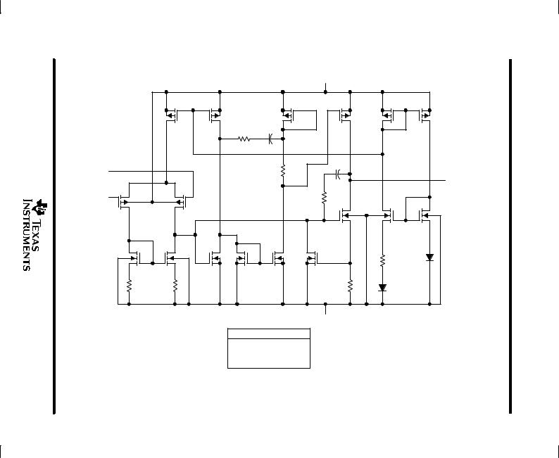
equivalent schematic |
|
|
|
|
|
|
|
|
|
|
|
|
VDD + |
|
|
|
Q3 |
Q6 |
|
Q9 |
Q12 |
Q14 |
Q16 |
|
|
|
R7 |
C2 |
|
|
|
|
|
|
|
|
|
|
|
IN + |
|
|
|
R6 |
|
|
|
|
|
|
|
|
C1 |
|
OUT |
|
|
|
|
|
|
|
|
IN ± |
|
|
|
|
R5 |
|
|
Q1 |
|
Q4 |
|
|
|
|
|
|
|
|
|
|
Q13 |
Q15 |
Q17 |
|
|
|
|
|
|
R2 |
D1 |
Q2 |
Q5 |
Q7 |
Q8 |
Q10 |
Q11 |
|
|
R3 |
R4 |
|
|
|
R1 |
D2 |
|
|
|
|
|
|
|
|
|
|
|
|
|
|
VDD ± / GND |
|
|
COMPONENT COUNT²
Transistors |
23 |
Diodes |
6 |
Resistors |
11 |
Capacitors |
2 |
²Includes both amplifiers and all ESD, bias, and trim circuitry
TLV2711Y TLV2711, RAIL-TO-RAIL LinCMOS Advanced AMPLIFIERS OPERATIONAL SINGLE MICROPOWER 1997 AUGUST ± SLOS196
TLV2711, TLV2711Y
Advanced LinCMOS RAIL-TO-RAIL
MICROPOWER SINGLE OPERATIONAL AMPLIFIERS
SLOS196 ± AUGUST 1997
absolute maximum ratings over operating free-air temperature range (unless otherwise noted)²
Supply voltage, VDD (see Note 1) . . . . . . . . . . . . . . . . . . . . . . . . . . . . . . . . . . . . . . . |
. . . . . . . . . . . . . . . . . . . . . 12 V |
Differential input voltage, VID (see Note 2) . . . . . . . . . . . . . . . . . . . . . . . . . . . . . . . |
. . . . . . . . . . . . . . . . . . . . ± VDD |
Input voltage range, VI (any input, see Note 1) . . . . . . . . . . . . . . . . . . . . . . . . . . . . |
. . . . . . . . . . . . ±0.3 V to VDD |
Input current, II (each input) . . . . . . . . . . . . . . . . . . . . . . . . . . . . . . . . . . . . . . . . . . . . |
. . . . . . . . . . . . . . . . . . . ± 5 mA |
Output current, IO . . . . . . . . . . . . . . . . . . . . . . . . . . . . . . . . . . . . . . . . . . . . . . . . . . . . . |
. . . . . . . . . . . . . . . . . . ± 50 mA |
Total current into VDD + . . . . . . . . . . . . . . . . . . . . . . . . . . . . . . . . . . . . . . . . . . . . . . . . |
. . . . . . . . . . . . . . . . . . ± 50 mA |
Total current out of VDD ± . . . . . . . . . . . . . . . . . . . . . . . . . . . . . . . . . . . . . . . . . . . . . . |
. . . . . . . . . . . . . . . . . . ± 50 mA |
Duration of short-circuit current (at or below) 25°C (see Note 3) . . . . . . . . . . . . . |
. . . . . . . . . . . . . . . . . unlimited |
Continuous total power dissipation . . . . . . . . . . . . . . . . . . . . . . . . . . . . . . . . . . . . . |
See Dissipation Rating Table |
Operating free-air temperature range, TA: TLV2711C . . . . . . . . . . . . . . . . . . . . . |
. . . . . . . . . . . . . . 0°C to 70°C |
TLV2711I . . . . . . . . . . . . . . . . . . . . . . |
. . . . . . . . . . . . ±40°C to 85°C |
Storage temperature range, Tstg . . . . . . . . . . . . . . . . . . . . . . . . . . . . . . . . . . . . . . . . |
. . . . . . . . . . . ±65°C to 150°C |
Lead temperature 1,6 mm (1/16 inch) from case for 10 seconds: DBV package |
. . . . . . . . . . . . . . . . . . 260°C |
²Stresses beyond those listed under ªabsolute maximum ratingsº may cause permanent damage to the device. These are stress ratings only, and functional operation of the device at these or any other conditions beyond those indicated under ªrecommended operating conditionsº is not
implied. Exposure to absolute-maximum-rated conditions for extended periods may affect device reliability. NOTES: 1. All voltage values, except differential voltages, are with respect to VDD ±.
2.Differential voltages are at the noninverting input with respect to the inverting input. Excessive current flows when input is brought below VDD ± ± 0.3 V.
3.The output may be shorted to either supply. Temperature and /or supply voltages must be limited to ensure that the maximum dissipation rating is not exceeded.
|
|
DISSIPATION RATING TABLE |
|
||
PACKAGE |
TA ≤ 25°C |
DERATING FACTOR |
TA = 70°C |
TA = 85°C |
|
POWER RATING |
ABOVE TA = 25°C |
POWER RATING |
POWER RATING |
||
|
|||||
DBV |
150 mW |
1.2 mW/°C |
96 mW |
78 mW |
|
|
|
|
|
|
|
recommended operating conditions
|
|
TLV2711C |
TLV2711I |
UNIT |
||
|
|
|
|
|
|
|
|
|
MIN |
MAX |
MIN |
MAX |
|
|
|
|
||||
|
|
|
|
|
|
|
Supply voltage, VDD (see Note 1) |
|
2.7 |
10 |
2.7 |
10 |
V |
Input voltage range, VI |
|
VDD ± |
VDD + ± 1.3 |
VDD ± |
VDD + ± 1.3 |
V |
Common-mode input voltage, VIC |
|
VDD ± |
VDD + ± 1.3 |
VDD ± |
VDD + ± 1.3 |
V |
Operating free-air temperature, TA |
|
0 |
70 |
± 40 |
85 |
°C |
NOTE 1: All voltage values, except differential voltages, are with respect to VDD ±. |
|
|
|
|
|
|
4 |
POST OFFICE BOX 655303 •DALLAS, TEXAS 75265 |
TLV2711, TLV2711Y
Advanced LinCMOS RAIL-TO-RAIL
MICROPOWER SINGLE OPERATIONAL AMPLIFIERS
SLOS196 ± AUGUST 1997
electrical characteristics at specified free-air temperature, VDD = 3 V (unless otherwise noted)
|
PARAMETER |
TEST CONDITIONS |
T ² |
TLV2711C |
|
|
TLV2711I |
|
UNIT |
||
|
|
|
|
|
|
|
|||||
|
|
|
|
|
|
|
|||||
|
|
|
|
A |
MIN |
TYP |
MAX |
MIN |
TYP |
MAX |
|
|
|
|
|
|
|
||||||
VIO |
Input offset voltage |
|
|
|
|
0.4 |
3 |
|
0.4 |
3 |
mV |
αVIO |
Temperature |
|
|
Full range |
|
|
|
|
|
|
μV/°C |
coefficient of input |
|
|
|
1 |
|
|
1 |
|
|||
|
|
|
|
|
|
|
|||||
|
offset voltage |
VDD ± = ± 1.5 V, |
VIC = 0, |
|
|
|
|
|
|
|
|
|
|
|
|
|
|
|
|
|
|
||
|
Input offset voltage |
|
|
|
|
|
|
|
|
||
|
VO = 0, |
RS = 50 Ω |
|
|
|
|
|
|
|
|
|
|
long-term drift |
25°C |
|
0.003 |
|
|
0.003 |
|
μV/mo |
||
|
|
|
|
|
|
|
|||||
|
(see Note 4) |
|
|
|
|
|
|
|
|
|
|
|
|
|
|
|
|
|
|
|
|
|
|
IIO |
Input offset current |
|
|
Full range |
|
0.5 |
150 |
|
0.5 |
150 |
pA |
IIB |
Input bias current |
|
|
Full range |
|
1 |
150 |
|
1 |
150 |
pA |
|
|
|
|
25°C |
0 |
± 0.3 |
|
0 |
± 0.3 |
|
|
|
|
|
|
to |
to |
|
to |
to |
|
|
|
VICR |
Common-mode input |
|VIO | ≤ 5 mV, |
RS = 50 Ω |
|
2 |
2.2 |
|
2 |
2.2 |
|
V |
voltage range |
|
0 |
|
|
0 |
|
|
||||
|
|
|
|
|
|
|
|
|
|||
|
|
|
|
|
|
|
|
|
|
||
|
|
|
|
Full range |
to |
|
|
to |
|
|
|
|
|
|
|
|
1.7 |
|
|
1.7 |
|
|
|
|
|
|
|
|
|
|
|
|
|
|
|
|
High-level output |
IOH = ± 100 μA |
|
25°C |
|
2.94 |
|
|
2.94 |
|
|
VOH |
|
|
25°C |
|
2.85 |
|
|
2.85 |
|
V |
|
voltage |
μ |
|
|
|
|
|
|||||
|
|
IOH = ±250 A |
|
Full range |
2.6 |
|
|
2.6 |
|
|
|
|
|
|
|
|
|
|
|
|
|||
|
|
|
|
|
|
|
|
|
|
|
|
|
Low-level output |
VIC = 1.5 V, |
IOL = 50 μA |
25°C |
|
15 |
|
|
15 |
|
|
VOL |
|
|
25°C |
|
150 |
|
|
150 |
|
mV |
|
voltage |
|
μ |
|
|
|
|
|||||
|
|
VIC = 1.5 V, |
IOL = 500 A |
Full range |
|
|
500 |
|
|
500 |
|
|
|
|
|
|
|
|
|
|
|||
|
|
|
|
|
|
|
|
|
|
|
|
|
Large-signal |
VIC = 1.5 V, |
RL = 10 kΩ³ |
25°C |
3 |
7 |
|
3 |
7 |
|
|
|
|
|
|
|
|
|
|
|
|||
AVD |
differential voltage |
Full range |
1 |
|
|
1 |
|
|
V/mV |
||
VO = 1 V to 2 V |
|
|
|
|
|
||||||
amplification |
RL = 1 MΩ³ |
25°C |
|
600 |
|
|
600 |
|
|
||
|
|
|
|
|
|
|
|||||
|
|
|
|
|
|
|
|
||||
ri(d) |
Differential input |
|
|
25°C |
|
1012 |
|
|
1012 |
|
Ω |
resistance |
|
|
|
|
|
|
|||||
|
|
|
|
|
|
|
|
|
|
|
|
|
|
|
|
|
|
|
|
|
|
|
|
ri(c) |
Common-mode |
|
|
25°C |
|
1012 |
|
|
1012 |
|
Ω |
input resistance |
|
|
|
|
|
|
|||||
|
|
|
|
|
|
|
|
|
|
|
|
|
|
|
|
|
|
|
|
|
|
|
|
ci(c) |
Common-mode |
f = 10 kHz, |
|
25°C |
|
5 |
|
|
5 |
|
pF |
input capacitance |
|
|
|
|
|
||||||
|
|
|
|
|
|
|
|
|
|
|
|
|
|
|
|
|
|
|
|
|
|
|
|
zo |
Closed-loop |
f = 7 kHz, |
AV = 1 |
25°C |
|
200 |
|
|
200 |
|
Ω |
output impedance |
|
|
|
|
|||||||
|
|
|
|
|
|||||||
|
|
|
|
|
|
|
|
|
|
|
|
|
|
|
|
|
|
|
|
|
|
|
|
CMRR |
Common-mode |
VIC = 0 to 1.7 V, |
VO = 1.5 V, |
25°C |
65 |
83 |
|
65 |
83 |
|
dB |
|
|
|
|
|
|
|
|||||
rejection ratio |
RS = 50 Ω |
|
Full range |
60 |
|
|
60 |
|
|
||
kSVR |
Supply voltage |
VDD = 2.7 V to 8 V, |
VIC = VDD /2 |
25°C |
80 |
95 |
|
80 |
95 |
|
dB |
rejection ratio |
|
|
|
|
|
|
|
||||
No load |
, |
Full range |
80 |
|
|
80 |
|
|
|||
|
( VDD / VIO) |
|
|
|
|
|
|||||
|
|
|
|
|
|
|
|
||||
IDD |
Supply current |
VO = 1.5 V, |
No load |
25°C |
|
11 |
25 |
|
11 |
25 |
μA |
|
|
|
|
|
|
|
|||||
Full range |
|
|
30 |
|
|
30 |
|||||
|
|
|
|
|
|
|
|
|
|||
|
|
|
|
|
|
|
|
|
|
|
|
² Full range for the TLV2711C is 0°C to 70°C. Full range for the TLV2711I is ± 40°C to 85°C. ³ Referenced to 1.5 V
NOTE 4: Typical values are based on the input offset voltage shift observed through 500 hours of operating life test at TA = 150°C extrapolated to TA = 25°C using the Arrhenius equation and assuming an activation energy of 0.96 eV.
POST OFFICE BOX 655303 •DALLAS, TEXAS 75265 |
5 |

TLV2711, TLV2711Y
Advanced LinCMOS RAIL-TO-RAIL
MICROPOWER SINGLE OPERATIONAL AMPLIFIERS
SLOS196 ± AUGUST 1997
operating characteristics at specified free-air temperature, VDD = 3 V (unless otherwise noted)
|
PARAMETER |
TEST CONDITIONS |
T ² |
TLV2711C |
TLV2711I |
|
UNIT |
||||
|
|
|
|
|
|||||||
|
|
|
|
|
|||||||
|
|
|
|
A |
MIN |
TYP MAX |
MIN TYP |
MAX |
|
|
|
|
|
|
|
|
|
|
|
||||
|
|
VO = 1.1 V to 1.9 V, |
RL = 10 kΩ³ , |
25°C |
0.01 |
0.025 |
0.01 0.025 |
|
|
|
|
SR |
Slew rate at unity gain |
|
|
|
|
|
V/μs |
||||
Full |
|
|
|
|
|||||||
|
|
CL = 100 pF³ |
|
0.005 |
|
0.005 |
|
|
|
|
|
|
|
|
|
range |
|
|
|
|
|
|
|
Vn |
Equivalent input noise |
f = 10 Hz |
|
25°C |
|
80 |
80 |
|
|
|
|
|
|
|
nV/√ Hz |
||||||||
voltage |
f = 1 kHz |
|
° |
|
22 |
22 |
|
||||
|
|
|
25 C |
|
|
|
|
|
|||
VN(PP) |
Peak-to-peak equivalent |
f = 0.1 Hz to 1 Hz |
|
25°C |
|
660 |
660 |
|
μV |
||
input noise voltage |
f = 0.1 Hz to 10 Hz |
|
° |
|
880 |
880 |
|
||||
|
|
|
25 C |
|
|
|
|
|
|||
|
Equivalent input noise |
|
|
25°C |
|
|
|
|
|
|
|
In |
|
|
|
0.6 |
0.6 |
|
fA /√ Hz |
||||
current |
|
|
|
|
|||||||
|
|
|
|
|
|
|
|
|
|
|
|
|
|
|
|
|
|
|
|
|
|
||
|
Gain-bandwidth product |
f = 10 kHz, |
RL = 10 kΩ³ , |
25°C |
|
56 |
56 |
|
kHz |
||
|
|
CL = 100 pF³ |
|
|
|
|
|
|
|
|
|
BOM |
Maximum output-swing |
VO(PP) = 1 V, |
AV = 1, |
25°C |
|
7 |
7 |
|
kHz |
||
bandwidth |
RL = 10 kΩ³ , |
CL = 100 pF³ |
|
|
|||||||
|
|
|
|
|
|
|
|
|
|||
φm |
Phase margin at |
|
|
25°C |
|
56° |
56° |
|
|
|
|
unity gain |
RL = 10 kΩ³ , |
CL = 100 pF³ |
|
|
|
|
|
||||
|
|
|
|
|
|
|
|
|
|||
|
Gain margin |
|
|
25°C |
|
20 |
20 |
|
dB |
||
|
|
|
|
|
|
|
|
|
|
|
|
² |
Full range is ± 40°C to 85°C. |
³ |
Referenced to 1.5 V |
6 |
POST OFFICE BOX 655303 •DALLAS, TEXAS 75265 |
TLV2711, TLV2711Y
Advanced LinCMOS RAIL-TO-RAIL
MICROPOWER SINGLE OPERATIONAL AMPLIFIERS
SLOS196 ± AUGUST 1997
electrical characteristics at specified free-air temperature, VDD = 5 V (unless otherwise noted)
|
PARAMETER |
TEST CONDITIONS |
T ² |
TLV2711C |
|
|
TLV2711I |
|
UNIT |
||
|
|
|
|
|
|
|
|||||
|
|
|
|
|
|
|
|||||
|
|
|
|
A |
MIN |
TYP |
MAX |
MIN |
TYP |
MAX |
|
|
|
|
|
|
|
||||||
VIO |
Input offset voltage |
|
|
|
|
0.45 |
3 |
|
0.45 |
3 |
mV |
|
Temperature |
|
|
Full range |
|
|
|
|
|
|
|
αVIO |
coefficient of input |
|
|
|
0.5 |
|
|
0.5 |
|
μV/°C |
|
|
|
|
|
|
|
|
|||||
|
offset voltage |
|
|
|
|
|
|
|
|
|
|
|
|
|
|
|
|
|
|
|
|
|
|
|
Input offset voltage |
VDD ± = ± 2.5 V, |
VIC = 0, |
|
|
|
|
|
|
|
|
|
long-term drift |
° |
|
0.003 |
|
|
0.003 |
|
μ |
||
|
VO = 0, |
RS = 50 Ω |
25 C |
|
|
|
|
V/mo |
|||
|
(see Note 4) |
|
|
|
|
|
|
|
|
||
IIO |
Input offset current |
|
|
25°C |
|
0.5 |
|
|
0.5 |
|
pA |
|
|
|
|
|
|
|
|
|
|||
|
|
Full range |
|
|
150 |
|
|
150 |
|||
|
|
|
|
|
|
|
|
|
|||
|
|
|
|
|
|
|
|
|
|
|
|
IIB |
Input bias current |
|
|
25°C |
|
1 |
|
|
1 |
|
pA |
|
|
|
|
|
|
|
|
|
|||
|
|
Full range |
|
|
150 |
|
|
150 |
|||
|
|
|
|
|
|
|
|
|
|||
|
|
|
|
|
|
|
|
|
|
|
|
|
|
|
|
|
0 |
± 0.3 |
|
0 |
± 0.3 |
|
|
|
|
|
|
25°C |
to |
to |
|
to |
to |
|
|
VICR |
Common-mode input |
|VIO | ≤ 5 mV |
RS = 50 Ω |
|
4 |
4.2 |
|
4 |
4.2 |
|
V |
voltage range |
|
0 |
|
|
0 |
|
|
||||
|
|
|
|
|
|
|
|
|
|
||
|
|
|
|
Full range |
to |
|
|
to |
|
|
|
|
|
|
|
|
3.5 |
|
|
3.5 |
|
|
|
|
|
|
|
|
|
|
|
|
|
|
|
|
High-level output |
IOH = ± 100 μA |
|
25°C |
|
4.95 |
|
|
4.95 |
|
|
VOH |
|
|
25°C |
|
4.875 |
|
|
4.875 |
|
V |
|
voltage |
IOH = ±250 μA |
|
|
|
|
|
|||||
|
|
Full range |
4.6 |
|
|
4.6 |
|
|
|
||
|
|
|
|
|
|
|
|
|
|||
|
|
|
|
|
|
|
|
|
|
|
|
|
Low-level output |
VIC = 2.5 V, |
IOL = 50 μA |
25°C |
|
12 |
|
|
12 |
|
|
VOL |
|
|
25°C |
|
120 |
|
|
120 |
|
mV |
|
voltage |
VIC = 2.5 V, |
IOL = 500 μA |
|
|
|
|
|||||
|
Full range |
|
|
500 |
|
|
500 |
|
|||
|
|
|
|
|
|
|
|
|
|||
|
|
|
|
|
|
|
|
|
|
|
|
|
Large-signal |
VIC = 2.5 V, |
RL = 10 kΩ³ |
25°C |
6 |
12 |
|
6 |
12 |
|
|
|
|
|
|
|
|
|
|
|
|||
AVD |
Full range |
3 |
|
|
3 |
|
|
V/mV |
|||
differential |
VO = 1 V to 4 V |
|
|
|
|
|
|||||
|
voltage amplification |
RL = 1 MΩ³ |
25°C |
|
800 |
|
|
800 |
|
|
|
|
|
|
|
|
|
|
|||||
|
|
|
|
|
|
|
|
||||
ri(d) |
Differential input |
|
|
25°C |
|
1012 |
|
|
1012 |
|
Ω |
resistance |
|
|
|
|
|
|
|||||
|
|
|
|
|
|
|
|
|
|
|
|
|
|
|
|
|
|
|
|
|
|
|
|
ri(c) |
Common-mode |
|
|
25°C |
|
1012 |
|
|
1012 |
|
Ω |
input resistance |
|
|
|
|
|
|
|||||
|
|
|
|
|
|
|
|
|
|
|
|
|
|
|
|
|
|
|
|
|
|
|
|
ci(c) |
Common-mode |
f = 10 kHz, |
|
25°C |
|
5 |
|
|
5 |
|
pF |
input capacitance |
|
|
|
|
|
||||||
|
|
|
|
|
|
|
|
|
|
|
|
|
|
|
|
|
|
|
|
|
|
|
|
zo |
Closed-loop |
f = 7 kHz, |
AV = 1 |
25°C |
|
200 |
|
|
200 |
|
Ω |
output impedance |
|
|
|
|
|||||||
|
|
|
|
|
|||||||
|
|
|
|
|
|
|
|
|
|
|
|
|
|
|
|
|
|
|
|
|
|
|
|
CMRR |
Common-mode |
VIC = 0 to 2.7 V, |
VO = 2.5 V, |
25°C |
70 |
83 |
|
70 |
83 |
|
dB |
rejection ratio |
RS = 50 Ω |
|
Full range |
70 |
|
|
70 |
|
|
||
|
Supply voltage |
VDD = 4.4 V to 8 V, |
VIC = VDD /2, |
25°C |
80 |
95 |
|
80 |
95 |
|
|
kSVR |
rejection ratio |
|
|
|
|
|
|
|
dB |
||
No load |
|
Full range |
80 |
|
|
80 |
|
|
|||
|
( VDD / VIO) |
|
|
|
|
|
|
|
|||
IDD |
Supply current |
VO = 2.5 V, |
No load |
25°C |
|
13 |
25 |
|
13 |
25 |
μA |
|
|
|
|
|
|
|
|||||
Full range |
|
|
30 |
|
|
30 |
|||||
|
|
|
|
|
|
|
|
|
|||
|
|
|
|
|
|
|
|
|
|
|
|
² Full range for the TLV2711C is 0°C to 70°C. Full range for the TLV2711I is ± 40°C to 85°C. ³ Referenced to 1.5 V
NOTE 5: Typical values are based on the input offset voltage shift observed through 500 hours of operating life test at TA = 150°C extrapolated to TA = 25°C using the Arrhenius equation and assuming an activation energy of 0.96 eV.
POST OFFICE BOX 655303 •DALLAS, TEXAS 75265 |
7 |
TLV2711, TLV2711Y
Advanced LinCMOS RAIL-TO-RAIL
MICROPOWER SINGLE OPERATIONAL AMPLIFIERS
SLOS196 ± AUGUST 1997
operating characteristics at specified free-air temperature, VDD = 5 V (unless otherwise noted)
|
PARAMETER |
TEST CONDITIONS |
T ² |
TLV2711C |
TLV2711I |
|
UNIT |
||||
|
|
|
|
|
|||||||
|
|
|
|
|
|||||||
|
|
|
|
A |
MIN |
TYP MAX |
MIN TYP |
MAX |
|
|
|
|
|
|
|
|
|
|
|
||||
|
|
VO = 1.5 V to 3.5 V, |
RL = 10 kΩ³ , |
25°C |
0.01 |
0.025 |
0.01 0.025 |
|
|
|
|
SR |
Slew rate at unity gain |
|
|
|
|
|
V/μs |
||||
Full |
|
|
|
|
|||||||
|
|
CL = 100 pF³ |
|
0.005 |
|
0.005 |
|
|
|
|
|
|
|
|
|
range |
|
|
|
|
|
|
|
Vn |
Equivalent input noise |
f = 10 Hz |
|
25°C |
|
72 |
72 |
|
|
|
|
|
|
|
nV/√ Hz |
||||||||
voltage |
f = 1 kHz |
|
° |
|
21 |
21 |
|
||||
|
|
|
25 C |
|
|
|
|
|
|||
VN(PP) |
Peak-to-peak equivalent |
f = 0.1 Hz to 1 Hz |
|
25°C |
|
600 |
600 |
|
μV |
||
input noise voltage |
f = 0.1 Hz to 10 Hz |
|
° |
|
800 |
800 |
|
||||
|
|
|
25 C |
|
|
|
|
|
|||
|
Equivalent input noise |
|
|
25°C |
|
|
|
|
|
|
|
In |
|
|
|
0.6 |
0.6 |
|
fA /√ Hz |
||||
current |
|
|
|
|
|||||||
|
|
|
|
|
|
|
|
|
|
|
|
|
|
|
|
|
|
|
|
|
|
||
|
Gain-bandwidth product |
f = 10 kHz, |
RL = 10 kΩ³ , |
25°C |
|
65 |
65 |
|
kHz |
||
|
|
CL = 100 pF³ |
|
|
|
|
|
|
|
|
|
BOM |
Maximum output-swing |
VO(PP) = 2 V, |
AV = 1, |
25°C |
|
7 |
7 |
|
kHz |
||
bandwidth |
RL = 10 kΩ³ , |
CL = 100 pF³ |
|
|
|||||||
|
|
|
|
|
|
|
|
|
|||
φm |
Phase margin at |
|
|
25°C |
|
60° |
60° |
|
|
|
|
unity gain |
RL = 10 kΩ³ , |
CL = 100 pF³ |
|
|
|
|
|
||||
|
|
|
|
|
|
|
|
|
|||
|
Gain margin |
|
|
25°C |
|
22 |
22 |
|
dB |
||
|
|
|
|
|
|
|
|
|
|
|
|
² |
Full range is ± 40°C to 85°C. |
³ |
Referenced to 1.5 V |
electrical characteristics at VDD = 3 V, TA = 25°C (unless otherwise noted)
|
|
PARAMETER |
TEST CONDITIONS |
|
|
TLV2711Y |
|
UNIT |
|
|
|
|
|
|
|
|
|
||||
|
|
|
MIN |
TYP |
MAX |
|
||||
|
|
|
|
|
|
|
|
|||
|
|
|
|
|
|
|
|
|
|
|
|
VIO |
Input offset voltage |
VDD ± = ± 1.5 V, |
VO = 0, |
VIC = 0, |
|
0.47 |
|
mV |
|
|
IIO |
Input offset current |
|
0.5 |
|
pA |
|
|||
|
RS = 50 Ω |
|
|
|
|
|
||||
|
IIB |
Input bias current |
|
|
|
1 |
|
pA |
|
|
|
|
|
|
|
|
|
||||
|
|
|
|
|
|
|
± 0.3 |
|
|
|
|
VICR |
Common-mode input voltage range |
| VIO | ≤ 5 mV, |
RS = 50 Ω |
|
|
to |
|
V |
|
|
|
|
|
|
|
|
2.2 |
|
|
|
|
|
|
|
|
|
|
|
|
|
|
|
VOH |
High-level output voltage |
IOH = ±100 μA |
|
|
|
2.94 |
|
V |
|
|
IOH = ± 200 μA |
|
|
|
2.85 |
|
|
|||
|
|
|
|
|
|
|
|
|
||
|
VOL |
Low-level output voltage |
VIC = 0, |
IOL = 50 μA |
|
|
15 |
|
mV |
|
|
VIC = 0, |
IOL = 500 μA |
|
|
150 |
|
|
|||
|
|
|
|
|
|
|
|
|||
|
AVD |
Large-signal differential |
VIC = 1.5 V, |
VO = 1 V to 2 V |
RL = 10 kΩ² |
|
7 |
|
V/mV |
|
|
voltage amplification |
RL = 1 MΩ² |
|
600 |
|
|
||||
|
|
|
|
|
|
|
|
|||
|
ri(d) |
Differential input resistance |
|
|
|
|
1012 |
|
Ω |
|
|
ri(c) |
Common-mode input resistance |
|
|
|
|
1012 |
|
Ω |
|
|
ci(c) |
Common-mode input capacitance |
f = 10 kHz |
|
|
|
5 |
|
pF |
|
|
zo |
Closed-loop output impedance |
f = 7 kHz, |
AV = 1 |
|
|
200 |
|
Ω |
|
|
CMRR |
Common-mode rejection ratio |
VIC = 0 to 1.7 V, |
VO = 1.5 V, |
RS = 50 Ω |
|
83 |
|
dB |
|
|
kSVR |
Supply voltage rejection ratio |
VDD = 2.7 V to 8 V, |
VIC = VDD/2, |
No load |
|
95 |
|
dB |
|
|
( VDD / VIO) |
|
|
|
||||||
|
|
|
|
|
|
|
|
|
|
|
|
IDD |
Supply current |
VO = 1.5 V, |
No load |
|
|
11 |
|
μA |
|
|
² Referenced to 1.5 V |
|
|
|
|
|
|
|
|
|
|
|
|
|
|
|
|
|
|
|
|
|
|
|
|
|
|
|
|
|
|
|
8 |
POST OFFICE BOX 655303 •DALLAS, TEXAS 75265 |
TLV2711, TLV2711Y
Advanced LinCMOS RAIL-TO-RAIL
MICROPOWER SINGLE OPERATIONAL AMPLIFIERS
SLOS196 ± AUGUST 1997
electrical characteristics at VDD = 5 V, TA = 25°C (unless otherwise noted)
|
PARAMETER |
TEST CONDITIONS |
|
|
TLV2711Y |
|
UNIT |
|
|
|
|
|
|
||||
|
|
MIN |
TYP |
MAX |
||||
|
|
|
|
|
|
|||
|
|
|
|
|
|
|
|
|
VIO |
Input offset voltage |
VDD ± = ± 2.5 V, |
VIC = 0, |
VO = 0, |
|
0.45 |
|
mV |
IIO |
Input offset current |
|
0.5 |
|
pA |
|||
RS = 50 Ω |
|
|
|
|
||||
IIB |
Input bias current |
|
|
|
1 |
|
pA |
|
|
|
|
|
|
||||
|
|
|
|
|
|
± 0.3 |
|
|
VICR |
Common-mode input voltage range |
| VIO | ≤ 5 mV, |
RS = 50 Ω |
|
|
to |
|
V |
|
|
|
|
|
|
4.2 |
|
|
|
|
|
|
|
|
|
|
|
VOH |
High-level output voltage |
IOH = ± 100 μA |
|
|
|
4.95 |
|
V |
IOH = ± 250 μA |
|
|
|
4.875 |
|
|||
|
|
|
|
|
|
|
||
VOL |
Low-level output voltage |
VIC = 2.5 V, |
IOL = 50 μA |
|
|
12 |
|
mV |
VIC = 2.5 V, |
IOL = 500 μA |
|
|
120 |
|
|||
|
|
|
|
|
|
|||
AVD |
Large-signal differential |
VIC = 2.5 V, |
VO = 1 V to 4 V |
RL = 10 kΩ² |
|
12 |
|
V/mV |
voltage amplification |
RL = 1 MΩ² |
|
800 |
|
||||
|
|
|
|
|
|
|||
ri(d) |
Differential input resistance |
|
|
|
|
1012 |
|
Ω |
ri(c) |
Common-mode input resistance |
|
|
|
|
1012 |
|
Ω |
ci(c) |
Common-mode input capacitance |
f = 10 kHz |
|
|
|
5 |
|
pF |
zo |
Closed-loop output impedance |
f = 7 kHz, |
AV = 1 |
|
|
200 |
|
Ω |
CMRR |
Common-mode rejection ratio |
VIC = 0 to 2.7 V, |
VO = 2.5 V, |
RS = 50 Ω |
|
83 |
|
dB |
kSVR |
Supply voltage rejection ratio |
VDD = 4.4 V to 8 V, |
VIC = VDD/2, |
No load |
|
95 |
|
dB |
( VDD / VIO) |
|
|
||||||
|
|
|
|
|
|
|
|
|
IDD |
Supply current |
VO = 2.5 V, |
No load |
|
|
13 |
|
μA |
² Referenced to 1.5 V |
|
|
|
|
|
|
|
|
POST OFFICE BOX 655303 •DALLAS, TEXAS 75265 |
9 |
 Loading...