


Texas Instruments TLV2444IPWR, TLV2444IPW, TLV2444IDR, TLV2444ID, TLV2444CPWR Datasheet
...TLV2442, TLV2442A, TLV2444, TLV2444A Advanced LinCMOS RAIL-TO-RAIL OUTPUT
WIDE-INPUT-VOLTAGE OPERATIONAL AMPLIFIERS
SLOS169F ± NOVEMBER 1996 ± REVISED NOVEMBER 1999
DOutput Swing Includes Both Supply Rails
DExtended Common-Mode Input Voltage Range . . . 0 V to 4.25 V (Min) at 5-V Single Supply
DNo Phase Inversion
DLow Noise . . . 16 nV/√ Hz Typ at f = 1 kHz
DLow Input Offset Voltage
950 µV Max at TA = 25°C (TLV244xA)
DLow Input Bias Current . . . 1 pA Typ
description
The TLV244x and TLV244xA are low-voltage operational amplifiers from Texas Instruments. The common-mode input voltage range of these devices has been extended over typical standard CMOS amplifiers, making them suitable for a wide range of applications. In addition, these devices do not phase invert when the common-mode input is driven to the supply rails. This satisfies most design requirements without paying a premium for rail-to-rail input performance. They also exhibit rail-to-rail output performance for increased dynamic range in singleor split-supply applications. This family is fully characterized at 3-V and 5-V supplies and is optimized for low-voltage operation. Both devices offer comparable ac performance while having lower noise, input offset voltage, and power dissipation than existing CMOS operational amplifiers. The TLV244x has increased output drive over previous rail-to-rail operational amplifiers and can drive 600-Ω loads for telecommunications applications.
D600-Ω Output Drive
DHigh-Gain Bandwidth . . . 1.8 MHz Typ
DLow Supply Current . . . 750 µA Per Channel
Typ
DMacromodel Included
DAvailable in Q-Temp Automotive
HighRel Automotive Applications Configuration Control / Print Support Qualification to Automotive Standards
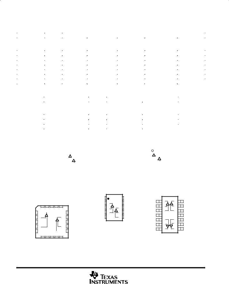
HIGH-LEVEL OUTPUT VOLTAGE vs
HIGH-LEVEL OUTPUT CURRENT
|
3 |
|
|
|
|
|
|
|
|
|
|
|
|
VDD = 3 V |
|
± V |
2.5 |
|
|
|
|
|
|
|
|
|
|
|
|
|
|
Voltage |
2 |
|
|
|
|
|
|
|
|
|
|
|
TA = ± 40°C |
|
|
-Level Output |
|
|
|
|
|
|
|
1.5 |
|
|
|
|
|
|
|
1 |
|
|
|
|
|
|
|
High |
|
|
|
|
|
|
|
|
|
TA = 125°C |
|
|
|
||
± |
|
|
|
|
|
|
|
OH |
0.5 |
|
|
TA = 85°C |
TA = 25°C |
|
|
V |
|
|
|
|
|
|
|
|
0 |
|
|
|
|
|
|
|
0 |
2 |
4 |
6 |
8 |
10 |
12 |
|
|
IOH ± High-Level Output Current ± mA |
|
||||
Figure 1
The other members in the TLV244x family are the low-power, TLV243x, and micro-power, TLV2422, versions.
The TLV244x, exhibiting high input impedance and low noise, is excellent for small-signal conditioning for high-impedance sources, such as piezoelectric transducers. Because of the micropower dissipation levels and low-voltage operation, these devices work well in hand-held monitoring and remote-sensing applications. In addition, the rail-to-rail output feature with singleor split-supplies makes this family a great choice when interfacing with analog-to-digital converters (ADCs). For precision applications, the TLV244xA is available with a maximum input offset voltage of 950 µV.
If the design requires single operational amplifiers, see the TI TLV2211/21/31. This is a family of rail-to-rail output operational amplifiers in the SOT-23 package. Their small size and low power consumption make them ideal for high density, battery-powered equipment.
Please be aware that an important notice concerning availability, standard warranty, and use in critical applications of Texas Instruments semiconductor products and disclaimers thereto appears at the end of this data sheet.
Advanced LinCMOS is a trademark of Texas Instruments Incorporated.
PRODUCTION DATA information is current as of publication date. Products conform to specifications per the terms of Texas Instruments standard warranty. Production processing does not necessarily include testing of all parameters.
Copyright 1999, Texas Instruments Incorporated
On products compliant to MIL-PRF-38535, all parameters are tested unless otherwise noted. On all other products, production processing does not necessarily include testing of all parameters.
POST OFFICE BOX 655303 •DALLAS, TEXAS 75265 |
1 |
TLV2442, TLV2442A, TLV2444, TLV2444A |
|
|
|
|
|
|||
Advanced LinCMOS |
RAIL-TO-RAIL OUTPUT |
|
|
|
|
|
||
WIDE-INPUT-VOLTAGE OPERATIONAL AMPLIFIERS |
|
|
|
|||||
SLOS169F ± NOVEMBER 1996 ± REVISED NOVEMBER 1999 |
|
|
|
|
|
|||
|
|
|
|
|
|
|
|
|
|
|
|
TLV2442 AVAILABLE OPTIONS |
|
|
|
||
|
|
|
|
|
|
|
|
|
|
|
|
|
PACKAGED DEVICES |
|
|
|
|
|
VIOmax |
|
|
|
|
|
|
|
TA |
SMALL |
CHIP CARRIER |
CERAMIC DIP |
|
TSSOP |
CERAMIC FLAT |
|
|
AT 25°C |
OUTLINE |
|
PACK |
|
||||
|
(FK) |
(JG) |
|
(PW) |
|
|||
|
|
(D) |
|
(U) |
|
|||
|
|
|
|
|
|
|
||
|
|
|
|
|
|
|
|
|
0°C to 70°C |
2.5 mV |
TLV2442CD |
Ð |
Ð |
|
TLV2442CPW |
Ð |
|
|
|
|
|
|
|
|
|
|
±40°C to 85°C |
950 V |
TLV2442AID |
Ð |
Ð |
|
TLV2442AIPW |
Ð |
|
2.5 mV |
TLV2442ID |
Ð |
Ð |
|
Ð |
Ð |
|
|
|
|
|
||||||
|
|
|
|
|
|
|
|
|
±40°C to 125°C |
950 V |
TLV2442AQD |
Ð |
Ð |
|
Ð |
Ð |
|
2.5 mV |
TLV2442QD |
Ð |
Ð |
|
Ð |
Ð |
|
|
|
|
|
||||||
|
|
|
|
|
|
|
|
|
±55°C to 125°C |
950 V |
Ð |
TLV2442AMFK |
TLV2442AMJG |
|
Ð |
TLV2442AMU |
|
2.5 mV |
Ð |
TLV2442MFK |
TLV2442MJG |
|
Ð |
TLV2442MU |
|
|
|
|
|
||||||
|
|
|
|
|
|
|
|
|
The D and PW packages are available taped and reeled. Add R suffix to device type (e.g., TLV2442CDR).
TLV2444 AVAILABLE OPTIONS
|
|
PACKAGED DEVICES |
||
|
VIOmax |
|
|
|
TA |
SMALL |
TSSOP |
||
AT 25°C |
OUTLINE |
|||
|
(PW) |
|||
|
|
(D) |
||
|
|
|
||
|
|
|
|
|
0°C to 70°C |
2.5 mV |
TLV2444CD |
TLV2444CPW |
|
|
|
|
|
|
±40°C to 125°C |
950 V |
TLV2444AID |
TLV2444AIPW |
|
2.5 mV |
TLV2444ID |
TLV2444IPW |
||
|
||||
The D and PW packages are available taped and reeled. Add R suffix to device type (e.g., TLV2444CDR).
TLV2442
D OR JG PACKAGE
(TOP VIEW)
1OUT |
|
|
|
1 |
|
|
|
8 |
|
|
VDD + |
|||||
|
|
|
|
|
|
|
|
|||||||||
|
|
|
|
|
|
|
|
|||||||||
1IN ± |
|
|
2 |
|
|
|
|
|
|
7 |
|
|
2OUT |
|||
1IN + |
|
|
|
3 |
|
|
|
|
|
|
|
|
6 |
|
|
2IN ± |
|
|
|
|
|
|
|
|
|
||||||||
VDD ±/GND |
|
|
|
4 |
|
|
|
|
|
|
|
|
5 |
|
|
2IN + |
|
|
|
|
|
|
|
|
|
|
|
|
|||||
|
|
|
|
|
|
|
|
|
|
|
|
|
|
|
|
|
TLV2442
FK PACKAGE (TOP VIEW)
TLV2442
PW PACKAGE (TOP VIEW)
1OUT |
|
|
1 |
|
|
|
8 |
|
|
VDD + |
||||
|
|
|
|
|
|
|
||||||||
1IN± |
|
|
2 |
|
|
|
|
|
7 |
|
|
2OUT |
||
1IN + |
|
|
3 |
|
|
|
|
|
|
|
6 |
|
|
2IN ± |
|
|
|
|
|
|
|
|
|
|
|
||||
|
|
|
|
|
|
|
|
|||||||
|
|
|
|
|
|
|
||||||||
VDD ±/ GND |
|
|
4 |
|
|
|
|
|
|
|
5 |
|
|
2IN + |
|
|
|
|
|
|
|
||||||||
TLV2442 |
TLV2444 |
U PACKAGE |
D OR PW PACKAGE |
(TOP VIEW) |
(TOP VIEW) |
|
|
NC |
1OUT |
NC |
DD+ |
NC |
|
1OUT |
2 |
9 |
VDD + |
|
|
|
|
|
|
V |
|
|
|
|
|
|||||||||
|
|
|
|
|
|
|
NC |
1 |
10 |
NC |
1OUT |
1 |
14 |
4OUT |
|
|
|
|
|
|
|
|
|
|
|
|
|||||
|
|
|
|
|
|
|
1IN ± |
3 |
8 |
2OUT |
1IN ± |
2 |
13 |
4IN ± |
|
|
3 |
2 |
1 |
20 19 |
|
1IN+ |
3 |
12 |
4IN+ |
||||||
NC |
NC |
1IN + |
4 |
7 |
2IN ± |
||||||||||
4 |
|
|
|
18 |
VDD+ |
4 |
11 |
VDD±/GND |
|||||||
1IN ± |
5 |
|
|
|
17 |
2OUT |
VDD ±/GND |
5 |
6 |
2IN + |
|||||
|
|
|
|
|
|||||||||||
NC |
6 |
|
|
|
16 |
NC |
|
|
|
|
2IN+ |
5 |
10 |
3IN+ |
|
|
|
|
|
|
|
|
2IN ± |
6 |
9 |
3IN ± |
|||||
1IN + |
7 |
|
|
|
15 |
2IN ± |
|
|
|
|
|||||
|
|
|
|
|
|
|
2OUT |
7 |
8 |
3OUT |
|||||
NC |
8 |
|
|
|
14 |
NC |
|
|
|
|
|||||
|
|
|
|
|
|
|
|
|
|
|
|||||
|
9 |
10 11 12 13 |
|
|
|
|
|
|
|
|
|
||||
|
NC |
/GND |
NC |
2IN+ |
NC |
|
|
|
|
|
|
|
|
|
|
|
|
DD± |
|
|
|
|
|
|
|
|
|
|
|
|
|
|
|
V |
|
|
|
|
|
|
|
|
|
|
|
|
|
NC ± No internal connection |
|
|
|
|
|
|
|
|
|
||||||
2 |
POST OFFICE BOX 655303 •DALLAS, TEXAS 75265 |

75265 TEXAS DALLAS, •655303 BOX OFFICE POST
3
equivalent schematic (each amplifier) |
|
|
|
|
|
|
||
Q22 |
|
|
|
|
Q29 |
Q31 |
Q34 |
Q36 |
|
|
|
|
|
|
VB3 |
|
|
|
|
|
Q26 |
|
|
|
|
|
|
|
Q24 |
|
|
|
Q32 |
|
VB2 |
VB1 |
|
|
|
|
|
|
|
|
|
|
Q25 |
Q27 |
|
|
Q33 |
Q35 |
VB4 |
|
|
|
|
|
|
|
|
|
Q23 |
|
|
|
|
Q30 |
|
|
|
|
|
|
|
|
|
|
R10 |
Q37 |
|
R9 |
|
|
|
D1 |
|
|
|
|
|
|
|
|
|
|
||
|
Q3 |
R3 |
R4 |
|
Q13 |
Q15 |
|
R7 |
|
|
|
|
|
|
|
||
IN± |
Q4 |
Q6 |
Q8 |
Q10 |
|
|
Q18 |
|
Q1 |
|
|
|
|
|
|
|
|
IN+ |
|
|
|
|
|
|
|
Q20 |
|
|
|
|
|
|
|
|
|
|
|
|
|
|
|
|
R5 |
C2 |
|
|
Q7 |
Q9 |
|
|
|
|
|
|
|
|
|
|
|
|
||
|
|
|
|
|
C1 |
|
|
|
|
|
VB3 |
|
Q11 |
|
Q16 |
R6 |
C3 |
|
|
|
|
|
||||
|
|
|
|
|
|
|
|
|
VB2 |
|
|
|
|
|
|
|
|
Q2 |
|
Q5 |
|
|
|
Q14 |
|
Q21 |
|
|
|
|
|
|
|||
|
|
|
|
|
|
|
|
|
|
|
|
|
Q12 |
|
Q17 |
Q19 |
|
R1 |
|
R2 |
|
|
|
|
|
|
|
|
|
|
VB4 |
|
|
|
R8 |
|
|
|
|
|
|
|
|
|
COMPONENT
COUNT
Transistors 69
Diodes 5
Resistors 26
Capacitors 6
VDD+
VDD±/GND
OUT
TLV2444A TLV2444, TLV2442A, TLV2442, OUTPUT RAIL-TO-RAIL LinCMOS Advanced AMPLIFIERS OPERATIONAL VOLTAGE-INPUT-WIDE 1999 NOVEMBER REVISED ± 1996 NOVEMBER ± SLOS169F

TLV2442, TLV2442A, TLV2444, TLV2444A
Advanced LinCMOS RAIL-TO-RAIL OUTPUT
WIDE-INPUT-VOLTAGE OPERATIONAL AMPLIFIERS
SLOS169F ± NOVEMBER 1996 ± REVISED NOVEMBER 1999
absolute maximum ratings over operating free-air temperature range (unless otherwise noted)²
Supply voltage, VDD (see Note 1) . . . . . . . . . . . . . . . . . . . . . . . . . . . . . . . . . . . . . . . |
. . . . . . . . . . . . . . . . . . . . . 12 V |
Differential input voltage, VID (see Note 2) . . . . . . . . . . . . . . . . . . . . . . . . . . . . . . . |
. . . . . . . . . . . . . . . . . . . . ± VDD |
Input voltage, VI (any input, see Note 1) . . . . . . . . . . . . . . . . . . . . . . . . . . . . . . . . . |
. . . . . . . . . . . . ±0.3 V to VDD |
Input current, II (any input) . . . . . . . . . . . . . . . . . . . . . . . . . . . . . . . . . . . . . . . . . . . . . |
. . . . . . . . . . . . . . . . . . . ± 5 mA |
Output current, IO . . . . . . . . . . . . . . . . . . . . . . . . . . . . . . . . . . . . . . . . . . . . . . . . . . . . . |
. . . . . . . . . . . . . . . . . . ± 50 mA |
Total current into VDD + . . . . . . . . . . . . . . . . . . . . . . . . . . . . . . . . . . . . . . . . . . . . . . . . |
. . . . . . . . . . . . . . . . . . ± 50 mA |
Total current out of VDD ± . . . . . . . . . . . . . . . . . . . . . . . . . . . . . . . . . . . . . . . . . . . . . . |
. . . . . . . . . . . . . . . . . . ± 50 mA |
Duration of short-circuit current at (or below) 25°C (see Note 3) . . . . . . . . . . . . . |
. . . . . . . . . . . . . . . . . unlimited |
Continuous total dissipation . . . . . . . . . . . . . . . . . . . . . . . . . . . . . . . . . . . . . . . . . . . |
See Dissipation Rating Table |
Operating free-air temperature range, TA: C suffix . . . . . . . . . . . . . . . . . . . . . . . . . |
. . . . . . . . . . . . . . 0°C to 70°C |
I suffix (dual) . . . . . . . . . . . . . . . . . . . . |
. . . . . . . . . . . . ±40°C to 85°C |
I suffix (quad) . . . . . . . . . . . . . . . . . . . |
. . . . . . . . . . . ±40°C to 125°C |
Q suffix . . . . . . . . . . . . . . . . . . . . . . . . . |
. . . . . . . . . . . ±40°C to 125°C |
M suffix . . . . . . . . . . . . . . . . . . . . . . . . . |
. . . . . . . . . . . ±55°C to 125°C |
Storage temperature range, Tstg . . . . . . . . . . . . . . . . . . . . . . . . . . . . . . . . . . . . . . . . |
. . . . . . . . . . . ±65°C to 150°C |
Lead temperature 1,6 mm (1/16 inch) from case for 10 seconds . . . . . . . . . . . . |
. . . . . . . . . . . . . . . . . . . 260°C |
²Stresses beyond those listed under ªabsolute maximum ratingsº may cause permanent damage to the device. These are stress ratings only, and functional operation of the device at these or any other conditions beyond those indicated under ªrecommended operating conditionsº is not
implied. Exposure to absolute-maximum-rated conditions for extended periods may affect device reliability.
NOTES: 1. All voltage values, except differential voltages, are with respect to the midpoint between VDD+ and VDD ±.
2. Differential voltages are at IN+ with respect to IN ±. Excessive current will flow if input is brought below VDD ± ± 0.3 V.
3.The output may be shorted to either supply. Temperature and/or supply voltages must be limited to ensure that the maximum dissipation rating is not exceeded.
DISSIPATION RATING TABLE
PACKAGE |
TA ≤ 25°C |
DERATING FACTOR |
TA = 70°C |
TA = 85°C |
TA = 125°C |
|
POWER RATING |
ABOVE TA = 25°C |
POWER RATING |
POWER RATING |
POWER RATING |
||
|
||||||
D (8) |
725 mW |
5.8 mW/°C |
464 mW |
377 mW |
145 mW |
|
D (14) |
1022 mW |
7.6 mW/°C |
900 mW |
777 mW |
450 mW |
|
FK |
1375 mW |
11.0 mW/°C |
880 mW |
715 mW |
275 mW |
|
JG |
1050 mW |
8.4 mW/°C |
672 mW |
546 mW |
210 mW |
|
PW (8) |
525 mW |
4.2 mW/°C |
336 mW |
273 mW |
105 mW |
|
PW (14) |
720 mW |
5.6 mW/°C |
634 mW |
547 mW |
317 mW |
|
U |
675 mW |
5.4 mW/°C |
432 mW |
350 mW |
135 mW |
|
|
|
|
|
|
|
recommended operating conditions
|
C SUFFIX |
I SUFFIX |
Q SUFFIX |
M SUFFIX |
UNIT |
|||||
|
|
|
|
|
|
|
|
|
||
|
MIN |
MAX |
MIN |
MAX |
MIN |
MAX |
MIN |
MAX |
||
|
|
|||||||||
|
|
|
|
|
|
|
|
|
|
|
Supply voltage, VDD |
2.7 |
10 |
2.7 |
10 |
2.7 |
10 |
2.7 |
10 |
V |
|
Input voltage range, VI |
VDD ± |
VDD + ± 1 |
VDD ± |
VDD + ± 1 |
VDD ± |
VDD + ± 1.3 |
VDD ± |
VDD + ± 1.3 |
V |
|
Common-mode input voltage, |
VDD ± |
VDD + ± 1 |
VDD ± |
VDD + ± 1 |
VDD ± + 2 |
VDD + ± 1.3 |
VDD ± + 2 |
VDD + ± 1.3 |
V |
|
VIC |
||||||||||
|
|
|
|
|
|
|
|
|
||
Operating free-air temperature, |
0 |
70 |
± 40 |
125 |
± 40 |
125 |
± 55 |
125 |
°C |
|
TA |
||||||||||
|
|
|
|
|
|
|
|
|
||
4 |
POST OFFICE BOX 655303 •DALLAS, TEXAS 75265 |
TLV2442, TLV2442A, TLV2444, TLV2444A
Advanced LinCMOS RAIL-TO-RAIL OUTPUT
WIDE-INPUT-VOLTAGE OPERATIONAL AMPLIFIERS
SLOS169F ± NOVEMBER 1996 ± REVISED NOVEMBER 1999
electrical characteristics at specified free-air temperature, VDD = 3 V (unless otherwise noted)
|
PARAMETER |
TEST CONDITIONS |
T ² |
|
TLV2442 |
|
UNIT |
||
|
|
|
|
||||||
|
|
|
|
||||||
|
|
|
|
|
A |
MIN |
TYP |
MAX |
|
|
|
|
|
|
|
|
|||
|
|
|
|
TLV244xC |
25°C |
|
300 |
2000 |
|
|
|
|
|
TLV244xI |
Full range |
|
|
2500 |
|
|
|
|
|
|
|
|
|
|
|
VIO |
Input offset voltage |
|
|
TLV244xAI |
25°C |
|
300 |
950 |
µV |
|
|
|
|
|
|
||||
|
|
Full range |
|
|
1500 |
||||
|
|
|
|
|
|
|
|
||
|
|
|
|
|
|
|
|
|
|
|
|
|
|
TLV2442AQ |
25°C |
|
300 |
950 |
|
|
|
|
|
TLV2442AM |
Full range |
|
|
1600 |
|
|
|
|
|
|
|
|
|
|
|
αVIO |
Temperature coefficient of input |
|
|
|
25°C |
|
2 |
|
µV/°C |
offset voltage |
|
|
|
to 85°C |
|
|
|||
|
VIC = 1.5 V, |
|
|
|
|
|
|
||
|
|
|
|
|
|
|
|
|
|
|
Input offset voltage long-term drift |
|
|
|
|
|
|
|
|
|
VO = 1.5 V, |
|
|
25°C |
|
0.002 |
|
µV/mo |
|
|
(see Note 4) |
|
|
|
|
||||
|
RS = 50 Ω |
|
|
|
|
|
|
|
|
|
|
|
|
|
|
|
|
|
|
IIO |
Input offset current |
|
|
|
25°C |
|
0.5 |
|
pA |
|
|
|
|
|
|
|
|||
|
|
|
Full range |
|
|
150 |
|||
|
|
|
|
|
|
|
|
||
|
|
|
|
|
|
|
|
|
|
|
|
|
|
|
25°C |
|
1 |
|
|
|
|
|
|
|
|
|
|
|
|
|
|
|
|
|
±40°C to |
|
|
150 |
|
|
|
|
|
|
85°C |
|
|
|
|
IIB |
Input bias current |
|
|
|
|
|
|
pA |
|
|
|
|
|
|
|
|
|||
|
|
|
125°C |
|
|
350 |
|||
|
|
|
|
|
|
|
|
||
|
|
|
|
TLV2442Q/AQ |
Full range |
|
|
260 |
|
|
|
|
|
TLV2442M/AM |
|
|
|
||
|
|
|
|
|
|
|
|
|
|
|
|
|
|
|
|
|
|
|
|
|
|
|
|
|
|
0 |
±0.25 |
|
|
|
|
|
|
|
25°C |
to |
to |
|
|
|
|
|
|
|
|
2.25 |
2.5 |
|
|
|
|
|
|
|
|
|
|
|
|
|
|
|
|
|
|
0 |
|
|
|
|
|
|
|
|
Full range |
to |
|
|
|
VICR |
Common-mode input voltage |
|VIO| ≤ 5 mV, |
RS = 50 Ω |
|
2 |
|
|
V |
|
range |
25°C to |
0 |
±0.25 |
|
|||||
|
|
|
|
|
|
||||
|
|
|
|
|
to |
to |
|
|
|
|
|
|
|
|
±55°C |
|
|
||
|
|
|
|
|
2.25 |
2.5 |
|
|
|
|
|
|
|
|
|
|
|
||
|
|
|
|
|
|
|
|
|
|
|
|
|
|
|
|
0 |
|
|
|
|
|
|
|
|
125°C |
to |
|
|
|
|
|
|
|
|
|
2 |
|
|
|
|
|
|
|
|
|
|
|
|
|
|
|
IO = ± 100 µA |
|
|
25°C |
|
2.98 |
|
|
VOH |
High-level output voltage |
IO = ±3 mA |
|
|
25°C |
|
2.5 |
|
V |
|
|
|
|
Full range |
2.25 |
|
|
|
|
|
|
|
|
|
|
|
|
||
|
|
|
|
|
|
|
|
|
|
|
|
VIC = 1.5 V, |
IO = 100 µA |
25°C |
|
0.02 |
|
|
|
VOL |
Low-level output voltage |
VIC = 1.5 V, |
IO = 3 mA |
25°C |
|
0.63 |
|
V |
|
|
|
Full range |
|
|
1 |
|
|||
|
|
|
|
|
|
|
|
||
|
|
|
|
|
|
|
|
|
|
|
Large-signal differential |
|
RL = 600 Ω |
25°C |
0.7 |
1 |
|
|
|
AVD |
VO = 1 V to 2 V |
Full range |
0.4 |
|
|
V/mV |
|||
voltage amplification |
|
|
|
|
|||||
|
|
RL = 1 MΩ |
25°C |
|
750 |
|
|
||
|
|
|
|
|
|
||||
rid |
Differential input resistance |
|
|
|
25°C |
|
1000 |
|
GΩ |
ri |
Common-mode input resistance |
|
|
|
25°C |
|
1000 |
|
GΩ |
ci |
Common-mode input capacitance |
f = 10 kHz |
|
|
25°C |
|
8 |
|
pF |
zo |
Closed-loop output impedance |
f = 1 MHz, |
AV = 10 |
25°C |
|
130 |
|
Ω |
|
²Full range for the C suffix is 0°C to 70°C. Full range for the dual I suffix is ± 40°C to 85°C. Full range for the quad I suffix is ± 40°C to 125°C. Full range for the Q suffix is ± 40°C to 125°C. Full range for the M suffix is ± 55°C to 125°C.
NOTE 4: Typical values are based on the input offset voltage shift observed through 168 hours of operating life test at TA = 150°C extrapolated to TA = 25°C using the Arrhenius equation and assuming an activation energy of 0.96 eV.
POST OFFICE BOX 655303 •DALLAS, TEXAS 75265 |
5 |
TLV2442, TLV2442A, TLV2444, TLV2444A
Advanced LinCMOS RAIL-TO-RAIL OUTPUT
WIDE-INPUT-VOLTAGE OPERATIONAL AMPLIFIERS
SLOS169F ± NOVEMBER 1996 ± REVISED NOVEMBER 1999
electrical characteristics at specified free-air temperature, VDD = 3 V (unless otherwise noted) (continued)
|
PARAMETER |
TEST CONDITIONS |
T ² |
|
TLV2442 |
|
UNIT |
|
|
|
|
|
|||||
|
|
|
|
|||||
|
|
|
|
A |
MIN |
TYP |
MAX |
|
|
|
|
|
|
|
|||
|
|
VIC = 0 to 2.25 V, |
|
25°C |
65 |
75 |
|
|
|
|
|
|
|
|
|
|
|
|
|
|
Full range |
55 |
|
|
|
|
CMRR |
Common-mode rejection ratio |
VO = 1.5 V, |
|
|
|
dB |
||
|
|
|
|
|
||||
TLV2442Q/AQ |
|
|
|
|
||||
|
|
RS = 50 Ω |
Full range |
50 |
|
|
|
|
|
|
TLV2442M/AM |
|
|
|
|||
|
|
|
|
|
|
|
|
|
|
|
|
|
|
|
|
|
|
kSVR |
Supply-voltage rejection ratio |
VDD = 2.7 V to 8 V, VIC = VDD/2, |
25°C |
80 |
95 |
|
dB |
|
( VDD ± / VIO) |
No load |
|
Full range |
80 |
|
|
||
|
|
|
|
|
||||
IDD |
Supply current (per channel) |
VO = 1.5 V, |
|
25°C |
|
725 |
1100 |
µA |
No load |
|
Full range |
|
|
1100 |
|||
|
|
|
|
|
|
|||
|
|
|
|
|
|
|
|
|
²Full range for the C suffix is 0°C to 70°C. Full range for the dual I suffix is ± 40°C to 85°C. Full range for the quad I suffix is ± 40°C to 125°C. Full range for the Q suffix is ± 40°C to 125°C. Full range for the M suffix is ± 55°C to 125°C.
operating characteristics at specified free-air temperature, VDD = 3 V
|
PARAMETER |
TEST CONDITIONS |
T ² |
|
TLV244x |
|
UNIT |
|||||||
|
|
|
|
|||||||||||
|
|
|
|
|||||||||||
|
|
|
|
|
|
A |
MIN |
TYP |
MAX |
|
|
|
|
|
|
|
|
|
|
|
|
|
|
|
|
|
|||
|
|
|
|
|
|
25°C |
0.65 |
1.3 |
|
|
|
|
|
|
|
|
VO = 1 V to 2 V, |
|
Full |
0.65 |
|
|
V/µs |
||||||
SR |
Slew rate at unity gain |
RL = 600 Ω, |
|
|
|
range |
|
|
||||||
|
|
|
|
|
|
|||||||||
|
|
CL = 100 pF |
|
TLV2442Q/AQ |
Full |
0.4 |
|
|
|
|
|
|
|
|
|
|
|
|
TLV2442M/AM |
range |
|
|
|
|
|
|
|
||
|
|
|
|
|
|
|
|
|
|
|
|
|||
|
|
|
|
|
|
|
|
|
|
|
|
|
|
|
Vn |
Equivalent input noise voltage |
f = 10 Hz |
|
|
|
25°C |
|
170 |
|
nV/√ |
|
|
|
|
|
|
|
|
|
|
|
|
Hz |
|
|||||
f = 1 kHz |
|
|
|
25°C |
|
18 |
|
|
||||||
|
|
|
|
|
|
|
|
|
|
|
|
|||
|
|
|
|
|
|
|
|
|
|
|
|
|
||
VN(PP) |
Peak-to-peak equivalent input noise voltage |
f = 0.1 Hz to 1 Hz |
|
25°C |
|
2.6 |
|
µV |
||||||
|
|
|
|
|
|
|
|
|||||||
f = 0.1 Hz to 10 Hz |
|
25°C |
|
5.1 |
|
|||||||||
|
|
|
|
|
|
|
|
|
|
|||||
|
|
|
|
|
|
|
|
|
|
|
|
|
||
|
|
|
|
|
|
25°C |
|
|
|
|
||||
In |
Equivalent input noise current |
|
|
|
|
|
0.6 |
|
fA/√ |
Hz |
|
|||
|
|
VO = 0.5 V to 2.5 V, |
AV = 1 |
|
|
0.08% |
|
|
|
|
|
|
||
|
|
|
25°C |
|
|
|
|
|
|
|
|
|||
THD + N |
Total harmonic distortion plus noise |
RL = 600 Ω, |
|
|
AV = 10 |
|
0.3% |
|
|
|
|
|
|
|
|
|
f = 1 kHz |
|
|
AV = 100 |
|
|
2% |
|
|
|
|
|
|
|
|
|
|
|
|
|
|
|
|
|
|
|
||
|
Gain-bandwidth product |
f =10 kHz, |
|
RL = 600 Ω, |
25°C |
|
1.75 |
|
MHz |
|||||
|
|
CL = 100 pF |
|
|
|
|
|
|
|
|
|
|
|
|
BOM |
Maximum output-swing bandwidth |
VO(PP) = 1 V, |
|
RL = 600 Ω, |
25°C |
|
0.9 |
|
MHz |
|||||
AV = 1, |
|
CL = 100 pF |
|
|
||||||||||
|
|
|
|
|
|
|
|
|
|
|
|
|||
|
|
AV = ±1, |
to 2.3 V, |
To 0.1% |
|
|
1.5 |
|
|
|
|
|
|
|
ts |
Settling time |
Step = ± 2.3 V |
|
25°C |
|
|
|
µs |
||||||
RL = 600 Ω, |
|
|
To 0.01% |
|
3.2 |
|
||||||||
|
|
|
|
|
|
|
|
|
|
|
|
|||
|
|
CL = 100 pF |
|
|
|
|
|
|
|
|
|
|
||
|
|
|
|
|
|
|
|
|
|
|
|
|
|
|
φm |
Phase margin at unity gain |
RL = 600 Ω, |
|
CL = 100 pF |
25°C |
|
65° |
|
|
|
|
|
|
|
|
Gain margin |
|
25°C |
|
9 |
|
dB |
|||||||
|
|
|
|
|
|
|
||||||||
|
|
|
|
|
|
|
|
|
|
|
|
|
|
|
²Full range for the C suffix is 0°C to 70°C. Full range for the dual I suffix is ± 40°C to 85°C. Full range for the quad I suffix is ± 40°C to 125°C. Full range for the Q suffix is ± 40°C to 125°C. Full range for the M suffix is ± 55°C to 125°C.
6 |
POST OFFICE BOX 655303 •DALLAS, TEXAS 75265 |

TLV2442, TLV2442A, TLV2444, TLV2444A
Advanced LinCMOS RAIL-TO-RAIL OUTPUT
WIDE-INPUT-VOLTAGE OPERATIONAL AMPLIFIERS
SLOS169F ± NOVEMBER 1996 ± REVISED NOVEMBER 1999
electrical characteristics at specified free-air temperature, VDD = 5 V (unless otherwise noted)
|
PARAMETER |
TEST CONDITIONS |
T ² |
|
TLV244x |
|
UNIT |
||
|
|
|
|
||||||
|
|
|
|
||||||
|
|
|
|
|
A |
MIN |
TYP |
MAX |
|
|
|
|
|
|
|
|
|||
|
|
|
|
TLV244xC |
25°C |
|
300 |
2000 |
|
|
|
|
|
TLV244xI |
Full range |
|
|
2500 |
|
|
|
|
|
|
|
|
|
|
|
VIO |
Input offset voltage |
|
|
TLV244xA |
25°C |
|
300 |
950 |
µV |
|
|
|
|
|
|
||||
|
|
Full range |
|
|
1500 |
||||
|
|
|
|
|
|
|
|
||
|
|
|
|
|
|
|
|
|
|
|
|
|
|
TLV2442AQ |
25°C |
|
300 |
950 |
|
|
|
|
|
TLV2442AM |
Full range |
|
|
1600 |
|
|
|
|
|
|
|
|
|
|
|
αVIO |
Temperature coefficient of input |
|
|
|
25°C |
|
2 |
|
µV/°C |
offset voltage |
|
|
|
to 85°C |
|
|
|||
|
|
|
|
|
|
|
|
||
|
|
|
|
|
|
|
|
|
|
|
Input offset voltage long-term |
VDD ± = ± 2.5 V, |
VIC = 0, |
|
|
|
|
|
|
|
drift |
25°C |
|
0.002 |
|
µV/mo |
|||
|
VO = 0, |
RS = 50 Ω |
|
|
|||||
|
(see Note 4) |
|
|
|
|
|
|||
|
|
|
|
|
|
|
|
|
|
|
|
|
|
|
|
|
|
|
|
IIO |
Input offset current |
|
|
|
25°C |
|
0.5 |
|
pA |
|
|
|
Full range |
|
|
150 |
|||
|
|
|
|
|
|
|
|
||
|
|
|
|
|
|
|
|
|
|
|
|
|
|
|
25°C |
|
1 |
|
|
|
|
|
|
|
±40°C to |
|
|
150 |
|
|
|
|
|
|
85°C |
|
|
|
|
IIB |
Input bias current |
|
|
|
|
|
|
pA |
|
|
|
|
|
|
|
|
|||
|
|
|
125°C |
|
|
350 |
|||
|
|
|
|
|
|
|
|
||
|
|
|
|
|
|
|
|
|
|
|
|
|
|
TLV2442Q/AQ |
Full range |
|
|
260 |
|
|
|
|
|
TLV2442M/AM |
|
|
|
||
|
|
|
|
|
|
|
|
|
|
|
|
|
|
|
|
|
|
|
|
|
|
|
|
|
|
0 |
±0.25 |
|
|
|
|
|
|
|
25°C |
to |
to |
|
|
VICR |
Common-mode input voltage |
|VIO| ≤ 5 mV, |
RS = 50 Ω |
|
4.25 |
4.5 |
|
V |
|
range |
|
0 |
|
|
|||||
|
|
|
|
|
|
|
|
||
|
|
|
|
|
Full range |
to |
|
|
|
|
|
|
|
|
|
4 |
|
|
|
|
|
|
|
|
|
|
|
|
|
|
|
IOH = ± 100 µA |
|
|
25°C |
|
4.97 |
|
|
VOH |
High-level output voltage |
IOH = ±5 mA |
|
|
25°C |
4 |
4.35 |
|
V |
|
|
|
|
Full range |
4 |
|
|
|
|
|
|
|
|
|
|
|
|
||
|
|
|
|
|
|
|
|
|
|
|
|
VIC = 2.5 V, |
IOL = 100 µA |
25°C |
|
0.01 |
|
|
|
VOL |
Low-level output voltage |
VIC = 2.5 V, |
IOL = 5 mA |
25°C |
|
0.8 |
|
V |
|
|
|
Full range |
|
|
1.25 |
|
|||
|
|
|
|
|
|
|
|
||
|
|
|
|
|
|
|
|
|
|
|
Large-signal differential |
VIC = 2.5 V, |
RL = 600 Ω³ |
25°C |
0.9 |
1.3 |
|
|
|
|
|
|
|
|
|
||||
AVD |
Full range |
0.5 |
|
|
V/mV |
||||
voltage amplification |
VO = 1 V to 4 V |
|
|
|
|
||||
RL = 1 MΩ³ |
25°C |
|
950 |
|
|
||||
|
|
|
|
|
|
||||
rid |
Differential input resistance |
|
|
|
25°C |
|
1000 |
|
GΩ |
ri |
Common-mode input resistance |
|
|
|
25°C |
|
1000 |
|
GΩ |
ci |
Common-mode input |
f = 10 kHz |
|
|
25°C |
|
8 |
|
pF |
capacitance |
|
|
|
|
|||||
|
|
|
|
|
|
|
|
|
|
|
|
|
|
|
|
|
|
|
|
zo |
Closed-loop output impedance |
f = 1 MHz, |
AV = 10 |
25°C |
|
140 |
|
Ω |
|
CMRR |
Common-mode rejection ratio |
VIC = 0 to 4.25 V, |
VO = 2.5 V, |
25°C |
70 |
75 |
|
dB |
|
RS = 50 Ω |
|
|
Full range |
70 |
|
|
|||
|
|
|
|
|
|
|
|||
² |
Full range for the C suffix is 0°C to 70°C. Full range for the dual I suffix is ± 40°C to 85°C. Full range for the quad I suffix is ± 40°C to 125°C. Full |
|
range for the Q suffix is ± 40°C to 125°C. Full range for the M suffix is ± 55°C to 125°C. |
³ Referenced to 2.5 V |
|
NOTE 4: Typical values are based on the input offset voltage shift observed through 168 hours of operating life test at TA = 150°C extrapolated to TA = 25°C using the Arrhenius equation and assuming an activation energy of 0.96 eV.
POST OFFICE BOX 655303 •DALLAS, TEXAS 75265 |
7 |
TLV2442, TLV2442A, TLV2444, TLV2444A
Advanced LinCMOS RAIL-TO-RAIL OUTPUT
WIDE-INPUT-VOLTAGE OPERATIONAL AMPLIFIERS
SLOS169F ± NOVEMBER 1996 ± REVISED NOVEMBER 1999
electrical characteristics at specified free-air temperature, VDD = 5 V (unless otherwise noted) (continued)
|
PARAMETER |
|
|
TEST CONDITIONS |
T ² |
|
TLV244x |
|
UNIT |
|
|
|
|
|
|
|
|||||
|
|
|
|
|
|
|||||
|
|
|
|
|
|
A |
MIN |
TYP |
MAX |
|
|
|
|
|
|
|
|
|
|||
kSVR |
Supply-voltage rejection ratio ( |
VDD / |
VIO) |
VDD = 4.4 V to 8 V, |
|
25°C |
80 |
95 |
|
dB |
VIC = VDD /2, |
No load |
Full range |
80 |
|
|
|||||
|
|
|
|
|
|
|
||||
IDD |
Supply current (per channel) |
|
|
VO = 2.5 V, |
No load |
25°C |
|
750 |
1100 |
µA |
|
|
|
|
|
|
|||||
|
|
Full range |
|
|
1100 |
|||||
|
|
|
|
|
|
|
|
|
||
|
|
|
|
|
|
|
|
|
|
|
²Full range for the C suffix is 0°C to 70°C. Full range for the dual I suffix is ± 40°C to 85°C. Full range for the quad I suffix is ± 40°C to 125°C. Full range for the Q suffix is ± 40°C to 125°C. Full range for the M suffix is ± 55°C to 125°C.
operating characteristics at specified free-air temperature, VDD = 5 V
|
PARAMETER |
TEST CONDITIONS |
T ² |
|
TLV244x |
|
UNIT |
|||||||
|
|
|
|
|||||||||||
|
|
|
|
|||||||||||
|
|
|
|
|
|
A |
MIN |
TYP |
MAX |
|
|
|
|
|
|
|
|
|
|
|
|
|
|
|
|
|
|||
|
|
VO = 0.5 V to 2.5 V, |
|
|
25°C |
0.75 |
1.4 |
|
|
|
|
|
|
|
|
|
|
|
Full range |
0.75 |
|
|
|
|
|
|
|
||
SR |
Slew rate at unity gain |
RL = 600 Ω³ , |
|
|
|
|
|
V/ s |
||||||
|
|
|
|
|
|
|
||||||||
|
|
CL = 100 pF³ |
|
|
TLV2442Q/AQ |
Full range |
0.5 |
|
|
|
|
|
|
|
|
|
|
|
|
TLV2442M/AM |
|
|
|
|
|
|
|
|
|
Vn |
Equivalent input noise voltage |
f = 10 Hz |
|
|
|
25°C |
|
130 |
|
nV/√ |
|
|
|
|
|
|
|
|
|
|
|
|
Hz |
|
|||||
f = 1 kHz |
|
|
|
25°C |
|
16 |
|
|
||||||
|
|
|
|
|
|
|
|
|
|
|
|
|||
|
|
|
|
|
|
|
|
|
|
|
|
|
|
|
VN(PP) |
Peak-to-peak equivalent input noise |
f = 0.1 Hz to 1 Hz |
|
|
25°C |
|
1.8 |
|
µV |
|||||
voltage |
f = 0.1 Hz to 10 Hz |
|
|
25°C |
|
3.6 |
|
|||||||
|
|
|
|
|
|
|
|
|
|
|||||
|
|
|
|
|
|
|
|
|
|
|
|
|
||
|
|
|
|
|
|
25°C |
|
|
|
|
||||
In |
Equivalent input noise current |
|
|
|
|
|
0.6 |
|
fA/√ |
Hz |
|
|||
|
|
VO = 1.5 V to 3.5 V, |
|
AV = 1 |
|
|
0.017% |
|
|
|
|
|
|
|
THD + N |
Total harmonic distortion plus noise |
f = 1 kHz, |
|
|
AV = 10 |
25°C |
|
0.17% |
|
|
|
|
|
|
|
|
RL = 600 Ω³ |
|
|
|
|
|
|
|
|
|
|
|
|
|
|
|
|
AV = 100 |
|
|
1.5% |
|
|
|
|
|
|
|
|
Gain-bandwidth product |
f =10 kHz, |
RL = 600 Ω³ , |
25°C |
|
1.81 |
|
MHz |
||||||
|
|
CL = 100 pF³ |
|
|
|
|
|
|
|
|
|
|
|
|
BOM |
Maximum output-swing bandwidth |
VO(PP) = 2 V, |
AV |
= 1, |
25°C |
|
0.5 |
|
MHz |
|||||
RL = 600 Ω³ , |
CL |
= 100 pF³ |
|
|
||||||||||
|
|
|
|
|
|
|
|
|
|
|
||||
|
|
AV = ± 1, |
|
|
To 0.1% |
|
|
1.5 |
|
|
|
|
|
|
ts |
Settling time |
Step = 0.5 V to 2.5 V, |
|
25°C |
|
|
|
µs |
||||||
RL = 600 Ω³ , |
|
|
To 0.01% |
|
2.6 |
|
||||||||
|
|
CL = 100 pF³ |
|
|
|
|
|
|
|
|
|
|
||
|
|
|
|
|
|
|
|
|
|
|
|
|
|
|
φm |
Phase margin at unity gain |
RL = 600 Ω³ , |
CL |
= 100 pF³ |
25°C |
|
68° |
|
|
|
|
|
|
|
|
Gain margin |
25°C |
|
8 |
|
dB |
||||||||
|
|
|
|
|
|
|
||||||||
² Full range for the C suffix is 0°C to 70°C. Full range for the dual I suffix is ± 40°C to 85°C. Full range for the quad I suffix is ± 40°C to 125°C. Full range for the Q suffix is ± 40°C to 125°C. Full range for the M suffix is ± 55°C to 125°C.
³ Referenced to 2.5 V
8 |
POST OFFICE BOX 655303 •DALLAS, TEXAS 75265 |

TLV2442, TLV2442A, TLV2444, TLV2444A
Advanced LinCMOS RAIL-TO-RAIL OUTPUT
WIDE-INPUT-VOLTAGE OPERATIONAL AMPLIFIERS
SLOS169F ± NOVEMBER 1996 ± REVISED NOVEMBER 1999
TYPICAL CHARACTERISTICS
Table of Graphs²
|
|
|
FIGURE |
||
|
|
|
|
|
|
VIO |
Input offset voltage |
Distribution |
2, |
3 |
|
vs Common-mode voltage |
4, |
5 |
|||
|
|
||||
|
|
|
|
|
|
αVIO |
Input offset voltage temperature coefficient |
Distribution |
6, |
7 |
|
IIB /IIO |
Input bias and input offset currents |
vs Free-air temperature |
8 |
|
|
VOH |
High-level output voltage |
vs High-level output current |
9, 10 |
||
VOL |
Low-level output voltage |
vs Low-level output current |
11, 12 |
||
VO(PP) |
Maximum peak-to-peak output voltage |
vs Frequency |
13 |
||
IOS |
Short-circuit output current |
vs Supply voltage |
14 |
||
vs Free-air temperature |
15 |
||||
|
|
||||
|
|
|
|
|
|
VO |
Output voltage |
vs Differential Input voltage |
16, |
17 |
|
AVD |
Differential voltage amplification |
vs Load resistance |
18 |
||
AVD |
Large-signal differential voltage amplification |
vs Frequency |
19, |
20 |
|
vs Free-air temperature |
21, |
22 |
|||
|
|
||||
|
|
|
|
|
|
zo |
Output impedance |
vs Frequency |
23, |
24 |
|
CMRR |
Common-mode rejection ratio |
vs Frequency |
25 |
||
vs Free-air temperature |
26 |
||||
|
|
||||
|
|
|
|
|
|
kSVR |
Supply-voltage rejection ratio |
vs Frequency |
27, |
28 |
|
vs Free-air temperature |
29 |
||||
|
|
||||
|
|
|
|
||
IDD |
Supply current |
vs Supply voltage |
30 |
||
SR |
Slew rate |
vs Load capacitance |
31 |
||
vs Free-air temperature |
32 |
||||
|
|
||||
|
|
|
|
|
|
|
Inverting large-signal pulse response |
|
33, |
34 |
|
|
|
|
|
|
|
VO |
Voltage-follower large-signal pulse response |
|
35, |
36 |
|
|
|
|
|
||
Inverting small-signal pulse response |
|
37, |
38 |
||
|
|
||||
|
|
|
|
|
|
|
Voltage-follower small-signal pulse response |
|
39, |
40 |
|
|
|
|
|
|
|
Vn |
Equivalent input noise voltage |
vs Frequency |
41, |
42 |
|
|
Noise voltage |
Over a 10-second period |
43 |
||
|
|
|
|
|
|
THD + N |
Total harmonic distortion plus noise |
vs Frequency |
44, |
45 |
|
|
|
|
|
||
|
Gain-bandwidth product |
vs Free-air temperature |
46 |
||
|
vs Supply voltage |
47 |
|||
|
|
||||
|
|
|
|
|
|
φm |
Phase margin |
vs Frequency |
19, |
20 |
|
vs Load capacitance |
48 |
||||
|
|
||||
|
|
|
|
||
|
Gain margin |
vs Load capacitance |
49 |
||
|
|
|
|
||
B1 |
Unity-gain bandwidth |
vs Load capacitance |
50 |
||
² For all graphs where VDD = 5 V, all loads are referenced to 2.5 V.
POST OFFICE BOX 655303 •DALLAS, TEXAS 75265 |
9 |
 Loading...