


Texas Instruments TLV2545IDGKR, TLV2545IDR, TLV2545IDGK, TLV2545ID, TLV2545CDGKR Datasheet
...TLV2541, TLV2542, TLV2545 2.7 V TO 5.5 V, LOW POWER, 12-BIT, 200 KSPS, SERIAL ANALOG-TO-DIGITAL CONVERTERS WITH AUTOPOWER DOWN
SLAS245 ±MARCH 2000
D |
Maximum Throughput . . . 200 KSPS |
|
D Built-In Conversion Clock |
|
|
D INL/DNL: ±1 LSB Max, SINAD: 72 dB, |
D |
|
|
||
|
fi = 20 kHz, SFDR: 85 dB, fi = 20 kHz |
D |
D SPI/DSP-Compatible Serial Interfaces With |
|
|
|
SCLK up to 20 MHz |
|
D Single Supply 2.7 Vdc to 5.5 Vdc |
|
|
D Rail-to-Rail Analog Input With 500 kHz BW |
D |
|
|
Three Options Available: |
|
D |
|
|
± TLV2541 ± Single Channel Input
± TLV2542 ± Dual Channels With
Autosweep
±TLV2545 ± Single Channel With Pseudo-Differential Input
Optimized DSP Mode ± Requires FS Only
Low Power With Autopower Down
±Operating Current : 1 mA at 2.7 V, 1.5 mA
at 5 V
Autopower Down: 2 A at 2.7 V, 5 A at 5 V
Small 8-Pin MSOP and SOIC Packages
PACKAGE TOP VIEW |
TLV2542 |
TLV2545 |
TLV2541 |
|
|
|
|
|
SDO |
|
|
|
|
SDO |
|
|
|
|
SDO |
|
CS |
1 |
8 |
CS/FS |
1 |
8 |
CS/FS |
1 |
8 |
||||||
VREF |
2 |
7 |
FS |
VREF |
2 |
7 |
SCLK |
VREF |
2 |
7 |
SCLK |
||||
GND |
3 |
6 |
VDD |
GND |
3 |
6 |
VDD |
GND |
3 |
6 |
VDD |
||||
AIN |
4 |
5 |
SCLK |
AIN0 |
4 |
5 |
AIN1 |
AIN(+) |
4 |
5 |
AIN(±) |
||||
|
|
|
|
|
|
|
|
|
|
|
|
|
|
|
|
description
The TLV2541/2542/2545 are a family of high performance, 12-bit, low power, miniature 3.6 s, CMOS analog-to-digital converters (ADC). The TLV254x family operates from a single 2.7 V to 5.5 V. Devices are available with single, dual, or single pseudo-differential inputs. The TLV2541 has a 3-state output chip select (CS), serial output clock (SCLK), and serial data output (SDO) that provides a direct 3-wire interface to the serial port of most popular host microprocessors (SPI interface). When interfaced with a DSP, a frame sync signal (FS) is used to indicate the start of a serial data frame. The TLV2542/45 have a shared CS/FS terminal.
TLV2541/2/5 are designed to operate with very low power consumption. The power saving feature is further enhanced with an autopower-down mode. This product family features a high-speed serial link to modern host processors with SCLK up to 20 MHz. TLV254x family uses the built in oscillator as conversion clock, providing a 3.6 s conversion time.
AVAILABLE OPTIONS
|
PACKAGED DEVICES |
|
TA |
|
|
8-MSOP |
8-SOIC |
|
|
(DGK) |
(D) |
|
|
|
|
TLV2541CDGK |
|
0°C to 70°C |
|
|
TLV2542CDGK |
|
|
|
|
|
|
TLV2545CDGK |
|
|
|
|
|
TLV2541IDGK |
TLV2541ID |
± 40°C to 85°C |
|
|
TLV2542IDGK |
TLV2542ID |
|
|
|
|
|
TLV2545IDGK |
TLV2545ID |
Please be aware that an important notice concerning availability, standard warranty, and use in critical applications of Texas Instruments semiconductor products and disclaimers thereto appears at the end of this data sheet.
PRODUCTION DATA information is current as of publication date. Products conform to specifications per the terms of Texas Instruments standard warranty. Production processing does not necessarily include testing of all parameters.
Copyright 2000, Texas Instruments Incorporated
POST OFFICE BOX 655303 •DALLAS, TEXAS 75265 |
1 |
TLV2541, TLV2542, TLV2545
2.7 V TO 5.5 V, LOW POWER, 12-BIT, 200 KSPS,
SERIAL ANALOG-TO-DIGITAL CONVERTERS WITH AUTOPOWER DOWN
SLAS245 ±MARCH 2000
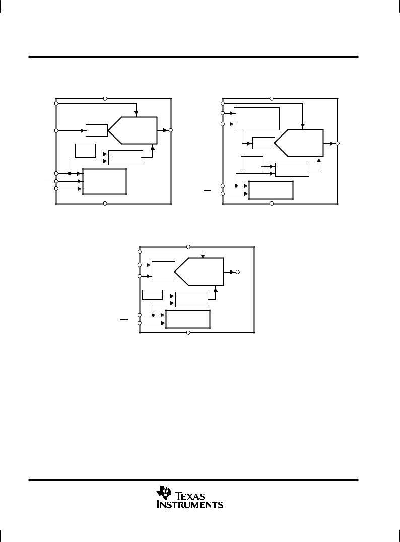
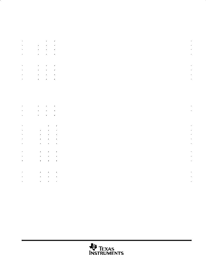
functional block diagram
TLV2541 |
TLV2542 |
VDD
REF |
|
|
|
|
|
S/H |
LOW POWER |
AIN |
|
12-BIT |
|
|
|
|
SAR ADC |
|
OSC |
Conversion |
|
|
|
||
|
|
|
Clock |
SCLK |
|
CONTROL |
|
CS |
|
|
|
|
LOGIC |
|
|
FS |
|
|
|
|
|
|
|
|
|
GND |
|
VDD
REF |
|
|
|
|
AIN0 |
Mux |
|
|
|
|
|
|
||
AIN1 |
|
|
|
|
SDO |
|
|
|
|
|
|
S/H |
LOW POWER |
SDO |
|
|
SAR ADC |
||
|
|
|
|
|
|
OSC |
Conversion |
|
|
|
|
|
||
|
|
|
Clock |
|
SCLK |
|
CONTROL |
|
|
CS/FS |
|
LOGIC |
|
|
|
|
GND |
|
|
TLV2545 |
|
|
|
|
VDD
REF |
|
|
AIN (+) |
LOW POWER |
|
S/H |
12-BIT |
SDO |
AIN (±) |
SAR ADC |
|
|
|
|
OSC |
Conversion |
|
|
Clock |
|
SCLK |
CONTROL |
|
CS/FS |
LOGIC |
|
|
GND |
|
2 |
POST OFFICE BOX 655303 •DALLAS, TEXAS 75265 |
|
|
|
|
|
|
|
|
|
|
|
|
|
|
|
|
|
|
|
TLV2541, TLV2542, TLV2545 |
|||||||
|
|
|
|
|
|
|
|
|
|
|
2.7 V TO 5.5 V, LOW POWER, 12-BIT, 200 KSPS, |
|||||||||||||||
|
|
|
|
|
|
|
|
|
SERIAL ANALOG-TO-DIGITAL CONVERTERS WITH AUTOPOWER DOWN |
|||||||||||||||||
|
|
|
|
|
|
|
|
|
|
|
|
|
|
|
|
|
|
|
SLAS245 ±MARCH 2000 |
|||||||
|
|
|
|
|
|
|
|
|
|
|
|
|
|
|
|
|
|
|
|
|
|
|
|
|
|
|
|
|
|
|
|
|
|
|
|
|
|
Terminal Functions |
|||||||||||||||
TLV2541 |
|
|
|
|
|
|
|
|
|
|
|
|
|
|
|
|
|
|
|
|
|
|
|
|||
|
|
|
|
|
|
|
|
|
|
|
|
|
|
|
|
|
|
|
|
|
|
|
|
|
|
|
|
TERMINAL |
|
I/O |
|
|
|
|
|
|
DESCRIPTION |
|
|||||||||||||||
|
|
|
|
|
|
|
|
|
|
|
|
|
|
|||||||||||||
|
NAME |
|
NO. |
|
||||||||||||||||||||||
|
|
|
|
|
|
|
|
|
|
|
|
|
|
|
|
|
|
|
|
|
|
|
||||
|
|
|
|
|
|
|
|
|
|
|
|
|
|
|
|
|
|
|
|
|
|
|
|
|
|
|
|
AIN |
|
4 |
|
I |
Analog input channel |
|
|||||||||||||||||||
|
|
|
|
|
|
|
|
|
|
|
|
|
|
|
|
|
|
|
|
|
|
|
|
|
|
|
|
|
|
|
1 |
|
I |
Chip select. A high-to-low transition on the |
|
|
input removes SDO from 3-state within a maximum setup time. |
|
|||||||||||||||
|
CS |
|
|
|
CS |
|
|
|||||||||||||||||||
|
|
|
|
|
|
|
|
CS can be used as the FS pin when a dedicated serial port is used. If TLV2541 is attached to a dedicated DSP serial |
|
|||||||||||||||||
|
|
|
|
|
|
|
|
port, this terminal can be grounded. |
|
|||||||||||||||||
|
|
|
|
|
|
|
|
|
|
|
|
|
|
|
|
|
|
|
|
|
|
|
|
|||
|
FS |
|
7 |
|
I |
DSP frame sync input. Indication of the start of a serial data frame. Tie this terminal to VDD if not used. |
|
|||||||||||||||||||
|
GND |
|
3 |
|
I |
Ground return for the internal circuitry. Unless otherwise noted, all voltage measurements are with respect to GND. |
|
|||||||||||||||||||
|
|
|
|
|
|
|
|
|
|
|
|
|
|
|
|
|
|
|
|
|
|
|
|
|||
|
SCLK |
|
5 |
|
I |
Output serial clock. This terminal receives the serial SCLK from the host processor. |
|
|||||||||||||||||||
|
|
|
|
|
|
|
|
|
|
|
|
|
|
|
|
|
|
|
|
|
|
|
|
|||
|
|
|
|
|
|
|
|
|
|
|
|
|
|
|
|
|
|
|
|
|
|
|||||
|
SDO |
|
8 |
|
O |
The 3-state serial output for the A/D conversion result. SDO is kept in the high-impedance state until |
CS |
|
falling edge. |
|
||||||||||||||||
|
|
|
|
|
|
|
|
The output format is MSB first. |
|
|||||||||||||||||
|
|
|
|
|
|
|
|
|
|
|
|
|
|
|
|
|
|
|
|
|
|
|
||||
|
|
|
|
|
|
|
|
When FS is not used (FS = 1 at the falling edge of |
CS): The MSB is presented to the SDO pin after CS falling edge |
|
||||||||||||||||
|
|
|
|
|
|
|
|
and output data is valid on the falling edge of SCLK. |
|
|||||||||||||||||
|
|
|
|
|
|
|
|
|
|
|
|
|
|
|
|
|
|
|
||||||||
|
|
|
|
|
|
|
|
When FS is used (FS = 0 at the falling edge of |
CS): The MSB is presented to the SDO pin after the falling edge of |
|
||||||||||||||||
|
|
|
|
|
|
|
|
FS or the falling edge of |
CS |
(whichever happens first). Output data is valid on the falling edge of SCLK. (This is |
|
|||||||||||||||
|
|
|
|
|
|
|
|
typically used with an active FS from a DSP). |
|
|||||||||||||||||
|
|
|
|
|
|
|
|
|
|
|
|
|
|
|||||||||||||
|
VDD |
|
6 |
|
I |
Positive supply voltage |
|
|||||||||||||||||||
|
VREF |
|
2 |
|
I |
External reference input |
|
|||||||||||||||||||
TLV2542/45 |
|
|
|
|
|
|
|
|
|
|
|
|
|
|
|
|
|
|
|
|
|
|||||
|
|
|
|
|
|
|
|
|
|
|
|
|
|
|
|
|
|
|
|
|
|
|
|
|
||
|
|
TERMINAL |
|
I/O |
|
|
|
|
|
|
DESCRIPTION |
|
||||||||||||||
|
|
|
|
|
|
|
|
|
|
|
|
|
|
|||||||||||||
|
|
NAME |
|
NO. |
|
|
|
|
|
|
|
|
||||||||||||||
|
|
|
|
|
|
|
|
|
|
|
|
|
|
|
|
|
|
|
|
|
|
|
|
|||
|
|
|
|
|
|
|
|
|
|
|
|
|
||||||||||||||
|
AIN0 /AIN(+) |
|
4 |
|
I |
|
Analog input channel 0. (positive input for TLV2545) |
|
||||||||||||||||||
|
|
|
|
|
|
|
|
|
|
|
|
|
||||||||||||||
|
AIN1/AIN (±) |
|
5 |
|
I |
|
Analog input channel 1 (inverted input for TLV2545) |
|
||||||||||||||||||
|
|
|
|
|
|
|
|
|
|
|
|
|
||||||||||||||
|
|
|
|
|
1 |
|
I |
|
Chip select/frame sync. A high-to-low transition on the |
|
|
|
|
|
|
|
|
|
||||||||
|
CS/FS |
|
|
|
CS/FS removes SDO from 3-state within a maximum delay |
|
||||||||||||||||||||
|
|
|
|
|
|
|
|
|
time. |
|
||||||||||||||||
|
|
|
|
|
|
|
|
|
|
|
||||||||||||||||
|
GND |
|
3 |
|
I |
|
Ground return for the internal circuitry. Unless otherwise noted, all voltage measurements are with respect to GND. |
|
||||||||||||||||||
|
|
|
|
|
|
|
|
|
|
|
||||||||||||||||
|
SCLK |
|
7 |
|
I |
|
Output serial clock. This terminal receives the serial SCLK from the host processor. |
|
||||||||||||||||||
|
|
|
|
|
|
|
|
|
||||||||||||||||||
|
SDO |
|
8 |
|
O |
|
The 3-state serial output for the A/D conversion result. SDO is kept in the high-impedance state when |
|
|
|
||||||||||||||||
|
|
|
|
CS/FS is |
|
|||||||||||||||||||||
|
|
|
|
|
|
|
|
|
high and presents output data after the CS/FS falling edge until the LSB is presented. The output format is MSB |
|
||||||||||||||||
|
|
|
|
|
|
|
|
|
first. SDO returns to the Hi-Z state after the 16th SCLK. Output data is valid on the falling SCLK edge. |
|
||||||||||||||||
|
VDD |
|
6 |
|
I |
|
Positive supply voltage |
|
||||||||||||||||||
|
VREF |
|
2 |
|
I |
|
External reference input |
|
||||||||||||||||||
detailed description
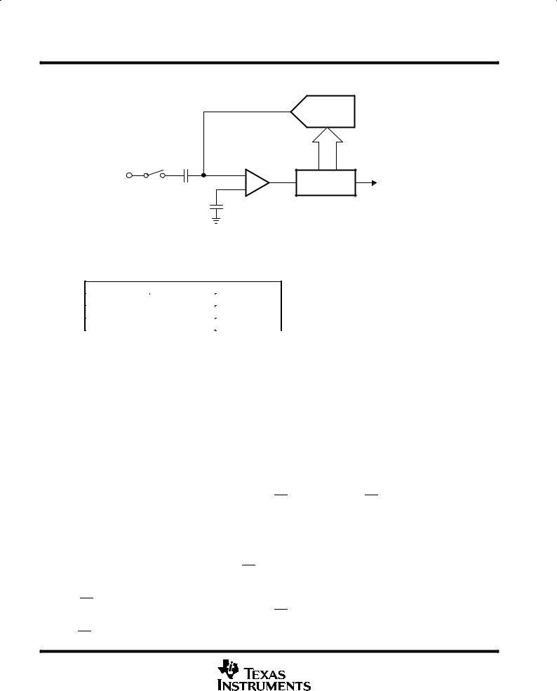
The TLV2541/2/5 are successive approximation (SAR) ADCs utilizing a charge redistribution DAC. Figure 1 shows a simplified version of the ADC.
The sampling capacitor acquires the signal on AIN during the sampling period. When the conversion process starts, the SAR control logic and charge redistribution DAC are used to add and subtract fixed amounts of charge from the sampling capacitor to bring the comparator into a balanced condition. When the comparator is balanced, the conversion is complete and the ADC output code is generated.
POST OFFICE BOX 655303 •DALLAS, TEXAS 75265 |
3 |
TLV2541, TLV2542, TLV2545
2.7 V TO 5.5 V, LOW POWER, 12-BIT, 200 KSPS,
SERIAL ANALOG-TO-DIGITAL CONVERTERS WITH AUTOPOWER DOWN
SLAS245 ±MARCH 2000
detailed description (continued)
Charge
Redistribution
DAC
AIN |
_ |
Control |
|
|
ADC Code |
||
|
+ |
Logic |
|
|
|
||
|
|
|
GND/AIN(±)
Figure 1. Simplified SAR Circuit
serial interface
OUTPUT DATA FORMAT
MSB |
LSB |
|
|
D15±D4 |
D3±D0 |
|
|
Conversion result (OD11±OD0) |
Don't care |
The output data format is binary (unipolar straight binary).
binary
Zero scale code = 000h, Vcode = GND
Full scale code = FFFh, Vcode = VREFP ± 1 LSB
pseudo-differential inputs
The TLV2545 operates in pseudo-differential mode. The inverted input is available on pin 5. It can have a maximum input ripple of ±0.2 V. This is normally used for ground noise rejection.
control and timing
start of the cycle
TLV2541
DWhen FS is not used ( FS = 1 at the falling edge of CS), the falling edge of CS is the start of the cycle. Output data changes on the rising edge of SCLK. This is typically used for a microcontroller with SPI interface, although it can also be used for a DSP. The microcontroller SPI interface should be programmed for CPOL=0 (serial clock referenced to ground) and CPHA=1 (data is valid on the falling edge of serial clock).
DWhen FS is used ( FS is an active signal from a DSP), the falling edge of FS is the start of the cycle. Output data changes on the rising edge of SCLK. This is typically used for a TMS320 DSP. If the TLV2541 is attached to a dedicated DSP serial port. CS terminal can be grounded.
TLV2542/5
The CS and FS inputs are accessed via the same pin (pin 1) on the TLV2542 and TLV2545. The cycle is started by the falling edge transition provided by either a CS (interfacing with SPI microcontroller) signal or FS (interfacing with TMS320 DSP) signal. Timing for the TLV2545 is much like the TLV2541, with the exception of the CS/FS line.
4 |
POST OFFICE BOX 655303 •DALLAS, TEXAS 75265 |
TLV2541, TLV2542, TLV2545 2.7 V TO 5.5 V, LOW POWER, 12-BIT, 200 KSPS, SERIAL ANALOG-TO-DIGITAL CONVERTERS WITH AUTOPOWER DOWN
SLAS245 ±MARCH 2000
detailed description (continued)
TLV2542 channel MUX reset cycle
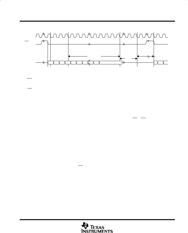
The TLV2542 uses CS/FS to reset the AIN multiplexer. A short active CS/FS cycle (4 to 7 SCLKs) resets the MUX to AIN0. If the CS/FS cycle is sufficient to complete the conversion (16 SCLKs plus maximum conversion time), the MUX toggles to the next channel (see Figure 4 for timing).
sampling
The converter sample time is 12 SCLKs in duration, beginning on the 5th SCLK received after the converter has received an active CS or FS signal (CS/FS for the TLV2542/5).
conversion
The TLV2541 completes conversion in the following manner. The conversion is started after the 16th SCLK edge. The conversion takes 3.5 s plus 0.1 s overhead. Enough time (for conversion) should be allowed before a rising CS/FS edge so that no conversion is terminated prematurely.
TLV2542 input channel selection is toggled on each rising CS /FS edge. The MUX channel can be reset to AIN0 via CS /FS as described in the earlier section and in Figure 5. The input is sampled for 12 SCLKs, converted, and the result is presented on SDO during the next cycle. Care should also be taken to allow enough time between samples to avoid prematurely terminating the conversion, which occurs on a rising CS /FS transition if the conversion is not complete.
POST OFFICE BOX 655303 •DALLAS, TEXAS 75265 |
5 |

TLV2541, TLV2542, TLV2545
2.7 V TO 5.5 V, LOW POWER, 12-BIT, 200 KSPS,
SERIAL ANALOG-TO-DIGITAL CONVERTERS WITH AUTOPOWER DOWN
SLAS245 ±MARCH 2000
timing diagrams/conversion cycles
DSP Interface
1 |
2 |
3 |
4 |
5 |
6 |
12 |
13 |
14 |
15 |
16 |
1 |
SCLK
CS
FS
t(sample) |
t(powerdown) |
tc
SDO |
OD11 |
OD10 OD9 OD8 OD7 OD6 |
OD0 |
Figure 2. TLV2541 DSP Mode/FS Active
P Interface
1 |
2 |
3 |
4 |
5 |
6 |
7 |
12 |
13 |
14 |
15 |
16 |
1 |
SCLK
CS
FS
|
|
|
|
|
|
|
t(sample) |
|
tc |
|
|
t(powerdown) |
|
|
|
|
|
|
|
|
|
|
|
|
|
SDO |
OD11 |
OD10 |
OD9 |
OD8 OD7 |
OD6 |
OD5 |
OD0 |
|
|
|
|
|
|
Figure 3. TLV2541 Microcontroller Mode/FS (SPI, CPOL = 0, CPHA = 1) |
|
||||||||||
1 |
2 |
3 |
4 |
5 |
1 |
4 |
12 |
16 |
1 |
4 |
12 |
16 |
SCLK |
|
|
|
|
|
|
|
|
|
|
|
|
|
|
<8 SCLKs, MUX |
|
|
|
|
>8 SCLKs, MUX Toggles to AIN1 |
|||||
CS/FS |
|
|
|
|
|
|
|
|
|
|||
|
Resets to AIN0 |
|
|
|
|
|
|
|
|
|||
|
|
|
|
|
|
|
|
|
t(powerdown) |
|
||
|
|
|
|
|
t(sample) |
|
tc |
|
|
t(sample) |
tc |
|
|
|
|
|
|
|
|
|
AIN0 Result |
|
|
||
|
|
|
|
|
|
|
|
|
|
|
|
|
SDO |
|
|
|
|
|
|
|
|
OD11 |
|
OD0 |
|
Figure 4. TLV2542 Timing
6 |
POST OFFICE BOX 655303 •DALLAS, TEXAS 75265 |
TLV2541, TLV2542, TLV2545 2.7 V TO 5.5 V, LOW POWER, 12-BIT, 200 KSPS, SERIAL ANALOG-TO-DIGITAL CONVERTERS WITH AUTOPOWER DOWN
SLAS245 ±MARCH 2000
timing diagrams/conversion cycles (continued)
1 |
2 |
3 |
4 |
5 |
6 |
7 |
12 |
13 |
14 |
15 |
16 |
1 |
SCLK
CS/FS
t(sample) |
t(powerdown) |
tc
SDO
OD11 |
OD10 |
OD9 |
OD8 |
OD7 |
OD6 |
OD5 |
OD0 |
OD11 OD10 |
OD9 |
Figure 5. TLV2545 Timing
use CS as FS input
When interfacing the TLV2541 with the TMS320 DSP, the FSR signal from the DSP may be connected to the CS input if this is the only device on the serial port. This will save one output terminal from the DSP. (Output data changes on the falling edge of SCLK. Default for TLV2542 and TLV2545).
SCLK and conversion speed
The minimum onboard oscillator frequency for the TLV2541/2/5 is 4 MHz, and it takes 14 conversion clocks to complete the conversion. This leads to a 3.5 µs conversion time plus 0.1 µs overhead. These devices can operate with an SCLK up to 20 MHz for the supply voltage range specified. The total conversion time is
14×(1/fosc). For a 20 MHz SCLK, the minimum total cycle time is given by: 14×(1/4M) +16×(1/20M)+ 0.1 µs} = 4.4 µs for the TLV254x devices. This is the minimum cycle time for an active CS or CS/FS signal. If violated,
the conversion will terminate, invalidating the next data output cycle.
reference voltage
An external reference is applied via VREF. The voltage level applied to this pin establishes the upper limit of the analog inputs to produce a full-scale reading. The value of VREF and the analog input should not exceed the positive supply or be less than GND, consistent with the specified absolute maximum ratings. The digital output is at full scale when the input signal is equal to or higher than VREF and at zero when the input signal is equal to or lower than GND.
powerdown and powerup initialization
Autopower down is built in to the devices in order to reduce power consumption. The wake-up time is fast enough to provide power down between each cycle. The power-down state is initiated at the end of conversion and wakes up upon a falling edge on CS or FS.
POST OFFICE BOX 655303 •DALLAS, TEXAS 75265 |
7 |
TLV2541, TLV2542, TLV2545
2.7 V TO 5.5 V, LOW POWER, 12-BIT, 200 KSPS,
SERIAL ANALOG-TO-DIGITAL CONVERTERS WITH AUTOPOWER DOWN
SLAS245 ±MARCH 2000
absolute maximum ratings over operating free-air temperature (unless otherwise noted)²
Supply voltage range, GND to VDD . . . . . . . . . . . . . . . . . . . . . . . . . . . . . . . . . . . . . . . . . . . |
. . . . . . ±0.3 V to 6.5 |
V |
Analog input voltage range . . . . . . . . . . . . . . . . . . . . . . . . . . . . . . . . . . . . . . . . . . . . . . . . . . . |
±0.3 V to VDD + 0.3 |
V |
Reference input voltage . . . . . . . . . . . . . . . . . . . . . . . . . . . . . . . . . . . . . . . . . . . . . . . . . . . . . . |
. . . . . . . VDD + 0.3 |
V |
Digital input voltage range . . . . . . . . . . . . . . . . . . . . . . . . . . . . . . . . . . . . . . . . . . . . . . . . . . . |
±0.3 V to VDD+ 0.3 |
V |
Operating virtual junction temperature range, TJ . . . . . . . . . . . . . . . . . . . . . . . . . . . . . . . . . |
. . . . ±40°C to 150°C |
|
Operating free-air temperature range, TA: C . . . . . . . . . . . . . . . . . . . . . . . . . . . . . . . . . . . . |
. . . . . . . 0°C to 70°C |
|
I . . . . . . . . . . . . . . . . . . . . . . . . . . . . . . . . . . . . . |
. . . . . ±40°C to 85°C |
|
Storage temperature range, Tstg . . . . . . . . . . . . . . . . . . . . . . . . . . . . . . . . . . . . . . . . . . . . . . . |
. . . . ±65°C to 150°C |
|
Lead temperature 1,6 mm (1/16 inch) from case for 10 seconds . . . . . . . . . . . . . . . . . . . |
. . . . . . . . . . . . 260°C |
|
²Stresses beyond those listed under ªabsolute maximum ratingsº may cause permanent damage to the device. These are stress ratings only, and functional operation of the device at these or any other conditions beyond those indicated under ªrecommended operating conditionsº is not implied. Exposure to absolute-maximum-rated conditions for extended periods may affect device reliability.
recommended operating conditions
|
|
|
|
|
|
|
|
|
|
|
|
|
|
MIN |
NOM |
MAX |
UNIT |
|
|
|
|
|
|
|
|
|
|
|
|
|
|
|
|
|
|
Supply voltage, VDD |
|
2.7 |
3.3 |
5.5 |
V |
||||||||||||
Positive external reference voltage input, VREFP (see Note 1) |
|
2 |
|
VDD |
V |
||||||||||||
Analog input voltage (see Note 1) |
|
0 |
|
VDD |
V |
||||||||||||
High level control input voltage, VIH |
|
2.1 |
|
|
V |
||||||||||||
Low-level control input voltage, VIL |
|
|
|
0.6 |
V |
||||||||||||
Setup time, |
|
|
|
|
falling edge (2541) or |
|
|
VDD = REF = 5 V |
40 |
|
|
|
|||||
CS |
CS/FS falling edge (2542/45) |
|
|
ns |
|||||||||||||
before first SCLK falling edge, tsu(CSL-SCLKL) |
V = REF = 2.7 V |
70 |
|
|
|||||||||||||
|
|
|
|||||||||||||||
|
|
|
|
|
|
|
|
|
|
|
|
|
DD |
|
|
|
|
Hold time, |
CS |
rising edge after SCLK falling edge, th(SCLKL-CSH) |
|
5 |
|
|
ns |
||||||||||
Delay time, delay from |
CS |
falling edge to FS rising edge (td(CSL-FSH) |
0.5 |
|
7 |
SCLKs |
|||||||||||
Setup time, FS rising edge before SCLK falling edge, tsu(FSH-SCLKL) |
0.35 |
|
|
SCLKs |
|||||||||||||
Hold time, FS hold high after SCLK falling edge, th(SCLKL-FSL) |
|
|
|
0.65 |
SCLKs |
||||||||||||
Pulse width |
CS |
high time, twH(CS) |
|
100 |
|
|
ns |
||||||||||
Pulse width FS high time, twH(FS) |
|
0.75 |
|
|
SCLKs |
||||||||||||
SCLK cycle time, VDD = 3.6±2.7 V, tc(SCLK) |
|
67 |
|
10000 |
ns |
||||||||||||
SCLK cycle time, VDD = 5.5±4.5 V, tc(SCLK) |
|
50 |
|
10000 |
ns |
||||||||||||
Pulse width low time, twL(SCLK) |
|
0.4 |
|
0.6 |
SCLK |
||||||||||||
Pulse width high time, twH(SCLK) |
|
0.4 |
|
0.6 |
SCLK |
||||||||||||
Hold time, hold from end of conversion to CS high, th(EOC-CSH) (EOC is internal, indicates end of |
0.1 |
|
|
s |
|||||||||||||
conversion time, tc) |
|
|
|
|
|
||||||||||||
Active |
CS/FS cycle time to reset internal MUX to AIN0, reset cycle |
TLV2542 only |
4 |
|
7 |
SCLKs |
|||||||||||
|
|
|
|
|
|
|
|
|
|
|
|
|
|
|
|
|
|
Operating free-air temperature, TA |
TLV2541/2/5C |
0 |
|
70 |
°C |
||||||||||||
|
|
|
|
||||||||||||||
TLV2541/2/5I |
±40 |
|
85 |
||||||||||||||
|
|
|
|
|
|
|
|
|
|
|
|
|
|
|
|||
|
|
|
|
|
|
|
|
|
|
|
|
|
|
|
|
|
|
NOTES: 1. Analog input voltages greater than that applied to VREF convert as all ones (111111111111), while input voltages less than that applied to GND convert as all zeros(000000000000).
2.This is the time required for the clock input signal to fall from VIH max or to rise from VILmax to VIHmin. In the vicinity of normal room temperature, the devices function with input clock transition time as slow as 1 s for remote data-acquisition applications where the sensor and A/D converter are placed several feet away from the controlling microprocessor.
8 |
POST OFFICE BOX 655303 •DALLAS, TEXAS 75265 |
 Loading...