


Texas Instruments TL031ID, TL031CPWLE, TL031CPS, TL031CP, TL031CDR Datasheet
...
|
TL03x, TL03xA, TL03xY |
|
|
ENHANCED-JFET LOW-POWER LOW-OFFSET |
|
|
OPERATIONAL AMPLIFIERS |
|
|
SLOS180B ± FEBRUARY 1997 ± REVISED FEBRUARY 1999 |
|
|
|
|
D Direct Upgrades for the TL06x Low-Power |
D Higher Slew Rate and Bandwidth Without |
|
BiFETs |
Increased Power Consumption |
|
D Low Power Consumption . . . |
D Available in TSSOP for Small Form-Factor |
|
6.5 mW/Channel Typ |
Designs |
|
D On-Chip Offset-Voltage Trimming for |
|
|
Improved DC Performance |
|
|
(1.5 mV, TL031A) |
|
|
description
The TL03x series of JFET-input operational amplifiers offer improved dc and ac characteristics over the TL06x family of low-power BiFET operational amplifiers. On-chip zener trimming of offset voltage yields precision grades as low as 1.5 mV (TL031A) for greater accuracy in dc-coupled applications. Texas Instruments improved BiFET process and optimized designs also yield improved bandwidths and slew rates without increased power consumption. The TL03x devices are pin-compatible with the TL06x and can be used to upgrade existing circuits or for optimal performance in new designs.
BiFET operational amplifiers offer the inherently higher input impedance of the JFET-input transistors without sacrificing the output drive associated with bipolar amplifiers. This higher input impedance makes the TL3x amplifiers better suited for interfacing with high-impedance sensors or very low-level ac signals. These devices also feature inherently better ac response than bipolar or CMOS devices having comparable power consumption.
The TL03x family has been optimized for micropower operation, while improving on the performance of the TL06x series. Designers requiring significantly faster ac response should consider the Excalibur TLE206x family of low-power BiFET operational amplifiers.
Because BiFET operational amplifiers are designed for use with dual power supplies, care must be taken to observe common-mode input-voltage limits and output swing when operating from a single supply. DC biasing of the input signal is required and loads should be terminated to a virtual-ground node at midsupply. Texas Instruments TLE2426 integrated virtual-ground generator is useful when operating BiFET amplifiers from single supplies.
The TL03x devices are fully specified at ±15 V and ±5 V. For operation in low-voltage and/or single-supply systems, Texas Instruments LinCMOS families of operational amplifiers (TLC-prefix) are recommended. When moving from BiFET to CMOS amplifiers, particular attention should be paid to slew rate, bandwidth requirements, and output loading.
The C-suffix devices are characterized for operation from 0°C to 70°C. The I-suffix devices are characterized for operation from ±40°C to 85°C. The M-suffix devices are characterized for operation over the full military temperature range of ±55°C to 125°C.
Please be aware that an important notice concerning availability, standard warranty, and use in critical applications of Texas Instruments semiconductor products and disclaimers thereto appears at the end of this data sheet.
PRODUCTION DATA information is current as of publication date. Products conform to specifications per the terms of Texas Instruments standard warranty. Production processing does not necessarily include testing of all parameters.
Copyright 1999, Texas Instruments Incorporated
POST OFFICE BOX 655303 •DALLAS, TEXAS 75265 |
1 |
TL03x, TL03xA, TL03xY
ENHANCED-JFET LOW-POWER LOW-OFFSET OPERATIONAL AMPLIFIERS
SLOS180B ± FEBRUARY 1997 ± REVISED FEBRUARY 1999
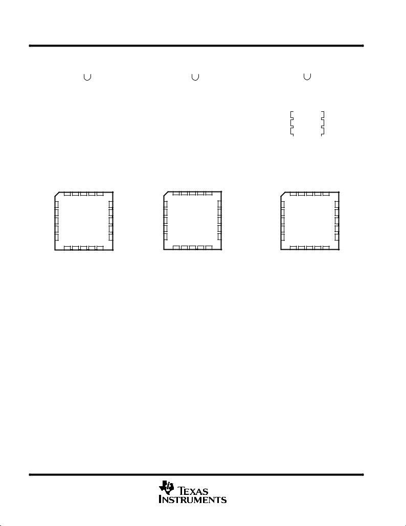
TL031x, TL031Ax D, JG, OR P PACKAGE
(TOP VIEW)
OFFSET N1 |
|
|
1 |
8 |
|
NC |
|
|
|||||
IN± |
|
|
2 |
7 |
|
VCC+ |
IN+ |
|
|
3 |
6 |
|
OUT |
VCC± |
|
|
4 |
5 |
|
OFFSET N2 |
|
|
|
|
|
|
|
TL031M, TL031AM FK PACKAGE (TOP VIEW)
|
NC |
OFFSET N1 |
NC |
NC |
NC |
|
NC |
3 |
2 |
1 |
20 19 |
NC |
|
4 |
|
|
|
18 |
||
IN± |
5 |
|
|
|
17 |
VCC+ |
NC |
6 |
|
|
|
16 |
NC |
IN+ |
7 |
|
|
|
15 |
OUT |
NC |
8 |
|
|
|
14 |
NC |
|
9 |
10 11 12 13 |
|
|||
NC |
CC± NC |
N2 |
NC |
|
V |
OFFSET |
|
NC ± No internal connection
TL032x, TL032Ax D, JG, OR P PACKAGE
(TOP VIEW)
1OUT |
|
1 |
8 |
|
VCC+ |
|
|
||||
1IN± |
|
|
|
|
|
|
2 |
7 |
|
2OUT |
|
1IN+ |
|
3 |
6 |
|
2IN± |
|
|
||||
VCC ± |
|
4 |
5 |
|
2IN+ |
|
|
||||
|
|
|
|
|
|
|
|
|
|
|
|
|
TL032M, TL032AM |
|
|||
|
FK PACKAGE |
|
|||
|
NC |
(TOP VIEW) |
|
||
|
1OUT |
NC |
V NC |
|
|
|
|
|
|
CC+ |
|
NC |
3 |
2 |
1 |
20 19 |
NC |
4 |
|
|
18 |
||
1IN± |
5 |
|
|
17 |
2OUT |
NC |
6 |
|
|
16 |
NC |
1IN+ |
7 |
|
|
15 |
2IN± |
NC |
8 |
|
|
14 |
NC |
|
9 |
10 11 12 13 |
|
||
|
NC |
CC± |
NC |
2IN+ NC |
|
|
V |
|
|||
TL034x, TL034Ax
D, J, N, OR PW PACKAGE
(TOP VIEW)
1OUT |
|
1 |
14 |
|
4OUT |
|
|
||||
1IN± |
|
2 |
13 |
|
4IN± |
|
|
||||
1IN+ |
|
3 |
12 |
|
4IN+ |
|
|
||||
VCC+ |
|
4 |
11 |
|
VCC± |
|
|
||||
|
|
||||
2IN+ |
5 |
10 |
|
3IN+ |
|
2IN± |
6 |
9 |
|
3IN± |
|
2OUT |
7 |
8 |
|
3OUT |
|
|
|
|
|
|
|
TL034M, TL034AM FK PACKAGE (TOP VIEW)
|
1IN± |
1OUT |
NC |
4OUT |
4IN± |
|
1IN+ |
3 |
2 |
1 |
20 19 |
4IN+ |
|
4 |
|
|
|
18 |
||
NC |
5 |
|
|
|
17 |
NC |
VCC+ |
6 |
|
|
|
16 |
VCC± |
NC |
7 |
|
|
|
15 |
NC |
2IN+ |
8 |
|
|
|
14 |
3IN+ |
|
9 |
10 11 12 13 |
|
|||
|
2IN± |
2OUT |
NC |
3OUT |
3IN± |
|
2 |
POST OFFICE BOX 655303 •DALLAS, TEXAS 75265 |
TL03x, TL03xA, TL03xY
ENHANCED-JFET LOW-POWER LOW-OFFSET
OPERATIONAL AMPLIFIERS
SLOS180B ± FEBRUARY 1997 ± REVISED FEBRUARY 1999
AVAILABLE OPTIONS
|
|
|
|
PACKAGED DEVICES |
|
|
CHIP |
|||
|
VIOMAX |
|
|
|
|
|
|
|
||
T |
SMALL |
CHIP |
CERAMIC |
CERAMIC |
PLASTIC |
PLASTIC |
² |
|||
FORM³ |
||||||||||
A |
AT 25°C |
OUTLINE² |
CARRIER |
DIP |
DIP |
DIP |
DIP |
TSSOP |
(Y) |
|
|
(PW) |
|||||||||
|
|
(D) |
(FK) |
(J) |
(JG) |
(N) |
(P) |
|||
|
|
|
|
|||||||
|
|
|
|
|
|
|
|
|
|
|
|
0.8 mV |
TL031ACD |
Ð |
Ð |
Ð |
Ð |
TL031ACP |
Ð |
|
|
|
TL032ACD |
TL032ACP |
|
|||||||
|
|
|
|
|
|
|
|
|||
|
|
|
|
|
|
|
|
|
TL031Y |
|
0°C to 70°C |
|
TL031CD |
|
|
|
|
TL031CP |
|
||
|
|
|
|
|
|
TL032Y |
||||
1.5 mV |
TL032CD |
Ð |
Ð |
Ð |
TL034ACN |
Ð |
||||
|
TL032CP |
TL034Y |
||||||||
|
|
TL034ACD |
|
|
|
|
|
|||
|
|
|
|
|
|
|
|
|
||
|
|
|
|
|
|
|
|
|
|
|
|
4 mV |
TL034CD |
Ð |
Ð |
Ð |
TL034CN |
|
TL034CPW |
|
|
|
|
|
|
|
|
|
|
|
|
|
|
0.8 mV |
TL031AID |
Ð |
Ð |
Ð |
Ð |
TL031AIP |
Ð |
Ð |
|
|
TL032AID |
TL032AIP |
||||||||
|
|
|
|
|
|
|
|
|||
|
|
|
|
|
|
|
|
|
|
|
±40°C to 85°C |
|
TL031ID |
|
|
|
|
TL031IP |
|
|
|
1.5 mV |
TL032ID |
Ð |
Ð |
Ð |
TL034AIN |
Ð |
Ð |
|||
|
TL032IP |
|||||||||
|
|
TL034AID |
|
|
|
|
|
|
||
|
|
|
|
|
|
|
|
|
||
|
|
|
|
|
|
|
|
|
|
|
|
4 mV |
TL034ID |
Ð |
Ð |
Ð |
TL034IN |
Ð |
Ð |
Ð |
|
|
|
|
|
|
|
|
|
|
|
|
|
0.8 mV |
TL031AMD |
TL031AMFK |
Ð |
TL031AMJG |
Ð |
TL031AMP |
Ð |
Ð |
|
|
TL032AMD |
TL032AMFK |
TL032AMJG |
TL032AMP |
||||||
|
|
|
|
|
|
|||||
|
|
|
|
|
|
|
|
|
|
|
±55°C to 125°C |
|
TL031MD |
TL031MFK |
|
TL031MJG |
|
TL031MP |
|
|
|
1.5 mV |
TL032MD |
TL032MFK |
TL034AMJ |
TL034AMN |
Ð |
Ð |
||||
|
TL032MJG |
TL032MP |
||||||||
|
|
TL034AMD |
TL034AMFK |
|
|
|
|
|||
|
|
|
|
|
|
|
|
|||
|
|
|
|
|
|
|
|
|
|
|
|
4 mV |
TL034MD |
TL034MFK |
TL034MJ |
Ð |
TL034MN |
Ð |
Ð |
Ð |
|
|
|
|
|
|
|
|
|
|
|
|
² The D and PW packages are available taped and reeled and are indicated by adding an R suffix to device type (e.g., TL034CDR or TL034CPWR). ³ Chip forms are tested at 25°C.
POST OFFICE BOX 655303 •DALLAS, TEXAS 75265 |
3 |
TL03x, TL03xA, TL03xY
ENHANCED-JFET LOW-POWER LOW-OFFSET
OPERATIONAL AMPLIFIERS
SLOS180B ± FEBRUARY 1997 ± REVISED FEBRUARY 1999
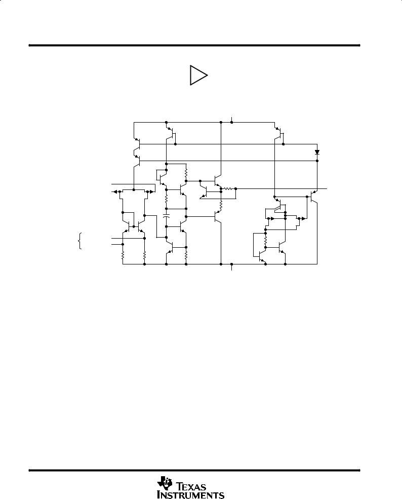
symbol (each amplifier)
IN± |
|
|
± |
|
OUT |
|
|
|
|||
IN+ |
|
|
+ |
|
|
|
|
|
|
||
|
|
|
equivalent schematic (each amplifier)
|
|
|
|
|
VCC+ |
|
|
|
|
Q5 |
|
|
Q14 |
|
Q2 |
|
|
|
|
|
|
|
|
|
|
|
D1 |
|
Q3 |
|
|
|
|
|
|
|
|
R4 |
|
|
|
IN+ |
|
|
Q6 |
|
Q11 |
|
|
|
Q8 |
|
|
OUT |
|
IN± |
JF1 |
JF2 |
Q10 |
R7 |
||
|
R3 |
|
Q17 |
|||
|
|
|
|
|
||
|
|
|
R6 |
|
Q15 |
|
|
|
|
|
|
||
|
|
|
C1 |
|
Q12 |
|
|
Q1 |
Q4 |
Q9 |
|
JF3 |
JF4 |
|
|
|
|
|||
(see Note A) |
OFFSET N1 |
|
|
R8 |
OFFSET N2 |
|
|
||
|
|
Q7 |
Q16 |
|
|
|
|
||
|
R1 |
R2 |
R5 |
Q13 |
VCC±
NOTE A: OFFSET N1 and OFFSET N2 are available only on the TL031.
4 |
POST OFFICE BOX 655303 •DALLAS, TEXAS 75265 |
TL03x, TL03xA, TL03xY
ENHANCED-JFET LOW-POWER LOW-OFFSET
OPERATIONAL AMPLIFIERS
SLOS180B ± FEBRUARY 1997 ± REVISED FEBRUARY 1999
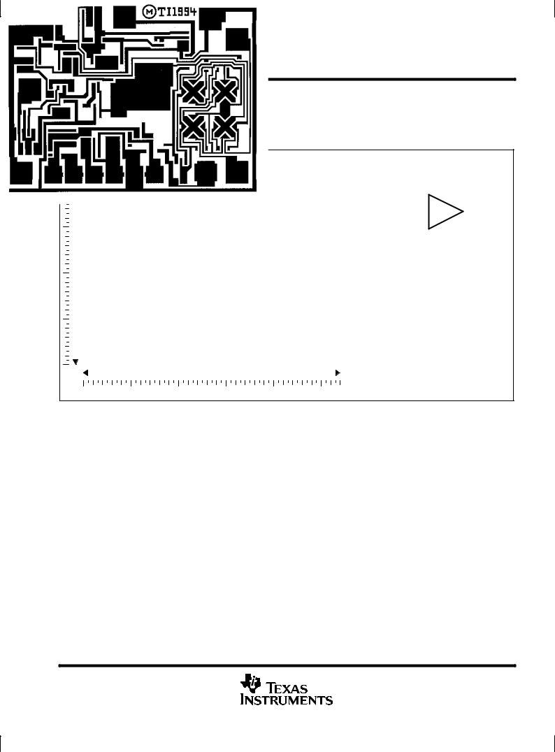
TL031Y chip information
This chip, when properly assembled, has characteristics similar to the TL031C. Thermal compression or ultrasonic bonding can be used on the doped-aluminum bonding pads. These chips can be mounted with conductive epoxy or a gold-silicon preform.
Bonding-Pad Assignments
|
|
|
|
(5) |
(4) |
|
|
|
|
|
|
(6) |
|
|
(3) |
|
|
|
|
|
|
|
|
|
|
|
|
(7) |
|
|
|
42 |
|
|
|
|
|||
|
|
|
|
(8) |
|
(1) |
(2) |
|
|
|
|
|
|||
|
|
|
|
|
|
|
|
|
|
|
|
|
|
|
|
|
|
|
|
VCC+ |
|
|
|||
|
|
(3) |
|
|
|
|
(7) |
|
|
IN+ |
+ |
|
|
|
|
|
|||
|
|
|
|
(6) |
|||||
|
|
|
|
|
|
|
|
||
IN± |
(2) |
± |
|
|
|
|
OUT |
||
|
|
|
|
||||||
|
|
|
|
|
|||||
|
|
|
(4) |
|
|
||||
(1) |
|
|
|||||||
|
|
|
|||||||
|
|
|
|
|
|
|
|
||
OFFSET N1 |
|
|
|
VCC± |
|
|
|||
|
|
|
|
|
|
||||
|
(5) |
|
|
|
|
||||
OFFSET N2 |
|
|
|
|
|
|
|
||
|
|
|
|
|
|
|
|
||
|
|
|
|
|
|
|
|
||
Chip Thickness: 15 MIls Typical Bonding Pads: 4 × 4 Mils Minimum TJ(max) = 150°C
Tolerances Are ±10%.
All Dimensions Are in Mils. Pin (4) is Internally Connected to Backside of the Chip.
POST OFFICE BOX 655303 •DALLAS, TEXAS 75265 |
5 |
TL03x, TL03xA, TL03xY
ENHANCED-JFET LOW-POWER LOW-OFFSET
OPERATIONAL AMPLIFIERS
SLOS180B ± FEBRUARY 1997 ± REVISED FEBRUARY 1999
TL032Y chip information
This chip, when properly assembled, has characteristics similar to the TL032C. Thermal compression or ultrasonic bonding can be used on the doped-aluminum bonding pads. These chips can be mounted with conductive epoxy or a gold-silicon preform.
Bonding-Pad Assignments
|
|
|
|
(7) |
(6) |
(5) |
||
|
|
(8) |
|
|
|
|||
|
|
|
|
|
|
|
||
67 |
|
|
|
|
(4) |
|||
|
|
(1) |
(2) |
(3) |
||||
|
|
|||||||
|
|
|
|
|
|
|
|
|
|
|
|
|
|
|
|
|
|
|
|
|
|
|
|
51 |
|
|
|
|
|
VCC+ |
|
|
|
||
|
(3) |
|
|
|
(8) |
|
|
|
1IN+ |
+ |
|
|
|
|
|
||
|
|
|
(1) |
|
1OUT |
|||
|
|
|
|
|
|
|
||
1IN± |
(2) |
± |
|
|
|
|
||
|
|
|
||||||
|
|
|
|
|
||||
|
|
|
(5) |
|
|
|||
|
|
|
||||||
|
|
+ |
|
2IN+ |
||||
2OUT |
(7) |
|
|
|||||
|
|
|||||||
|
|
|
|
|
|
|||
|
|
|
|
± |
(6) |
|
2IN± |
|
|
|
|
|
|
||||
|
|
|
|
|
|
|||
|
|
|
|
|
|
|||
|
|
|
|
|||||
|
|
|
|
(4) |
|
|
|
|
|
|
|
VCC± |
|
|
|
||
Chip Thickness: 15 Mils Typical Bonding Pads: 4 × 4 Mils Minimum TJ(max) = 150°C
Tolerances Are ±10%.
All Dimensions Are in Mils.
Pin (4) is Internally Connected to Backside of Chip.
6 |
POST OFFICE BOX 655303 •DALLAS, TEXAS 75265 |

TL03x, TL03xA, TL03xY
ENHANCED-JFET LOW-POWER LOW-OFFSET
OPERATIONAL AMPLIFIERS
SLOS180B ± FEBRUARY 1997 ± REVISED FEBRUARY 1999
TL034Y chip information
This chip, when properly assembled, has characteristics similar to the TL034C. Thermal compression or ultrasonic bonding can be used on the doped-aluminum bonding pads. These chips can be mounted with conductive epoxy or a gold-silicon preform.
Bonding-Pad Assignments
|
|
|
|
(13) |
|
|
|
|
(12) |
(11) |
|
|
(10) |
|
|
|
|
|
|
|
|
(9) |
|
|
|
|
|||||||||||||||||||||||||||||||||||||||||||||||||||||||||||||||||||||||
|
|
|
|
(14) |
|
|
|
|
|
|
|
|
|
|
|
|
|
|
|
|
|
|
|
|
|
|
|
|
|
|
|
|
|
|
|
|
|
|
|
|
|
|
|
|
|
|
|
|
|
|
|
|
|
|
|
|
|
|
|
(8) |
|
|
|
|
|||||||||||||||||||||||||||||||||
|
|
|
|
|
|
|
|
|
|
|
|
|
|
|
|
|
|
|
|
|
|
|
|
|
|
|
|
|
|
|
|
|
|
|
|
|
|
|
|
|
|
|
|
|
|
|
|
|
|
|
|
|
|
|
|
|
|
|
|
|
|
|
|
|
|
|
|
|
|
|
|
|
|
|
|
|
|
|
|
|
|
|
|
|
|
|
|
|
|
|
|
|
|
|
|
||
66 |
|
|
|
|
|
|
|
|
|
|
|
|
|
|
|
|
|
|
|
|
|
|
|
|
|
|
|
|
|
|
|
|
|
|
|
|
|
|
|
|
|
|
|
|
|
|
|
|
|
|
|
|
|
|
|
|
|
|
|
|
|
|
|
|
|
|
|
|
|
|
|
|
|
|
|
|
|
|
|
|
|
|
|
|
|
|
|
|
|
|
|
|
|
|
|||
|
|
|
|
(1) |
|
|
|
|
|
|
|
|
|
|
|
|
|
|
|
|
|
|
|
|
|
|
|
|
|
|
|
|
|
|
|
|
|
|
|
|
|
|
|
|
|
|
|
|
|
|
|
|
|
|
|
|
|
|
|
(7) |
|
|
|
|
|||||||||||||||||||||||||||||||||
|
|
|
|
|
|
|
|
|
|
|
|
|
|
|
|
|
|
|
|
|
|
|
|
|
|
|
|
|
|
|
|
|
|
|
|
|
|
|
|
|
|
|
|
|
|
|
|
|
|
|
|
|
|
|
|
|
|
|
|
|
|
|
|||||||||||||||||||||||||||||||||||
|
|
|
|
(2) |
|
|
|
|
|
|
(3) |
|
(4) |
|
|
(5) |
|
|
|
|
|
|
|
|
|
(6) |
|
|
|
|
|||||||||||||||||||||||||||||||||||||||||||||||||||||||||||||||||||
|
|
|
|
|
|
|
|
|
|
|
|
|
|
|
|
|
|
|
|
|
|
|
|
|
|
|
|
|
|
|
|
|
|
|
|
|
|
|
|
|
|
|
|
|
|
|
|
|
|
|
|
|
|
|
|
|
|
|
|
|
|
|
|
|
|
|
|
|
|
|
|
|
|
|
|
|
|
|
|
|
|
|
|
|
|
|
|
|
|
|
|
|
|
|
|
|
|
|
|
|
|
|
|
|
|
|
|
|
|
|
|
|
|
|
|
|
|
|
|
|
|
|
|
|
|
|
|
|
|
|
|
|
|
|
|
|
|
|
|
|
|
|
|
|
|
|
93 |
|
|
|
|
|
|
|
|
|
|
|
|
|
|
|
|
|
|
|
|
|
|
|
|
|
|
|
|
|
|
|
|
|
|
|
|
|
|
|
|
|
|
|
|
|
|||
|
|
|
|
|
|
|
|
|
|
|
|
|
|
|
|
|
|
|
|
|
|
|
|
|
|
|
|
|
|
|
|
|
|
|
|
|
|
|
|
|
|
|
|
|
|
|
|
|
|
|
|
|
|
|
|
|
|
|
|
|
|
|
|
|
|
|
|
|
|
|
|
|
|
|
|
|
|
|
|
|
|
|
|
|
|
|
|
|
|
|
|
||||||
|
|
|
|
|
|
|
|
|
|
|
|
|
|
|
|
|
|
|
|
|
|
|
|
|
|
|
|
|
|
|
|
|
|
|
|
|
|
|
|
|
|
|
|
|
|
|
|
|
|
|
|
|
|
|
|
|
|
|
|
|
|
|
|
|
|
|
|
|
|
|
|
|
|
|
|
|
|
|
|
|
|
|
|
|
|
|
|
|
|
|
|
|
|
|
|
|
|
|
|
|
VCC+ |
|
|
|
|
||
|
(3) |
|
|
|
(4) |
|
|
|
|
1IN+ |
+ |
|
|
|
|
|
|
||
|
|
|
(1) |
|
|
1OUT |
|||
(2) |
|
|
|||||||
1IN± |
± |
|
|
|
|
||||
|
|
|
|
|
|||||
|
|
|
|
||||||
|
|
|
|
|
|
||||
|
|
|
(5) |
|
|
|
|||
|
|
|
|
||||||
|
|
+ |
|
|
2IN+ |
||||
2OUT |
(7) |
|
|
|
|||||
|
|
|
|||||||
|
|
|
|
|
|
|
|||
|
|
|
|
|
(6) |
|
|
|
|
|
± |
|
|
2IN± |
|||||
|
|
|
|
||||||
3IN+ |
(10) |
|
|
|
|||||
|
|
|
|||||||
+ |
|
|
|
|
|
|
|||
|
|
|
(8) |
|
|
3OUT |
|||
|
|
|
|
|
|||||
|
|
|
|
|
|
|
|
||
3IN± |
(9) |
± |
|
|
|
|
|
||
|
|
|
|
|
|||||
|
|
|
|
|
|
||||
|
|
|
(12) |
|
|
||||
|
|
|
|
|
|||||
|
|
+ |
|
4IN+ |
|||||
4OUT |
(14) |
|
|
|
|||||
|
|
|
|||||||
|
|
|
|
|
|
|
|
||
|
|
|
± |
(13) |
|
4IN± |
|||
|
|
|
|
||||||
|
|
|
|
|
|||||
|
|
|
(11) |
|
|
|
|
||
|
|
|
VCC± |
|
|
|
|
||
Chip Thickness: 15 Mils Typical Bonding Pads: 4 × 4 Mils Minimum TJ(max) = 150°C
Tolerances Are ±10%.
All Dimensions Are in Mils.
Pin (11) is Internally Connected to Backside of the Chip.
POST OFFICE BOX 655303 •DALLAS, TEXAS 75265 |
7 |
TL03x, TL03xA, TL03xY
ENHANCED-JFET LOW-POWER LOW-OFFSET
OPERATIONAL AMPLIFIERS
SLOS180B ± FEBRUARY 1997 ± REVISED FEBRUARY 1999
absolute maximum ratings over operating free-air temperature range (unless otherwise noted)²
Supply voltage, VCC+ (see Note 1) . . . . . . . . . . . . . . . . . . . . . . . . . . . . . . . . . . . . . . |
. . . . . . . . . . . . |
. . . . . . . . 18 |
V |
Supply voltage, VCC± (see Note 1) . . . . . . . . . . . . . . . . . . . . . . . . . . . . . . . . . . . . . . |
. . . . . . . . . . . . |
. . . . . . . ±18 V |
|
Differential input voltage, VID (see Note 2) . . . . . . . . . . . . . . . . . . . . . . . . . . . . . . . |
. . . . . . . . . . . . |
. . . . . . . ±30 |
V |
Input voltage, VI (any input) (see Notes 1 and 3) . . . . . . . . . . . . . . . . . . . . . . . . . . |
. . . . . . . . . . . . |
. . . . . . . ±15 |
V |
Input current, II (each input) . . . . . . . . . . . . . . . . . . . . . . . . . . . . . . . . . . . . . . . . . . . . |
. . . . . . . . . . . . |
. . . . . . . ±1 mA |
|
Output current, IO (each output) . . . . . . . . . . . . . . . . . . . . . . . . . . . . . . . . . . . . . . . . |
. . . . . . . . . . . . |
. . . . . . ±40 mA |
|
Total current into VCC+ . . . . . . . . . . . . . . . . . . . . . . . . . . . . . . . . . . . . . . . . . . . . . . . . |
. . . . . . . . . . . . |
. . . . . . 160 mA |
|
Total current out of VCC± . . . . . . . . . . . . . . . . . . . . . . . . . . . . . . . . . . . . . . . . . . . . . . |
. . . . . . . . . . . . |
. . . . . . 160 mA |
|
Duration of short-circuit current at (or below) 25°C (see Note 4) . . . . . . . . . . . . . |
. . . . . . . . . . . . |
. . . . Unlimited |
|
Continuous total power dissipation . . . . . . . . . . . . . . . . . . . . . . . . . . . . . . . . . . . . . |
See Dissipation Rating Table |
||
Storage temperature range,Tstg . . . . . . . . . . . . . . . . . . . . . . . . . . . . . . . . . . . . . . . . . |
. . . . . . . . . . |
±65°C to 150°C |
|
Case temperature for 60 seconds: FK package . . . . . . . . . . . . . . . . . . . . . . . . . . . |
. . . . . . . . . . . . |
. . . . . . . 260°C |
|
Lead temperature 1,6 mm (1 /16 inch) from case for 10 seconds: D, N, P, or PW package . . |
. . . . . . . 260°C |
||
Lead temperature 1,6 mm (1 /16 inch) from case for 60 seconds: J or JG package . . . . . . . . |
. . . . . . . 300°C |
||
²Stresses beyond those listed under ªabsolute maximum ratingsº may cause permanent damage to the device. These are stress ratings only, and functional operation of the device at these or any other conditions beyond those indicated under ªrecommended operating conditionsº is not implied. Exposure to absolute-maximum-rated conditions for extended periods may affect device reliability.
NOTES: 1. All voltage values, except differential voltages, are with respect to the midpoint between VCC+ and VCC±.
2.Differential voltages are at IN+ with respect to IN±.
3.The magnitude of the input voltage must never exceed the magnitude of the supply voltage or 15 V, whichever is less.
4.The output may be shorted to either supply. Temperature and/or supply voltages must be limited to ensure that the maximum dissipation rating is not exceeded.
|
|
DISSIPATION RATING TABLE |
|
|
||
PACKAGE |
TA ≤ 25°C |
DERATING FACTOR |
TA = 70°C |
TA = 85°C |
TA = 125°C |
|
POWER RATING |
ABOVE TA = 25°C |
POWER RATING |
POWER RATING |
POWER RATING |
||
|
||||||
D |
950 mW |
7.6 mW/°C |
608 mW |
494 mW |
190 mW |
|
FK |
1375 mW |
11.0 mW/°C |
880 mW |
715 mW |
275 mW |
|
J |
1375 mW |
11.0 mW/°C |
880 mW |
715 mW |
275 mW |
|
JG |
1050 mW |
8.4 mW/°C |
672 mW |
546 mW |
210 mW |
|
N |
1150 mW |
9.2 mW/°C |
736 mW |
598 mW |
230 mW |
|
P |
1100 mW |
8.0 mW/°C |
640 mW |
520 mW |
200 mW |
|
PW |
700 mW |
5.6 mW/°C |
448 mW |
N/A |
N/A |
|
|
|
|
|
|
|
|
recommended operating conditions
|
|
C SUFFIX |
I SUFFIX |
M SUFFIX |
UNIT |
||||
|
|
|
|
|
|
|
|
||
|
|
MIN |
MAX |
MIN |
MAX |
MIN |
MAX |
||
|
|
|
|||||||
|
|
|
|
|
|
|
|
|
|
Supply voltage, VCC± |
|
±5 |
±15 |
±5 |
±15 |
±5 |
±15 |
V |
|
Common-mode input voltage, VIC |
VCC± = ±5 V |
±1.5 |
4 |
±1.5 |
4 |
±1.5 |
4 |
V |
|
VCC± = ±15 V |
±11.5 |
14 |
±11.5 |
14 |
±11.5 |
14 |
|||
|
|
||||||||
Operating free-air temperature, TA |
|
0 |
70 |
±40 |
85 |
±55 |
125 |
°C |
|
8 |
POST OFFICE BOX 655303 •DALLAS, TEXAS 75265 |
TL03x, TL03xA, TL03xY
ENHANCED-JFET LOW-POWER LOW-OFFSET
OPERATIONAL AMPLIFIERS
SLOS180B ± FEBRUARY 1997 ± REVISED FEBRUARY 1999
TL031C and TL031AC electrical characteristics at specified free-air temperature
|
|
|
|
|
|
|
TL031C, TL031AC |
|
|
|
||
|
|
|
|
|
|
|
|
|
||||
|
PARAMETER |
TEST CONDITIONS |
TA |
VCC± = ±5 V |
|
VCC± = ±15 V |
UNIT |
|||||
|
|
|
|
|
|
MIN |
TYP |
MAX |
MIN |
TYP |
MAX |
|
|
|
|
|
|
|
|
|
|
|
|
|
|
|
|
|
|
TL031C |
25°C |
|
0.54 |
3.5 |
|
0.5 |
1.5 |
|
VIO |
Input offset voltage |
|
|
Full range² |
|
|
4.5 |
|
|
2.5 |
mV |
|
|
|
|
|
|
|
|
||||||
|
|
|
|
|
|
|
|
|
|
|||
|
|
TL031AC |
25°C |
|
0.41 |
2.8 |
|
0.34 |
0.8 |
|||
|
|
|
|
|
|
|
||||||
|
|
VO = 0, |
|
Full range² |
|
|
3.8 |
|
|
1.8 |
|
|
|
|
|
|
|
|
|
|
|
||||
|
|
|
|
|
|
|
|
|
|
|
|
|
|
|
|
|
25°C to |
|
|
|
|
|
|
|
|
|
|
VIC = 0, |
|
TL031C |
|
7.1 |
|
|
5.9 |
|
|
|
|
|
|
70°C |
|
|
|
|
|
||||
αVIO |
Temperature coefficient of |
RS = 50 Ω |
|
|
|
|
|
|
|
|
µV/°C |
|
|
|
|
|
|
|
|
|
|
||||
input offset voltage |
|
TL031AC |
25°C to |
|
7.1 |
|
|
5.9 |
25 |
|||
|
|
|
|
|
|
|
||||||
|
|
|
|
70°C |
|
|
|
|
||||
|
|
|
|
|
|
|
|
|
|
|
|
|
|
|
|
|
|
|
|
|
|
|
|
|
|
|
Input offset voltage |
|
|
|
25°C |
|
0.04 |
|
|
0.04 |
|
µV/mo |
|
long-term drift³ |
|
|
|
|
|
|
|
||||
|
|
|
|
|
|
|
|
|
|
|
|
|
IIO |
Input offset current |
VO = 0, VIC = 0, |
25°C |
|
1 |
100 |
|
1 |
100 |
pA |
||
See Figure 5 |
|
70°C |
|
9 |
200 |
|
12 |
200 |
||||
|
|
|
|
|
|
|||||||
|
|
|
|
|
|
|
|
|
|
|
||
IIB |
Input bias current |
VO = 0, VIC = 0, |
25°C |
|
2 |
200 |
|
2 |
200 |
pA |
||
See Figure 5 |
|
70°C |
|
50 |
400 |
|
80 |
400 |
||||
|
|
|
|
|
|
|||||||
|
|
|
|
|
|
|
|
|
|
|
|
|
|
|
|
|
|
|
±1.5 |
±3.4 |
|
±11.5 |
±13.4 |
|
|
|
|
|
|
|
25°C |
to |
to |
|
to |
to |
|
|
VICR |
Common-mode input |
|
|
|
|
4 |
5.4 |
|
14 |
15.4 |
|
V |
voltage range |
|
|
|
Full range² |
±1.5 |
|
|
±11.5 |
|
|
||
|
|
|
|
|
|
|
|
|
||||
|
|
|
|
|
to |
|
|
to |
|
|
|
|
|
|
|
|
|
|
.4 |
|
|
14 |
|
|
|
|
|
|
|
|
|
|
|
|
|
|
|
|
|
Maximum positive peak |
|
|
|
25°C |
3 |
4.3 |
|
13 |
14 |
|
|
VOM+ |
RL = 10 kΩ |
|
0°C |
3 |
4.2 |
|
13 |
14 |
|
V |
||
output voltage swing |
|
|
|
|||||||||
|
|
|
|
70°C |
3 |
4.3 |
|
13 |
14 |
|
|
|
|
|
|
|
|
|
|
|
|||||
|
Maximum negative peak |
|
|
|
25°C |
±3 |
±4.2 |
|
±12.5 |
±13.9 |
|
|
|
RL = 10 kΩ |
|
|
|
|
|
|
|
|
|
||
VOM± |
|
0°C |
±3 |
±4.1 |
|
±12.5 |
±13.9 |
|
V |
|||
output voltage swing |
|
|
|
|||||||||
|
|
|
|
70°C |
±3 |
±4.2 |
|
±12.5 |
±14 |
|
|
|
|
|
|
|
|
|
|
|
|||||
|
|
|
|
|
|
|
|
|
|
|
|
|
|
Large-signal differential |
|
|
|
25°C |
4 |
12 |
|
5 |
14.3 |
|
|
|
RL = 10 kΩ |
|
|
|
|
|
|
|
|
|
||
AVD |
|
0°C |
3 |
11.1 |
|
4 |
13.5 |
|
V/mV |
|||
voltage amplification§ |
|
|
|
|||||||||
|
|
|
|
70°C |
4 |
13.3 |
|
5 |
15.2 |
|
|
|
|
|
|
|
|
|
|
|
|||||
|
|
|
|
|
|
|
|
|
|
|
|
|
ri |
Input resistance |
|
|
|
25°C |
|
1012 |
|
|
1012 |
|
Ω |
ci |
Input capacitance |
|
|
|
25°C |
|
5 |
|
|
4 |
|
pF |
|
Common-mode |
VIC = VICRmin, |
25°C |
70 |
87 |
|
75 |
94 |
|
|
||
|
|
|
|
|
|
|
|
|
||||
CMRR |
0°C |
70 |
87 |
|
75 |
94 |
|
dB |
||||
|
rejection ratio |
VO = 0, RS = 50 Ω |
|
|
|
|
|
|
|
|
||
|
70°C |
70 |
87 |
|
75 |
94 |
|
|
||||
|
|
|
|
|
|
|
|
|||||
|
|
|
|
|
|
|
|
|
|
|
|
|
|
Supply-voltage |
|
|
|
25°C |
75 |
96 |
|
75 |
96 |
|
|
|
|
|
|
|
|
|
|
|
|
|
|
|
kSVR |
rejection ratio |
VO = 0, RS = 50 Ω |
0°C |
75 |
96 |
|
75 |
96 |
|
dB |
||
|
( VCC±/ VIO) |
|
|
|
70°C |
75 |
96 |
|
75 |
96 |
|
|
² Full range is 0°C to 70°C.
³ Typical values are based on the input offset voltage shift observed through 168 hours of operating life test at TA = 150°C extrapolated to TA = 25°C using the Arrhenius equation and assuming an activation energy of 0.96 eV.
§ At VCC± = ±5 V, VO = ±2.3 V; at VCC± = ±15 V, VO = ±10 V.
POST OFFICE BOX 655303 •DALLAS, TEXAS 75265 |
9 |
TL03x, TL03xA, TL03xY
ENHANCED-JFET LOW-POWER LOW-OFFSET
OPERATIONAL AMPLIFIERS
SLOS180B ± FEBRUARY 1997 ± REVISED FEBRUARY 1999
TL031C and TL031AC electrical characteristics at specified free-air temperature (continued)
|
|
|
|
|
|
TL031C, TL031AC |
|
|
|
|
|
|
|
|
|
|
|
||
|
PARAMETER |
TEST CONDITIONS |
TA |
VCC± = ±5 V |
VCC± = ±15 V |
|
UNIT |
||
|
|
|
|
|
MIN TYP |
MAX |
MIN TYP MAX |
|
|
|
|
|
|
|
|
|
|
|
|
|
|
|
|
25°C |
1.9 |
2.5 |
6.5 |
8.4 |
|
PD |
Total power dissipation |
VO = 0, |
No load |
0°C |
1.8 |
2.5 |
6.3 |
8.4 |
mW |
|
|
|
|
70°C |
1.9 |
2.5 |
6.3 |
8.4 |
|
|
|
|
|
25°C |
192 |
250 |
217 |
280 |
|
|
|
|
|
|
|
|
|
|
µA |
ICC |
Supply current |
VO = 0, |
No load |
0°C |
184 |
250 |
211 |
280 |
|
|
|
|
|
70°C |
189 |
250 |
210 |
280 |
|
TL031C and TL031AC operating characteristics at specified free-air temperature
|
|
|
|
|
|
TL031C, TL031AC |
|
|
|
|
|
|
|
|
|
|
|
|
|
|
|
|
|
||
|
PARAMETER |
TEST CONDITIONS |
TA |
VCC± = ±5 V |
VCC± = ±15 V |
UNIT |
||||||
|
|
|
|
|
|
MIN TYP MAX |
MIN |
TYP |
MAX |
|
|
|
|
|
|
|
|
|
|
|
|
|
|
|
|
|
Positive slew rate at |
|
|
25°C |
2 |
1.5 |
2.9 |
|
|
|
|
|
|
|
|
|
|
|
|
|
V/µs |
||||
SR+ |
|
|
0°C |
1.8 |
1 |
2.6 |
|
|||||
unity gain² |
|
|
|
|||||||||
|
|
|
RL = 10 kΩ, |
CL = 100 pF, |
70°C |
2.2 |
1.5 |
3.2 |
|
|
|
|
|
Negative slew rate at |
See Figure 1 |
|
25°C |
3.9 |
1.5 |
5.1 |
|
|
|
|
|
SR± |
|
|
0°C |
3.7 |
1.5 |
5 |
|
V/µs |
||||
unity gain² |
|
|
|
|||||||||
|
|
|
|
|
|
|
|
|
|
|
||
|
|
|
|
|
70°C |
4 |
1.5 |
5 |
|
|
|
|
|
|
|
VI(PP) = ±10 mV, |
25°C |
138 |
|
132 |
|
|
|
|
|
tr |
Rise time |
RL = 10 kΩ, |
CL = 100 pF, |
0°C |
134 |
|
127 |
|
ns |
|||
|
|
|
See Figures 1 and 2 |
70°C |
150 |
|
142 |
|
|
|
|
|
|
|
|
|
|
|
|
|
|
|
|
|
|
|
|
|
VI(PP) = ±10 mV, |
25°C |
138 |
|
132 |
|
|
|
|
|
tf |
Fall time |
RL = 10 kΩ, |
CL = 100 pF, |
0°C |
134 |
|
127 |
|
ns |
|||
|
|
|
See Figure 1 |
|
70°C |
150 |
|
142 |
|
|
|
|
|
|
|
|
|
|
|
|
|
|
|
|
|
|
|
|
VI(PP) = ±10 mV, |
25°C |
11% |
|
5% |
|
|
|
|
|
|
Overshoot factor |
CL = 100 pF, |
CL = 100 pF, |
0°C |
10% |
|
4% |
|
|
|
|
|
|
|
|
See Figures 1 and 2 |
70°C |
12% |
|
6% |
|
|
|
|
|
|
|
TL031C |
|
f = 10 Hz |
25°C |
61 |
|
61 |
|
|
|
|
|
|
|
|
|
|
|
|
|
|
|
||
Vn |
Equivalent input |
RS = 20 Ω, |
f = 1 kHz |
41 |
|
41 |
|
|
|
|
||
|
|
|
|
|
|
|
||||||
|
|
|
|
nV/√ Hz |
||||||||
noise voltage |
TL031AC |
See Figure 3 |
f = 10 Hz |
25°C |
61 |
|
61 |
|
||||
|
|
|
|
|
|
|||||||
|
|
|
|
|
|
|
|
|
|
|
||
|
|
|
f = 1 kHz |
41 |
|
41 |
60 |
|
|
|
||
|
|
|
|
|
|
|
|
|
||||
|
|
|
|
|
|
|
|
|
|
|
|
|
|
Equivalent input noise |
|
|
25°C |
|
|
|
|
|
|
|
|
In |
f = 1 kHz |
|
0.003 |
|
0.003 |
|
pA/√ Hz |
|||||
current |
|
|
|
|||||||||
|
|
|
|
|
|
|
|
|
|
|
||
|
|
|
|
|
|
|
|
|
|
|
|
|
|
|
|
VI = 10 mV, |
RL = 10 kΩ, |
25°C |
1 |
|
1.1 |
|
|
|
|
|
|
|
|
|
|
|
|
|
|
|
||
B1 |
Unity-gain bandwidth |
0°C |
1 |
|
1.1 |
|
MHz |
|||||
CL = 25 pF, |
See Figure 4 |
|
|
|||||||||
|
|
|
70°C |
1 |
|
1 |
|
|
|
|
||
|
|
|
|
|
|
|
|
|
|
|||
|
|
|
|
|
|
|
|
|
|
|
|
|
|
|
|
VI = 10 mV, |
RL = 10 kΩ, |
25°C |
61° |
|
65° |
|
|
|
|
φm |
Phase margin at unity gain |
0°C |
61° |
|
65° |
|
|
|
|
|||
CL = 25 pF, |
See Figure 4 |
|
|
|
|
|
||||||
|
|
|
70°C |
60° |
|
64° |
|
|
|
|
||
|
|
|
|
|
|
|
|
|
|
|||
|
|
|
|
|
|
|
|
|
|
|
|
|
² For VCC± = ±5 V, VI(PP) = ±1 V; for VCC± = ±15 V, VI(PP) = ±5 V.
10 |
POST OFFICE BOX 655303 •DALLAS, TEXAS 75265 |
TL03x, TL03xA, TL03xY
ENHANCED-JFET LOW-POWER LOW-OFFSET
OPERATIONAL AMPLIFIERS
SLOS180B ± FEBRUARY 1997 ± REVISED FEBRUARY 1999
TL031I and TL031AI electrical characteristics at specified free-air temperature
|
|
|
|
|
|
|
|
TL031I, TL031AI |
|
|
|
|
|
|
|
|
|
|
|
|
|||||
|
PARAMETER |
TEST CONDITIONS |
TA |
VCC± = ±5 V |
VCC± = ±15 V |
UNIT |
||||||
|
|
|
|
|
|
MIN |
TYP |
MAX |
MIN |
TYP |
MAX |
|
|
|
|
|
|
|
|
|
|
|
|
|
|
|
|
|
|
TL031I |
25°C |
|
0.54 |
3.5 |
|
0.5 |
1.5 |
|
|
|
|
|
|
|
|
|
|
|
|
|
|
VIO |
Input offset voltage |
|
|
Full range² |
|
|
5.3 |
|
|
3.3 |
mV |
|
|
|
|
|
|
|
|
||||||
|
|
TL031AI |
25°C |
|
0.41 |
2.8 |
|
0.34 |
0.8 |
|||
|
|
|
|
|
|
|
||||||
|
|
|
|
|
|
|
|
|
|
|
|
|
|
|
VO = 0, |
|
Full range² |
|
|
4.6 |
|
|
2.6 |
|
|
|
|
|
|
|
|
|
|
|
||||
|
|
|
|
25°C to |
|
|
|
|
|
|
|
|
|
|
VIC = 0, |
|
TL031I |
|
6.5 |
|
|
6.2 |
|
|
|
|
Temperature coefficient of |
Ω |
85°C |
|
|
|
|
|
||||
αVIO |
RS = 50 |
|
|
|
|
|
|
|
µV/°C |
|||
input offset voltage |
TL031AI |
25°C to |
|
6.5 |
|
|
6.2 |
25 |
||||
|
|
|
|
|
|
|
||||||
|
|
|
|
85°C |
|
|
|
|
||||
|
|
|
|
|
|
|
|
|
|
|
|
|
|
|
|
|
|
|
|
|
|
|
|
|
|
|
Input offset voltage |
|
|
|
25°C |
|
0.04 |
|
|
0.04 |
|
µV/mo |
|
long-term drift³ |
|
|
|
|
|
|
|
||||
|
|
|
|
|
|
|
|
|
|
|
|
|
IIO |
Input offset current |
VO = 0, |
|
VIC = 0, |
25°C |
|
1 |
100 |
|
1 |
100 |
pA |
See Figure 5 |
85°C |
|
0.02 |
0.45 |
|
0.02 |
0.45 |
nA |
||||
|
|
|
|
|||||||||
|
|
|
|
|
|
|
|
|
|
|
|
|
IIB |
Input bias current |
VO = 0, |
|
VIC = 0, |
25°C |
|
2 |
200 |
|
2 |
200 |
pA |
See Figure 5 |
85°C |
|
0.2 |
0.9 |
|
0.2 |
0.9 |
nA |
||||
|
|
|
|
|||||||||
|
|
|
|
|
|
±1.5 |
±3.4 |
|
±11.5 |
±13.4 |
|
|
|
|
|
|
|
25°C |
to |
to |
|
to |
to |
|
|
VICR |
Common-mode input |
|
|
|
|
4 |
5.4 |
|
14 |
15.4 |
|
V |
voltage range |
|
|
|
Full range² |
±1.5 |
|
|
±11.5 |
|
|
||
|
|
|
|
|
|
|
|
|
||||
|
|
|
|
|
to |
|
|
to |
|
|
|
|
|
|
|
|
|
|
4 |
|
|
14 |
|
|
|
|
|
|
|
|
|
|
|
|
|
|
|
|
|
Maximum positive peak |
|
|
|
25°C |
3 |
4.3 |
|
13 |
14 |
|
|
|
RL = 10 kΩ |
|
|
|
|
|
|
|
|
|||
VOM+ |
±40°C |
3 |
4.1 |
|
13 |
14 |
|
V |
||||
output voltage swing |
|
|
||||||||||
|
|
|
|
85°C |
3 |
4.4 |
|
13 |
14 |
|
|
|
|
|
|
|
|
|
|
|
|||||
|
|
|
|
|
|
|
|
|
|
|
|
|
|
Maximum negative peak |
|
|
|
25°C |
±3 |
±4.2 |
|
±12.5 |
±13.9 |
|
|
|
RL = 10 kΩ |
|
|
|
|
|
|
|
|
|||
VOM± |
±40°C |
±3 |
±4.1 |
|
±12.5 |
±13.8 |
|
V |
||||
output voltage swing |
|
|
||||||||||
|
|
|
|
85°C |
±3 |
±4.2 |
|
±12.5 |
±14 |
|
|
|
|
|
|
|
|
|
|
|
|||||
|
Large-signal differential |
|
|
|
25°C |
4 |
12 |
|
5 |
14.3 |
|
|
|
RL = 10 kΩ |
|
|
|
|
|
|
|
|
|||
AVD |
±40°C |
3 |
8.4 |
|
4 |
11.6 |
|
V/mV |
||||
voltage amplification§ |
|
|
||||||||||
|
|
|
|
85°C |
4 |
13.5 |
|
5 |
15.3 |
|
|
|
|
|
|
|
|
|
|
|
|||||
|
|
|
|
|
|
|
|
|
|
|
|
|
ri |
Input resistance |
|
|
|
25°C |
|
1012 |
|
|
1012 |
|
Ω |
ci |
Input capacitance |
|
|
|
25°C |
|
5 |
|
|
4 |
|
pF |
|
Common-mode |
VIC = VICRmin, |
25°C |
70 |
87 |
|
75 |
94 |
|
|
||
CMRR |
±40°C |
70 |
87 |
|
75 |
94 |
|
dB |
||||
rejection ratio |
|
|
|
|
|
|||||||
|
|
|
|
|
|
|
|
|
|
|
|
|
|
|
VO = 0, |
|
RS = 50 Ω |
85°C |
70 |
87 |
|
75 |
94 |
|
|
|
Supply-voltage |
|
|
|
25°C |
75 |
96 |
|
75 |
96 |
|
|
|
|
|
RS = 50 Ω |
|
|
|
|
|
|
|
|
|
kSVR |
rejection ratio |
VO = 0, |
|
±40°C |
75 |
96 |
|
75 |
96 |
|
dB |
|
|
( VCC±/ VIO) |
|
|
|
85°C |
75 |
96 |
|
75 |
96 |
|
|
² Full range is ±40°C to 85°C.
³ Typical values are based on the input offset voltage shift observed through 168 hours of operating life test at TA = 150°C extrapolated to TA = 25°C using the Arrhenius equation and assuming an activation energy of 0.96 eV.
§ At VCC± = ±5 V, VO = ±2.3 V; at VCC± = ±15 V, VO = ±10 V.
POST OFFICE BOX 655303 •DALLAS, TEXAS 75265 |
11 |
TL03x, TL03xA, TL03xY
ENHANCED-JFET LOW-POWER LOW-OFFSET
OPERATIONAL AMPLIFIERS
SLOS180B ± FEBRUARY 1997 ± REVISED FEBRUARY 1999
TL031I and TL031AI electrical characteristics at specified free-air temperature (continued)
|
|
|
|
|
|
TL031I, TL031AI |
|
|
|
|
|
|
|
|
|
|
|
||
|
PARAMETER |
TEST CONDITIONS |
TA |
VCC± = ±5 V |
VCC± = ±15 V |
|
UNIT |
||
|
|
|
|
|
MIN TYP |
MAX |
MIN TYP MAX |
|
|
|
|
|
|
|
|
|
|
|
|
|
|
|
|
25°C |
1.9 |
2.5 |
6.5 |
8.4 |
|
|
|
|
|
|
|
|
|
|
|
PD |
Total power dissipation |
VO = 0, |
No load |
±40°C |
1.4 |
2.5 |
5.4 |
8.4 |
mW |
|
|
|
|
85°C |
1.9 |
2.5 |
6.2 |
8.4 |
|
|
|
|
|
|
|
|
|
|
|
|
|
|
|
25°C |
192 |
250 |
217 |
280 |
|
|
|
|
|
|
|
|
|
|
µA |
ICC |
Supply current |
VO = 0, |
No load |
±40°C |
144 |
250 |
181 |
280 |
|
|
|
|
|
85°C |
189 |
250 |
207 |
280 |
|
TL031I and TL031AI operating characteristics at specified free-air temperature
|
|
|
|
|
|
TL031I, TL031AI |
|
|
|
|
|
|
|
|
|
|
|
|
|
|
|
|
|
||
|
PARAMETER |
|
TEST CONDITIONS |
TA |
VCC± = ±5 V |
VCC± = ±15 V |
UNIT |
|||||
|
|
|
|
|
|
MIN TYP MAX |
MIN |
TYP |
MAX |
|
|
|
|
|
|
|
|
|
|
|
|
|
|
|
|
|
Positive slew rate at |
|
|
25°C |
2 |
1.5 |
2.9 |
|
|
|
|
|
SR+ |
|
|
±40°C |
1.6 |
1 |
2.1 |
|
V/µs |
||||
unity gain² |
|
|
|
|
||||||||
|
|
|
|
|
|
|
|
|
|
|
|
|
|
|
|
RL = 10 kΩ |
CL = 100 pF, |
85°C |
2.3 |
1.5 |
3.3 |
|
|
|
|
|
Negative slew rate at unity |
See Figure 1 |
|
25°C |
3.9 |
1.5 |
5.1 |
|
|
|
|
|
|
|
|
|
|
|
|
|
V/µs |
||||
SR± |
|
|
±40°C |
3.3 |
1.5 |
4.8 |
|
|||||
gain² |
|
|
|
|
||||||||
|
|
|
|
|
|
|
|
|
|
|
|
|
|
|
|
|
|
85°C |
4.1 |
1.5 |
4.9 |
|
|
|
|
|
|
|
|
|
|
|
|
|
|
|
|
|
|
|
|
VI(PP) = ±10 mV, |
25°C |
138 |
|
132 |
|
|
|
|
|
tr |
Rise time |
|
RL = 10 kΩ, |
CL = 100 pF, |
±40°C |
132 |
|
123 |
|
ns |
||
|
|
|
See Figures 1 and 2 |
85°C |
154 |
|
146 |
|
|
|
|
|
|
|
|
|
|
|
|
|
|
|
|
|
|
|
|
|
VI(PP) = ±10 mV, |
25°C |
138 |
|
132 |
|
|
|
|
|
tf |
Fall time |
|
RL = 10 kΩ, |
CL = 100 pF, |
±40°C |
132 |
|
123 |
|
ns |
||
|
|
|
See Figure 1 |
|
85°C |
154 |
|
146 |
|
|
|
|
|
|
|
VI(PP) = ±10 mV, |
25°C |
11% |
|
5% |
|
|
|
|
|
|
Overshoot factor |
|
RL = 10 kΩ, |
CL = 100 pF, |
±40°C |
12% |
|
5% |
|
|
|
|
|
|
|
See Figures 1 and 2 |
85°C |
13% |
|
7% |
|
|
|
|
|
|
|
|
|
|
|
|
|
|
|
|
|
|
|
|
TL031I |
|
f = 10 Hz |
25°C |
61 |
|
61 |
|
|
|
|
|
Equivalent |
|
|
|
|
|
|
|
|
|
||
|
RS = 20 Ω, |
f = 1 kHz |
41 |
|
41 |
|
|
|
|
|||
|
|
|
|
|
|
|
|
|||||
Vn |
input |
|
|
|
|
nV/√ Hz |
||||||
|
See Figure 3 |
f = 10 Hz |
|
61 |
|
61 |
|
|||||
|
noise voltage |
TL031AI |
25°C |
|
|
|
|
|
||||
|
|
|
|
|
|
|
|
|
|
|||
|
|
f = 1 kHz |
41 |
|
41 |
60 |
|
|
|
|||
|
|
|
|
|
|
|
|
|
||||
|
|
|
|
|
|
|
|
|
|
|
|
|
In |
Equivalent input noise |
f = 1 kHz |
|
25°C |
0.003 |
|
0.003 |
|
|
|
|
|
|
|
|
pA/√ Hz |
|||||||||
current |
|
|
|
|
||||||||
|
|
|
|
|
|
|
|
|
|
|
|
|
|
|
|
|
|
|
|
|
|
|
|
|
|
|
|
|
VI = 10 mV |
RL = 10 kΩ, |
25°C |
1 |
|
1.1 |
|
|
|
|
B1 |
Unity-gain bandwidth |
±40°C |
1 |
|
1.1 |
|
MHz |
|||||
CL = 25 pF, |
See Figure 4 |
|
|
|||||||||
|
|
|
85°C |
0.9 |
|
1 |
|
|
|
|
||
|
|
|
|
|
|
|
|
|
|
|||
|
|
|
|
|
|
|
|
|
|
|
|
|
|
|
|
VI = 10 mV, |
RL = 10 kΩ, |
25°C |
61° |
|
65° |
|
|
|
|
φm |
|
|
|
|
|
|
|
|
|
|
||
Phase margin at unity gain |
±40°C |
60° |
|
65° |
|
|
|
|
||||
CL = 25 pF |
See Figure 4 |
|
|
|
|
|
||||||
|
|
|
85°C |
60° |
|
64° |
|
|
|
|
||
|
|
|
|
|
|
|
|
|
|
|||
² For VCC± = ±5 V, VI(PP) = ±1 V; for VCC± = ±15 V, VI(PP) = ±5 V.
12 |
POST OFFICE BOX 655303 •DALLAS, TEXAS 75265 |
TL03x, TL03xA, TL03xY
ENHANCED-JFET LOW-POWER LOW-OFFSET
OPERATIONAL AMPLIFIERS
SLOS180B ± FEBRUARY 1997 ± REVISED FEBRUARY 1999
TL031M and TL031AM electrical characteristics at specified free-air temperature
|
|
|
|
|
|
|
TL031M, TL031AM |
|
|
|
||
|
|
|
|
|
|
|
|
|
||||
|
PARAMETER |
TEST CONDITIONS |
TA |
VCC± = ±5 V |
|
VCC± = ±15 V |
UNIT |
|||||
|
|
|
|
|
|
MIN |
TYP |
MAX |
MIN |
TYP |
MAX |
|
|
|
|
|
|
|
|
|
|
|
|
|
|
|
|
|
|
TL031M |
25°C |
|
0.54 |
3.5 |
|
0.5 |
1.5 |
|
VIO |
Input offset voltage |
|
|
Full range² |
|
|
6.5 |
|
|
4.5 |
mV |
|
|
|
|
|
|
|
|
||||||
|
|
TL031AM |
25°C |
|
0.41 |
2.8 |
|
0.34 |
0.8 |
|||
|
|
|
|
|
|
|
||||||
|
|
VO = 0, |
|
Full range² |
|
|
5.8 |
|
|
3.8 |
|
|
|
|
|
|
|
|
|
|
|
||||
|
|
|
|
25°C to |
|
|
|
|
|
|
|
|
|
|
VIC = 0, |
|
TL031M |
|
5.1 |
|
|
4.3 |
|
|
|
|
Temperature coefficient of |
|
125°C |
|
|
|
|
|
||||
αVIO |
RS = 50 Ω |
|
|
|
|
|
|
|
|
µV/°C |
||
input offset voltage |
|
TL031AM |
25°C to |
|
5.1 |
|
|
4.3 |
|
|||
|
|
|
|
|
|
|
|
|||||
|
|
|
|
125°C |
|
|
|
|
|
|||
|
|
|
|
|
|
|
|
|
|
|
|
|
|
|
|
|
|
|
|
|
|
|
|
|
|
|
Input offset voltage |
|
|
|
25°C |
|
0.04 |
|
|
0.04 |
|
µV/mo |
|
long-term drift³ |
|
|
|
|
|
|
|
||||
|
|
|
|
|
|
|
|
|
|
|
|
|
IIO |
Input offset current |
VO = 0, |
VIC = 0, |
25°C |
|
1 |
100 |
|
1 |
100 |
pA |
|
See Figure 5 |
|
125°C |
|
0.2 |
10 |
|
0.2 |
10 |
nA |
|||
|
|
|
|
|
||||||||
IIB |
Input bias current |
VO = 0, |
VIC = 0, |
25°C |
|
2 |
200 |
|
2 |
200 |
pA |
|
See Figure 5 |
|
125°C |
|
7 |
20 |
|
8 |
20 |
nA |
|||
|
|
|
|
|
||||||||
|
|
|
|
|
|
±1.5 |
±3.4 |
|
±11.5 |
±13.4 |
|
|
|
|
|
|
|
25°C |
to |
to |
|
to |
to |
|
|
VICR |
Common-mode input |
|
|
|
|
4 |
5.4 |
|
14 |
15.4 |
|
V |
voltage range |
|
|
|
Full range² |
±1.5 |
|
|
±11.5 |
|
|
||
|
|
|
|
|
|
|
|
|
||||
|
|
|
|
|
to |
|
|
to |
|
|
|
|
|
|
|
|
|
|
4 |
|
|
14 |
|
|
|
|
|
|
|
|
|
|
|
|
|
|
|
|
|
Maximum positive peak |
|
|
|
25°C |
3 |
4.3 |
|
13 |
14 |
|
|
|
RL = 10 kΩ |
|
|
|
|
|
|
|
|
|
||
VOM+ |
|
±55°C |
3 |
4.1 |
|
13 |
14 |
|
V |
|||
output voltage swing |
|
|
|
|||||||||
|
|
|
|
125°C |
3 |
4.4 |
|
13 |
14 |
|
|
|
|
|
|
|
|
|
|
|
|||||
|
|
|
|
|
|
|
|
|
|
|
|
|
|
Maximum negative peak |
|
|
|
25°C |
±3 |
±4.2 |
|
±12.5 |
±13.9 |
|
|
VOM± |
RL = 10 kΩ |
|
±55°C |
±3 |
±4 |
|
±12.5 |
±13.8 |
|
V |
||
output voltage swing |
|
|
|
|||||||||
|
|
|
|
125°C |
±3 |
±4.3 |
|
±12.5 |
±14 |
|
|
|
|
|
|
|
|
|
|
|
|||||
|
|
|
|
|
|
|
|
|
|
|
|
|
|
Large-signal differential |
|
|
|
25°C |
4 |
12 |
|
5 |
14.3 |
|
|
|
RL = 10 kΩ |
|
|
|
|
|
|
|
|
|
||
AVD |
|
±55°C |
3 |
7.1 |
|
4 |
10.4 |
|
V/mV |
|||
voltage amplification§ |
|
|
|
|||||||||
|
|
|
|
125°C |
3 |
12.9 |
|
4 |
15 |
|
|
|
|
|
|
|
|
|
|
|
|||||
|
|
|
|
|
|
|
|
|
|
|
|
|
ri |
Input resistance |
|
|
|
25°C |
|
1012 |
|
|
1012 |
|
Ω |
ci |
Input capacitance |
|
|
|
25°C |
|
5 |
|
|
4 |
|
pF |
CMR |
Common-mode |
VIC = VICRmin, |
25°C |
70 |
87 |
|
75 |
94 |
|
|
||
|
|
|
|
|
|
|
|
|||||
±55°C |
70 |
87 |
|
70 |
94 |
|
dB |
|||||
R |
rejection ratio |
VO = 0, RS = 50 Ω |
|
|
|
|
|
|
|
|
||
125°C |
70 |
87 |
|
70 |
94 |
|
|
|||||
|
|
|
|
|
|
|
|
|||||
|
|
|
|
|
|
|
|
|
|
|
|
|
|
Supply-voltage |
|
|
|
25°C |
75 |
96 |
|
75 |
96 |
|
|
kSVR |
rejection ratio |
VO = 0, |
RS = 50 Ω |
±55°C |
75 |
96 |
|
75 |
95 |
|
dB |
|
|
( VCC±/ VIO) |
|
|
|
125°C |
75 |
96 |
|
75 |
96 |
|
|
|
|
|
|
|
25°C |
|
1.9 |
2.5 |
|
6.5 |
8.4 |
|
|
|
|
|
|
|
|
|
|
|
|
|
|
PD |
Total power dissipation |
VO = 0, |
No load |
±55°C |
|
1.1 |
2.5 |
|
4.7 |
8.4 |
mW |
|
|
|
|
|
|
125°C |
|
1.8 |
2.5 |
|
5.8 |
8.4 |
|
² Full range is ±55°C to 125°C.
³ Typical values are based on the input offset voltage shift observed through 168 hours of operating life test at TA = 150°C extrapolated to TA = 25°C using the Arrhenius equation and assuming an activation energy of 0.96 eV.
§ At VCC± = ±5 V, VO = ±2.3 V; at VCC± = ±15 V, VO = ±10 V.
POST OFFICE BOX 655303 •DALLAS, TEXAS 75265 |
13 |
TL03x, TL03xA, TL03xY
ENHANCED-JFET LOW-POWER LOW-OFFSET
OPERATIONAL AMPLIFIERS
SLOS180B ± FEBRUARY 1997 ± REVISED FEBRUARY 1999
TL031M and TL031AM electrical characteristics at specified free-air temperature (continued)
|
|
|
|
TL031M, TL031AM |
|
|
||
|
|
|
|
|
|
|
|
|
PARAMETER |
TEST CONDITIONS |
TA |
VCC± = ±5 V |
|
VCC± = ±15 V |
|
UNIT |
|
|
|
|
|
MIN TYP |
MAX |
MIN TYP MAX |
|
|
|
|
|
|
|
|
|
|
|
|
|
|
25°C |
192 |
250 |
217 |
280 |
|
ICC Supply current |
VO = 0, |
No load |
±55°C |
114 |
250 |
156 |
280 |
µA |
|
|
|
125°C |
178 |
250 |
197 |
280 |
|
|
|
|
|
|
|
|
|
|
TL031M and TL031AM operating characteristics at specified free-air temperature
|
|
|
|
|
|
TL031M, TL031AM |
|
|
|
|
|
|
|
|
|
|
|
|
|
|
|
|
|
|
PARAMETER |
TEST CONDITIONS |
TA |
VCC± = ±5 V |
VCC± = ±15 V |
UNIT |
|||||
|
|
|
|
|
|
MIN TYP MAX |
MIN |
TYP MAX |
|
|
|
|
|
|
|
|
|
|
|
|
|
|
|
|
Positive slew rate at |
|
|
25°C |
2 |
1.5 |
2.9 |
|
|
|
|
|
|
|
|
|
|
|
V/µs |
||||
SR+ |
|
|
±55°C |
1.4 |
1 |
1.9 |
|||||
unity gain² |
|
|
|||||||||
|
|
|
RL = 10 kΩ, |
CL = 100 pF, |
125°C |
2.4 |
1 |
3.5 |
|
|
|
|
Negative slew rate at |
See Figure 1 |
|
25°C |
3.9 |
1.5 |
5.1 |
|
|
|
|
SR± |
|
|
±55°C |
3.2 |
1 |
4.6 |
V/µs |
||||
unity gain² |
|
|
|||||||||
|
|
|
|
|
|
|
|
|
|
||
|
|
|
|
|
125°C |
4.1 |
1 |
4.7 |
|
|
|
|
|
|
|
|
|
|
|
|
|
|
|
|
|
|
VI(PP) = ±10 mV, |
25°C |
138 |
|
132 |
|
|
|
|
tr |
Rise time |
RL = 10 kΩ, |
CL = 100 pF, |
±55°C |
142 |
|
123 |
ns |
|||
|
|
|
See Figures 1 and 2 |
125°C |
166 |
|
158 |
|
|
|
|
|
|
|
|
|
|
|
|
|
|
|
|
|
|
|
VI(PP) = ±10 mV, |
25°C |
138 |
|
132 |
|
|
|
|
tf |
Fall time |
RL = 10 kΩ, |
CL = 100 pF, |
±55°C |
142 |
|
123 |
ns |
|||
|
|
|
See Figure 1 |
|
125°C |
166 |
|
158 |
|
|
|
|
|
|
|
|
|
|
|
|
|
|
|
|
|
|
VI(PP) = ±10 mV, |
25°C |
11% |
|
5% |
|
|
|
|
|
Overshoot factor |
RL = 10 kΩ, |
CL = 100 pF, |
±55°C |
16% |
|
6% |
|
|
|
|
|
|
|
See Figures 1 and 2 |
125°C |
14% |
|
8% |
|
|
|
|
|
|
TL031M |
|
f = 10 Hz |
25°C |
61 |
|
61 |
|
|
|
|
|
|
|
|
|
|
|
|
|
||
Vn |
Equivalent input |
RS = 20 Ω, |
f = 1 kHz |
41 |
|
41 |
|
|
|
||
|
|
|
|
|
|
||||||
|
|
|
nV/√ Hz |
||||||||
noise voltage |
TL031AM |
See Figure 3 |
f = 10 Hz |
25°C |
61 |
|
61 |
||||
|
|
|
|
|
|||||||
|
|
|
|
|
|
|
|
|
|
||
|
|
|
f = 1 kHz |
41 |
|
41 |
|
|
|
||
|
|
|
|
|
|
|
|
|
|||
|
|
|
|
|
|
|
|
|
|
|
|
In |
Equivalent input noise |
f = 1 kHz |
|
25°C |
0.003 |
|
0.003 |
|
|
|
|
|
|
pA/√ Hz |
|||||||||
current |
|
|
|||||||||
|
|
|
|
|
|
|
|
|
|
||
|
|
|
|
|
|
|
|
|
|
|
|
|
|
|
VI = 10 mV, |
RL = 10 kΩ, |
25°C |
1 |
|
1.1 |
|
|
|
|
|
|
|
|
|
|
|
|
|
||
B1 |
Unity-gain bandwidth |
±55°C |
1 |
|
1.1 |
MHz |
|||||
CL = 25 pF, |
See Figure 4 |
|
|||||||||
|
|
|
125°C |
0.9 |
|
0.9 |
|
|
|
||
|
|
|
|
|
|
|
|
|
|||
|
|
|
|
|
|
|
|
|
|
|
|
|
|
|
VI = 10 mV, |
RL = 10 kΩ, |
25°C |
61° |
|
65° |
|
|
|
φm |
Phase margin at unity gain |
±55°C |
57° |
|
64° |
|
|
|
|||
CL = 25 pF, |
See Figure 4 |
|
|
|
|
||||||
|
|
|
125°C |
59° |
|
62° |
|
|
|
||
|
|
|
|
|
|
|
|
|
|||
² For VCC± = ±5 V, VI(PP) = ±1 V; for VCC± = ±15 V, VI(PP) = ±5 V.
14 |
POST OFFICE BOX 655303 •DALLAS, TEXAS 75265 |
TL03x, TL03xA, TL03xY
ENHANCED-JFET LOW-POWER LOW-OFFSET
OPERATIONAL AMPLIFIERS
SLOS180B ± FEBRUARY 1997 ± REVISED FEBRUARY 1999
TL031Y electrical characteristics, TA = 25°C
|
|
|
|
|
|
TL031Y |
|
|
|
|
|
|
|
|
|
|
|
|
PARAMETER |
|
TEST CONDITIONS |
VCC± = ±5 V |
|
VCC± = ±15 V |
UNIT |
|
|
|
|
|
|
MIN TYP |
MAX |
MIN TYP MAX |
|
|
|
|
|
|
|
|
|
|
VIO |
Input offset voltage |
VO = 0, |
VIC = 0, |
0.54 |
|
0.5 |
mV |
|
|
Temperature coefficient of |
|
|
|
|
|||
αVIO |
RS |
= 50 Ω |
|
7.1 |
|
5.9 |
µV/°C |
|
input offset voltage |
|
|
||||||
|
|
|
|
|
|
|
|
|
|
|
|
|
|
|
|
|
|
IIO |
Input offset current |
V |
= 0, |
V = 0, |
1 |
|
1 |
pA |
|
|
O |
|
IC |
|
|
|
|
IIB |
Input bias current |
See Figure 5 |
|
2 |
|
2 |
pA |
|
|
Common-mode input voltage |
|
|
|
±3.4 |
|
±13.4 |
|
VICR |
|
|
|
to |
|
to |
V |
|
range |
|
|
|
|
||||
|
|
|
|
5.4 |
|
15.4 |
|
|
|
|
|
|
|
|
|
||
|
|
|
|
|
|
|
|
|
VOM+ |
Maximum positive peak |
RL |
= 10 kΩ |
|
4.3 |
|
14 |
V |
output voltage swing |
|
|
||||||
|
|
|
|
|
|
|
|
|
|
|
|
|
|
|
|
|
|
VOM± |
Maximum negative peak |
RL |
= 10 kΩ |
|
±4.2 |
|
±13.9 |
V |
output voltage swing |
|
|
||||||
|
|
|
|
|
|
|
|
|
|
|
|
|
|
|
|
|
|
AVD |
Large-signal differential |
RL |
= 10 kΩ |
|
12 |
|
14.3 |
V/mV |
voltage amplification² |
|
|
||||||
ri |
Input resistance |
|
|
|
1012 |
|
1012 |
Ω |
ci |
Input capacitance |
|
|
|
5 |
|
4 |
pF |
CMRR |
Common-mode rejection ratio |
VIC = VICRmin, |
VO = 0, |
87 |
|
94 |
dB |
|
RS |
= 50 Ω |
|
|
|||||
|
|
|
|
|
|
|
||
kSVR |
Supply-voltage rejection ratio |
VO |
= 0, |
RS = 50 Ω |
96 |
|
96 |
dB |
( VCC±/ VIO) |
|
|||||||
|
|
|
|
|
|
|
|
|
PD |
Total power dissipation |
VO = 0, |
No load |
1.9 |
|
6.5 |
mW |
|
ICC |
Supply current |
192 |
|
217 |
µA |
|||
|
|
|
|
|||||
² At VCC± = ±5 V, VO = ±2.3 V; at VCC± = ±15 V, VO = ±10 V.
TL031Y operating characteristics, TA = 25°C
|
|
|
|
|
TL031Y |
|
|
|
|
|
|
|
|
|
|
|
|
|
|
|
PARAMETER |
TEST CONDITIONS |
VCC± = ±5 V |
|
VCC± = ±15 V |
UNIT |
|||
|
|
|
|
MIN TYP |
MAX |
MIN TYP MAX |
|
|
|
|
|
|
|
|
|
|
|
|
|
SR+ |
Positive slew rate at unity gain³ |
RL = 10 kΩ, |
RL = 10 kΩ, |
2 |
|
2.9 |
V/µs |
||
|
|
CL = 100 pF, |
CL = 100 pF, |
|
|
|
|
|
|
SR± |
Negative slew rate at unity gain³ |
3.9 |
|
5.1 |
V/µs |
||||
See Figure 1 |
See Figure 1 |
|
|||||||
tr |
Rise time |
VI(PP) = ±10 mV, |
138 |
|
132 |
ns |
|||
tf |
Fall time |
RL = 10 kΩ, |
CL = 100 pF, |
138 |
|
132 |
ns |
||
|
Overshoot factor |
See Figures 1 and 2 |
11% |
|
5% |
|
|
|
|
|
|
|
|
|
|
|
|
|
|
Vn |
|
RS = 20 Ω, |
f = 10 Hz |
61 |
|
61 |
|
|
|
Equivalent input noise voltage |
|
nV/√ Hz |
|||||||
See Figure 3 |
f = 1 kHz |
41 |
|
41 |
|||||
|
|
|
|
|
|
||||
|
|
|
|
|
|
|
|
|
|
|
|
|
|
|
|
|
|
||
In |
Equivalent input noise current |
f = 1 kHz |
|
0.003 |
|
0.003 |
pA/√ |
Hz |
|
B1 |
Unity-gain bandwidth |
VI = 10 mV, |
RL = 10 kΩ, |
1 |
|
1.1 |
MHz |
||
CL = 25 pF, |
See Figure 4 |
|
|||||||
|
|
|
|
|
|
|
|
||
φm |
Phase margin at unity gain |
VI = 10 mV, |
RL = 10 kΩ, |
61° |
|
65° |
|
|
|
CL = 25 pF, |
See Figure 4 |
|
|
|
|
||||
|
|
|
|
|
|
|
|
||
³ For VCC± = ±5 V, VI(PP) = ±1 V; for VCC± = ±15 V, VI(PP) = ±5 V.
POST OFFICE BOX 655303 •DALLAS, TEXAS 75265 |
15 |

TL03x, TL03xA, TL03xY
ENHANCED-JFET LOW-POWER LOW-OFFSET
OPERATIONAL AMPLIFIERS
SLOS180B ± FEBRUARY 1997 ± REVISED FEBRUARY 1999
TL032C and TL032AC electrical characteristics at specified free-air temperature
|
|
|
|
|
|
|
TL032C, TL032AC |
|
|
|
||
|
|
|
|
|
|
|
|
|
||||
|
PARAMETER |
TEST CONDITIONS |
TA |
VCC± = ±5 V |
|
VCC± = ±15 V |
UNIT |
|||||
|
|
|
|
|
|
MIN |
TYP |
MAX |
MIN |
TYP |
MAX |
|
|
|
|
|
|
|
|
|
|
|
|
|
|
|
|
|
|
TL032C |
25°C |
|
0.69 |
3.5 |
|
0.57 |
1.5 |
|
VIO |
Input offset voltage |
|
|
Full range² |
|
|
4.5 |
|
|
2.5 |
mV |
|
|
|
|
|
|
|
|
||||||
|
|
TL032AC |
25°C |
|
0.53 |
2.8 |
|
0.39 |
0.8 |
|||
|
|
|
|
|
|
|
||||||
|
|
VO = 0, |
|
Full range² |
|
|
3.8 |
|
|
1.8 |
|
|
|
|
|
|
|
|
|
|
|
||||
|
|
|
|
25°C to |
|
|
|
|
|
|
|
|
|
|
VIC = 0, |
|
TL032C |
|
11.5 |
|
|
10.8 |
|
|
|
|
|
|
70°C |
|
|
|
|
|
||||
αVIO |
Temperature coefficient |
RS = 50 Ω |
|
|
|
|
|
|
|
|
µV/°C |
|
|
|
|
|
|
|
|
|
|
||||
of input offset voltage |
|
TL032AC |
25°C to |
|
11.5 |
|
|
10.8 |
25 |
|||
|
|
|
|
|
|
|
||||||
|
|
|
|
70°C |
|
|
|
|
||||
|
|
|
|
|
|
|
|
|
|
|
|
|
|
Input offset voltage |
|
|
|
25°C |
|
0.04 |
|
|
0.04 |
|
µV/mo |
|
long-term drift³ |
|
|
|
|
|
|
|
||||
|
|
|
|
|
|
|
|
|
|
|
|
|
IIO |
Input offset current |
VO = 0, |
VIC = 0, |
25°C |
|
1 |
100 |
|
1 |
100 |
pA |
|
See Figure 5 |
|
70°C |
|
9 |
200 |
|
12 |
200 |
||||
|
|
|
|
|
|
|||||||
IIB |
Input bias current |
VO = 0, |
VIC = 0, |
25°C |
|
2 |
200 |
|
2 |
200 |
pA |
|
See Figure 5 |
|
70°C |
|
50 |
400 |
|
80 |
400 |
||||
|
|
|
|
|
|
|||||||
|
|
|
|
|
|
±1.5 |
±3.4 |
|
±11.5 |
±13.4 |
|
|
|
|
|
|
|
25°C |
to |
to |
|
to |
to |
|
|
VICR |
Common-mode input |
|
|
|
|
4 |
5.4 |
|
14 |
15.4 |
|
V |
voltage range |
|
|
|
Full range² |
±1.5 |
|
|
±11.5 |
|
|
||
|
|
|
|
|
|
|
|
|
||||
|
|
|
|
|
to |
|
|
to |
|
|
|
|
|
|
|
|
|
|
4 |
|
|
14 |
|
|
|
|
|
|
|
|
|
|
|
|
|
|
|
|
|
Maximum positive peak |
|
|
|
25°C |
3 |
4.3 |
|
13 |
14 |
|
|
|
RL = 10 kΩ |
|
|
|
|
|
|
|
|
|
||
VOM+ |
|
0°C |
3 |
4.2 |
|
13 |
14 |
|
V |
|||
output voltage swing |
|
|
|
|||||||||
|
|
|
|
70°C |
3 |
4.3 |
|
13 |
14 |
|
|
|
|
|
|
|
|
|
|
|
|||||
|
|
|
|
|
|
|
|
|
|
|
|
|
|
Maximum negative |
|
|
|
25°C |
±3 |
±4.2 |
|
±12.5 |
±13.9 |
|
|
VOM± |
peak output voltage |
RL = 10 kΩ |
|
0°C |
±3 |
±4.1 |
|
±12.5 |
±13.9 |
|
V |
|
|
swing |
|
|
|
70°C |
±3 |
±4.2 |
|
±12.5 |
±14 |
|
|
|
|
|
|
|
|
|
|
|||||
|
|
|
|
|
|
|
|
|
|
|
|
|
|
Large-signal differential |
|
|
|
25°C |
4 |
12 |
|
5 |
14.3 |
|
|
|
RL = 10 kΩ |
|
|
|
|
|
|
|
|
|
||
AVD |
|
0°C |
3 |
11.1 |
|
4 |
13.5 |
|
V/mV |
|||
voltage amplification§ |
|
|
|
|||||||||
|
|
|
|
70°C |
4 |
13.3 |
|
5 |
15.2 |
|
|
|
|
|
|
|
|
|
|
|
|||||
|
|
|
|
|
|
|
|
|
|
|
|
|
ri |
Input resistance |
|
|
|
25°C |
|
1012 |
|
|
1012 |
|
Ω |
ci |
Input capacitance |
|
|
|
25°C |
|
5 |
|
|
14 |
|
pF |
|
Common-mode |
VIC = VICRmin, |
|
25°C |
70 |
87 |
|
75 |
94 |
|
|
|
|
|
|
|
|
|
|
|
|
|
|||
CMRR |
|
0°C |
70 |
87 |
|
75 |
94 |
|
dB |
|||
|
rejection ratio |
VO = 0, RS = 50 Ω |
|
|
|
|
|
|
|
|
||
|
70°C |
70 |
87 |
|
75 |
94 |
|
|
||||
|
|
|
|
|
|
|
|
|||||
|
|
|
|
|
|
|
|
|
|
|
|
|
|
Supply-voltage |
VCC± = ±5 V to ±15 V, |
25°C |
75 |
96 |
|
75 |
96 |
|
|
||
kSVR |
rejection ratio |
0°C |
75 |
96 |
|
75 |
96 |
|
dB |
|||
VO = 0, RS = 50 Ω |
|
|
||||||||||
( VCC±/ VIO) |
|
|
||||||||||
|
|
|
|
70°C |
75 |
96 |
|
75 |
96 |
|
|
|
² Full range is 0°C to 70°C.
³ Typical values are based on the input offset voltage shift observed through 168 hours of operating life test at TA = 150°C extrapolated to TA = 25°C using the Arrhenius equation and assuming an activation energy of 0.96 eV.
§ At VCC± = ±5 V, VO = 2.3 V; at VCC± = ±15 V, VO = ±10 V.
16 |
POST OFFICE BOX 655303 •DALLAS, TEXAS 75265 |
TL03x, TL03xA, TL03xY
ENHANCED-JFET LOW-POWER LOW-OFFSET
OPERATIONAL AMPLIFIERS
SLOS180B ± FEBRUARY 1997 ± REVISED FEBRUARY 1999
TL032C and TL032AC electrical characteristics at specified free-air temperature (continued)
|
|
|
|
|
TL032C, TL032AC |
|
|
|||
|
|
|
|
|
|
|
|
|
||
|
PARAMETER |
TEST CONDITIONS |
TA |
VCC± = ±5 V |
|
VCC± = ±15 V |
|
UNIT |
||
|
|
|
|
|
MIN TYP |
MAX |
MIN TYP MAX |
|
||
|
|
|
|
|
|
|
|
|
|
|
|
Total power dissipation |
|
|
25°C |
3.8 |
5 |
13 |
17 |
|
|
|
|
|
|
|
|
|
|
|
||
PD |
VO = 0, |
No load |
0°C |
3.7 |
5 |
12.7 |
17 |
mW |
||
(two amplifiers) |
||||||||||
|
|
|
70°C |
3.8 |
5 |
12.6 |
17 |
|
||
|
|
|
|
|
||||||
|
|
|
|
|
|
|
|
|
|
|
ICC |
Supply current |
VO = 0, |
No load |
0°C |
368 |
500 |
422 |
560 |
µA |
|
(two amplifiers) |
70°C |
378 |
500 |
420 |
560 |
|||||
|
|
|
|
|||||||
VO1/VO2 Crosstalk attenuation |
AVD = 100 dB |
25°C |
120 |
|
120 |
|
dB |
|||
TL032C and TL032AC operating characteristics at specified free-air temperature
|
|
|
|
|
|
TL032C, TL032AC |
|
|
|
|
|
|
|
|
|
|
|
|
|
|
|
|
|
||
|
PARAMETER |
TEST CONDITIONS |
TA |
VCC± = ±5 V |
VCC± = ±15 V |
UNIT |
||||||
|
|
|
|
|
|
MIN TYP MAX |
MIN |
TYP |
MAX |
|
|
|
|
|
|
|
|
|
|
|
|
|
|
|
|
|
Positive slew rate at unity |
|
|
25°C |
12 |
1.5 |
2.9 |
|
|
|
|
|
|
|
|
|
|
|
|
|
V/µs |
||||
SR+ |
|
|
0°C |
1.8 |
1 |
2.6 |
|
|||||
gain² |
|
|
|
|||||||||
|
|
|
RL = 10 kΩ, CL = 100 pF, |
70°C |
2.2 |
1.5 |
3.2 |
|
|
|
|
|
|
Negative slew rate at unity |
See Figure 1 |
|
25°C |
3.9 |
1.5 |
5.1 |
|
|
|
|
|
SR± |
|
|
0°C |
3.7 |
1.5 |
5 |
|
V/µs |
||||
gain² |
|
|
|
|||||||||
|
|
|
|
|
|
|
|
|
|
|
||
|
|
|
|
|
70°C |
4 |
1.5 |
5 |
|
|
|
|
|
|
|
|
|
|
|
|
|
|
|
|
|
|
|
|
|
|
25°C |
138 |
|
132 |
|
|
|
|
|
|
|
|
|
|
|
|
|
|
|
|
|
tr |
Rise time |
|
|
0°C |
134 |
|
127 |
|
ns |
|||
|
|
|
|
|
70°C |
150 |
|
142 |
|
|
|
|
|
|
|
VI(PP) = ±10 V, |
25°C |
138 |
|
132 |
|
|
|
|
|
|
|
|
|
|
|
|
|
|
|
|
||
|
|
|
0°C |
|
|
|
|
|
|
|
||
tf |
Fall time |
RL = 10 kΩ, CL = 100 pF, |
134 |
|
127 |
|
ns |
|||||
|
|
|
See Figures 1 and 2 |
70°C |
150 |
|
142 |
|
|
|
|
|
|
|
|
|
|
|
|
|
|
|
|||
|
|
|
|
|
|
|
|
|
|
|
|
|
|
|
|
|
|
25°C |
11% |
|
5% |
|
|
|
|
|
Overshoot factor |
|
|
0°C |
10% |
|
4% |
|
|
|
|
|
|
|
|
|
|
|
|
|
|
|
|
|
|
|
|
|
|
|
70°C |
12% |
|
6% |
|
|
|
|
|
|
TL032C |
|
f = 10 Hz |
25°C |
49 |
|
49 |
|
|
|
|
|
|
|
|
|
|
|
|
|
|
|
||
Vn |
Equivalent input |
RS = 20 Ω, |
f = 1 kHz |
41 |
|
41 |
|
|
|
|
||
|
|
|
|
|
|
|
||||||
|
|
|
|
nV/√ Hz |
||||||||
noise voltage |
TL032AC |
See Figure 3 |
f = 10 Hz |
25°C |
49 |
|
49 |
|
||||
|
|
|
|
|
|
|||||||
|
|
|
|
|
|
|
|
|
|
|
||
|
|
|
f = 1 kHz |
41 |
|
41 |
60 |
|
|
|
||
|
|
|
|
|
|
|
|
|
||||
|
|
|
|
|
|
|
|
|
|
|
|
|
|
|
|
|
25°C |
|
|
|
|
|
|||
In |
Equivalent input noise current |
f = 1 kHz |
|
0.003 |
|
0.003 |
|
pA/√ |
Hz |
|
||
|
|
|
VI = 10 mV, |
RL = 10 kΩ, |
25°C |
1 |
|
1.1 |
|
|
|
|
B1 |
Unity-gain bandwidth |
0°C |
1 |
|
1.1 |
|
MHz |
|||||
CL = 25 pF, |
See Figure 4 |
|
|
|||||||||
|
|
|
70°C |
1 |
|
1 |
|
|
|
|
||
|
|
|
|
|
|
|
|
|
|
|||
|
|
|
|
|
|
|
|
|
|
|
|
|
|
|
|
VI = 10 mV, |
RL = 10 kΩ, |
25°C |
61° |
|
65° |
|
|
|
|
φm |
|
|
|
|
|
|
|
|
|
|
||
Phase margin at unity gain |
0°C |
61° |
|
65° |
|
|
|
|
||||
CL = 25 pF, |
See Figure 4 |
|
|
|
|
|
||||||
|
|
|
70°C |
60° |
|
64° |
|
|
|
|
||
|
|
|
|
|
|
|
|
|
|
|||
² For VCC± = ±5 V, VI(PP) = ±1 V; for VCC± = ±15 V, VI(PP) = ±5 V.
POST OFFICE BOX 655303 •DALLAS, TEXAS 75265 |
17 |
 Loading...