


|
TIL3009, TIL3010, TIL3011, TIL3012 |
|
|
OPTOCOUPLERS/OPTOISOLATORS |
|
|
SOES027A ± DECEMBER 1987 ± REVISED APRIL 1998 |
|
|
|
|
D 250-V Phototriac Driver Output |
TIL30xx PACKAGE |
|
|
(TOP VIEW) |
|
DGallium-Arsenide-Diode Infrared Source
|
and Optically-Coupled Silicon Triac Driver |
ANODE |
|
|
1 |
|
6 |
|
MAIN TERM |
|||||||||
|
|
|
|
|
||||||||||||||
|
(Bilateral Switch) |
|
|
|
|
|||||||||||||
|
CATHODE |
|
|
2 |
|
5 |
|
TRIAC SUB² |
||||||||||
|
UL Recognized . . . File Number E65085 |
|
|
|
|
|||||||||||||
D |
|
NC |
|
|
3 |
|
4 |
|
MAIN TERM |
|||||||||
D |
High Isolation . . . 3535 V peak |
|
|
|
|
|
|
|
|
|
|
|
|
|
|
|
|
|
|
|
|
|
|
|
|
|
|
|
|
|
|
|
|
|
|
||
D |
Output Driver Designed for 115 Vac |
² Do not connect this terminal |
||||||||||||||||
D |
Standard 6-Pin Plastic DIP |
NC ± No internal connection |
|
|
|
|
|
|||||||||||
typical 115 Vac(rms) applications |
logic diagram |
|
|
|
|
|
|
|
|
|
|
|||||||
D |
Solenoid/Valve Controls |
|
|
|
|
|
|
|
|
|
|
|||||||
|
|
|
|
|
|
|
|
|
|
|
|
|
|
|
|
|
||
D |
Lamp Ballasts |
1 |
|
|
|
|
|
|
|
|
|
|
|
|
|
6 |
||
|
|
|
|
|
|
|
|
|
|
|
|
|
|
|
||||
|
|
|
|
|
|
|
|
|
|
|
|
|
||||||
D Interfacing Microprocessors to 115-Vac |
|
|
|
|
|
|
|
|
|
|
|
|
|
|
|
|
|
|
|
|
|
|
|
|
|
|
|
|
|
|
|
|
|
|
|
||
|
Peripherals |
2 |
|
|
|
|
|
|
|
|
|
|
|
|
|
|
|
4 |
|
|
|
|
|
|
|
|
|
|
|
|
|
|
|
||||
DMotor Controls
DIncandescent Lamp Dimmers
description
Each device consists of a gallium-arsenide infrared-emitting diode optically coupled to a silicon phototriac mounted on a 6-pin lead frame encapsulated within an electrically nonconductive plastic compound. The case withstands soldering temperature with no deformation. Device performance characteristics remain stable when operated in high-humidity conditions.
absolute maximum ratings at 25°C free-air (unless otherwise noted)²
www.DataSheet4U.com |
|
|
Input-to-output peak voltage, 5 s maximum duration, 60 Hz (see Note 1) . . . . . . . . . . . . . . . . |
. . . . . . |
3.535 kV |
Input diode reverse voltage . . . . . . . . . . . . . . . . . . . . . . . . . . . . . . . . . . . . . . . . . . . . . . . . . . . . . . . |
. . . . . . . |
. . . . 3 V |
Input diode forward current, continuous . . . . . . . . . . . . . . . . . . . . . . . . . . . . . . . . . . . . . . . . . . . . . . |
. . . . . . |
. 50 mA |
Output repetitive peak off-state voltage . . . . . . . . . . . . . . . . . . . . . . . . . . . . . . . . . . . . . . . . . . . . . . |
. . . . . . |
. . 250 V |
Output on-state current, total rms value (50-60 Hz, full sine wave): TA = 25° . . . . . . . . . . . . . . |
. . . . . . |
100 mA |
TA = 70° . . . . . . . . . . . . . . |
. . . . . . |
. 50 mA |
Output driver nonrepetitive peak on-state current (tw = 10 ms, duty cycle = 10%, see Figure 7) . . . . |
. . 1.2 A |
|
Continuous power dissipation at (or below) 25°C free-air temperature: |
|
|
Infrared-emitting diode (see Note 2) . . . . . . . . . . . . . . . . . . . . . . . . . . . . . . . . . . . . . . . . . . . . |
. . . . . . |
100 mW |
Phototriac (see Note 3) . . . . . . . . . . . . . . . . . . . . . . . . . . . . . . . . . . . . . . . . . . . . . . . . . . . . . . . |
. . . . . . |
300 mW |
Total device (see Note 4) . . . . . . . . . . . . . . . . . . . . . . . . . . . . . . . . . . . . . . . . . . . . . . . . . . . . . . |
. . . . . . |
330 mW |
Operating junction temperature range, TJ . . . . . . . . . . . . . . . . . . . . . . . . . . . . . . . . . . . . . . . . . . . |
±40°C to 100°C |
|
Storage temperature range, Tstg . . . . . . . . . . . . . . . . . . . . . . . . . . . . . . . . . . . . . . . . . . . . . . . . . . . |
±40°C to 150°C |
|
Lead temperature 1,6 mm (1/16 inch) from case for 10 seconds . . . . . . . . . . . . . . . . . . . . . . . . |
. . . . . . |
. 260°C |
²Stresses beyond those listed under ªabsolute maximum ratingsº may cause permanent damage to the device. These are stress ratings only, and functional operation of the device at these or any other conditions beyond those indicated under ªrecommended operating conditionsº is not implied. Exposure to absolute-maximum-rated conditions for extended periods may affect device reliability.
NOTES: 1. Input-to-output peak voltage is the internal device dielectric breakdown rating.
2.Derate linearly to 100°C free-air temperature at the rate of 1.33 mW/°C.
3.Derate linearly to 100°C free-air temperature at the rate of 4 mW/°C.
4.Derate linearly to 100°C free-air temperature at the rate of 4.4 mW/°C.
PRODUCTION DATA information is current as of publication date. Products conform to specifications per the terms of Texas Instruments standard warranty. Production processing does not necessarily include testing of all parameters.
Copyright 1998, Texas Instruments Incorporated
POST OFFICE BOX 655303 •DALLAS, TEXAS 75265 |
1 |
TIL3009, TIL3010, TIL3011, TIL3012
OPTOCOUPLERS/OPTOISOLATORS
SOES027A ± DECEMBER 1987 ± REVISED APRIL 1998
electrical characteristics 25°C free-air temperature range (unless otherwise noted)
|
PARAMETER |
TEST CONDITIONS |
MIN TYP |
MAX |
UNIT |
|||
|
|
|
|
|
|
|
|
|
IR |
Static reverse current |
VR = 3 V |
|
0.05 |
100 |
μA |
||
VF |
Static forward voltage |
IF = 10 mA |
|
1.2 |
1.5 |
V |
||
IDRM |
Repetitive off-state current, either direction |
VDRM = 250 V, |
See Note 5 |
10 |
100 |
nA |
||
dv/dt |
Critical rate of rise of off-state voltage |
See Figure 1 |
|
12 |
|
V/μs |
||
|
|
|
|
|
|
|
|
|
dv/dt(c) |
Critical rate of rise of commutating voltage |
IO = 15 mA, |
See Figure 1 |
0.15 |
|
V/μs |
||
|
|
TIL3009 |
|
|
15 |
30 |
|
|
|
|
|
|
|
|
|
|
|
IFT |
Input trigger current either direction |
TIL3010 |
Output supply voltage = 3 V |
8 |
15 |
mA |
||
|
|
|
||||||
TIL3011 |
5 |
10 |
||||||
|
|
|
|
|
||||
|
|
|
|
|
|
|
|
|
|
|
TIL3012 |
|
|
|
5 |
|
|
|
|
|
|
|
|
|
|
|
VTM |
Peak on-state voltage, either direction |
ITM = 100 mA |
|
1.8 |
3 |
V |
||
IH |
Holding current, either direction |
|
|
100 |
|
μA |
||
NOTE 5: Test voltage must be applied within dv/dt rating.
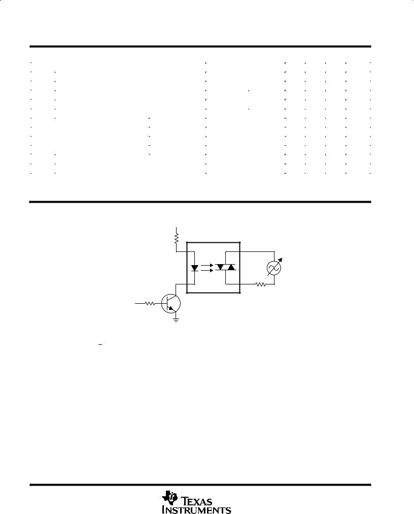
PARAMETER MEASUREMENT INFORMATION |
|||
|
VCC |
|
|
|
1 |
6 |
|
|
|
|
Vin = 30 V rms |
|
2 |
4 |
RL |
Input |
10 kΩ |
2N3904 |
|
|
|
||
(see Note A) |
|
|
|
|
|
|
|
NOTE A. The critical rate of rise of off-state voltage, dv/dt, is measured with the input set at 0 volts. The frequency of Vin is increased until the phototriac turns on. This frequency is then used to calculate the dv/dt according to the following formula:
dv dt + 2 2 p f Vin
The critical rate of rise of commutating voltage, dv/dt(c), is measured by applying occasional 5-volt pulses to the input and increasing the frequency of Vin until the phototriac remains on (latches) after the input pulse has ceased. With no further input pulses, the frequency of Vin is then gradually decreased until the phototriac turns off. The frequency at which turn-off occurs can then be used to calculate the dv/dt(c) according to the formula shown above.
Figure 1. Critical Rate of Rise Test Circuit
2 |
POST OFFICE BOX 655303 •DALLAS, TEXAS 75265 |

|
TIL3009, TIL3010, TIL3011, TIL3012 |
|
|
OPTOCOUPLERS/OPTOISOLATORS |
|
|
SOES027A ± DECEMBER 1987 ± REVISED APRIL 1998 |
|
|
|
|
TYPICAL CHARACTERISTICS |
||
EMITTING DIODE TRIGGER CURRENT (NORMALIZED) |
|
|
vs |
ON-STATE CHARACTERISTICS |
|
FREE-AIR TEMPERATURE |
||
Emitting Diode Trigger Current (Normalized)
1.4
1.3
1.2
1.1
1 |
|
|
|
|
|
|
0.9 |
|
|
|
|
|
|
0.8 |
|
|
|
|
|
|
± 50 |
± 25 |
0 |
25 |
50 |
75 |
100 |
TA ± Free-Air Temperature ± °C
|
800 |
Output tw = 80 μs |
|
|
|
|
|
|
|
|
|
|
|
||
|
600 |
IF = 20 mA |
|
|
|
|
|
|
f = 60 Hz |
|
|
|
|
|
|
± mA |
|
|
|
|
|
|
|
400 |
TA = 25°C |
|
|
|
|
|
|
Current |
200 |
|
|
|
|
|
|
|
|
|
|
|
|
|
|
On-State |
0 |
|
|
|
|
|
|
± 200 |
|
|
|
|
|
|
|
± Peak |
|
|
|
|
|
|
|
± 400 |
|
|
|
|
|
|
|
TM |
|
|
|
|
|
|
|
|
|
|
|
|
|
|
|
I |
± 600 |
|
|
|
|
|
|
|
|
|
|
|
|
|
|
|
± 800 |
|
|
|
|
|
|
|
± 3 |
± 2 |
± 1 |
0 |
1 |
2 |
3 |
VTM ± Peak On-State Voltage ± V
Figure 2 |
Figure 3 |
Off-State dv/dt ± V/ μs
CRITICAL RATE OF RISE OF OUTPUT VOLTAGE
OFF-STATE dv/dt AND COMMUTATING dv/dt(c) vs
LOAD RESISTANCE
14 |
|
|
|
|
|
|
|
|
|
|
|
|
|
0.24 |
|
|
TA = 25 |
|
°C |
|
|
|
|
|
|
|
|
||||
13 |
|
|
|
|
|
|
|
|
|
0.22 |
|
||||
|
See Figure 1 |
|
|
|
|
|
|
|
|
|
|||||
|
|
|
|
|
|
|
|
|
|
||||||
12 |
|
|
|
|
|
|
|
Off-State |
|
|
|
0.20 |
V/μ s |
||
|
|
|
|
|
|
|
|
|
|
||||||
|
|
|
|
|
|
|
|
|
|
|
|
|
|||
|
|
|
|
|
|
|
|
|
|
|
|
|
|||
11 |
|
|
|
|
|
|
|
|
|
|
|
|
|
0.18 |
|
|
|
|
|
|
|
|
|
|
|
|
|
|
± |
||
|
|
|
|
|
|
|
|
|
|
|
|
|
|
|
|
10 |
|
|
|
|
|
|
|
|
|
|
|
|
|
0.16 |
dv/dt(c) |
|
|
|
|
|
|
|
|
|
|
|
|
|
|
||
9 |
|
|
|
|
|
|
|
|
|
|
|
|
|
0.14 |
Commutating |
|
|
|
|
Commutating |
|
|
|
|
|
||||||
|
|
|
|
|
|
|
|
|
|
|
|||||
|
|
|
|
|
|
|
|
|
|
|
|
||||
8 |
|
|
|
|
|
|
|
|
|
|
|
|
|
0.12 |
|
|
|
|
|
|
|
|
|
|
|
|
|
|
|
||
|
|
|
|
|
|
|
|
|
|
|
|
|
|
||
7 |
|
|
|
|
|
|
|
|
|
|
|
|
|
0.10 |
|
|
|
|
|
|
|
|
|
|
|
|
|
|
|
||
6 |
|
|
|
|
|
|
|
|
|
|
|
|
|
0.08 |
|
|
|
|
|
|
|
|
|
|
|
|
|
|
|
||
5 |
|
|
|
|
|
|
|
|
|
|
dv/dt |
|
0.06 |
|
|
|
|
|
|
|
|
|
|
|
|
|
|
||||
|
|
|
|
|
|
|
|
|
|
dv/dt(c) |
|
|
|||
|
|
|
|
|
|
|
|
|
|
|
|
|
|
||
4 |
|
|
|
|
|
|
|
|
|
|
|
|
|
0.04 |
|
|
|
|
|
|
|
|
|
|
|
|
|
|
|
||
|
|
|
|
|
|
|
|
|
|
|
|
|
|
||
0 |
0.4 |
0.8 |
1.2 |
1.6 |
2 |
|
|||||||||
|
|
|
|
|
RL ± Load Resistance ± kΩ |
|
|
|
|||||||
Figure 4
POST OFFICE BOX 655303 •DALLAS, TEXAS 75265 |
3 |
 Loading...