


TPS767D325PWP
Texas Instruments TPS767D325PWP, TPS767D325PWPR, TPS767D318PWPR, TPS767D318PWP, TPS767D301PWPR Datasheet
...
TPS767D301, TPS767D318, TPS767D325
DUAL-OUTPUT LOW-DROPOUT VOLTAGE REGULATORS
SLVS209B – JULY 1999 – REVISED APRIL 2000
1
POST OFFICE BOX 655303 • DALLAS, TEXAS 75265
D
Dual Output Voltages for Split-Supply
Applications
D
Output Current Range of 0 mA to 1.0 A Per
Regulator
D
3.3-V/2.5-V, 3.3-V/1.8-V, and 3.3-V/Adjustable
Output
D
Fast-Transient Response
D
2% Tolerance Over Load and Temperature
D
Dropout Voltage Typically 350 mV at 1 A
D
Ultra Low 85 µA Typical Quiescent Current
D
1 µA Quiescent Current During Shutdown
D
Dual Open Drain Power-On Reset With
200-ms Delay for Each Regulator
D
28-Pin PowerP AD TSSOP Package
D
Thermal Shutdown Protection for Each
Regulator
description
The TPS767D3xx family of dual voltage regulators offers fast transient response, low dropout voltages and dual
outputs in a compact package and incorporating stability with 10-µF low ESR output capacitors.
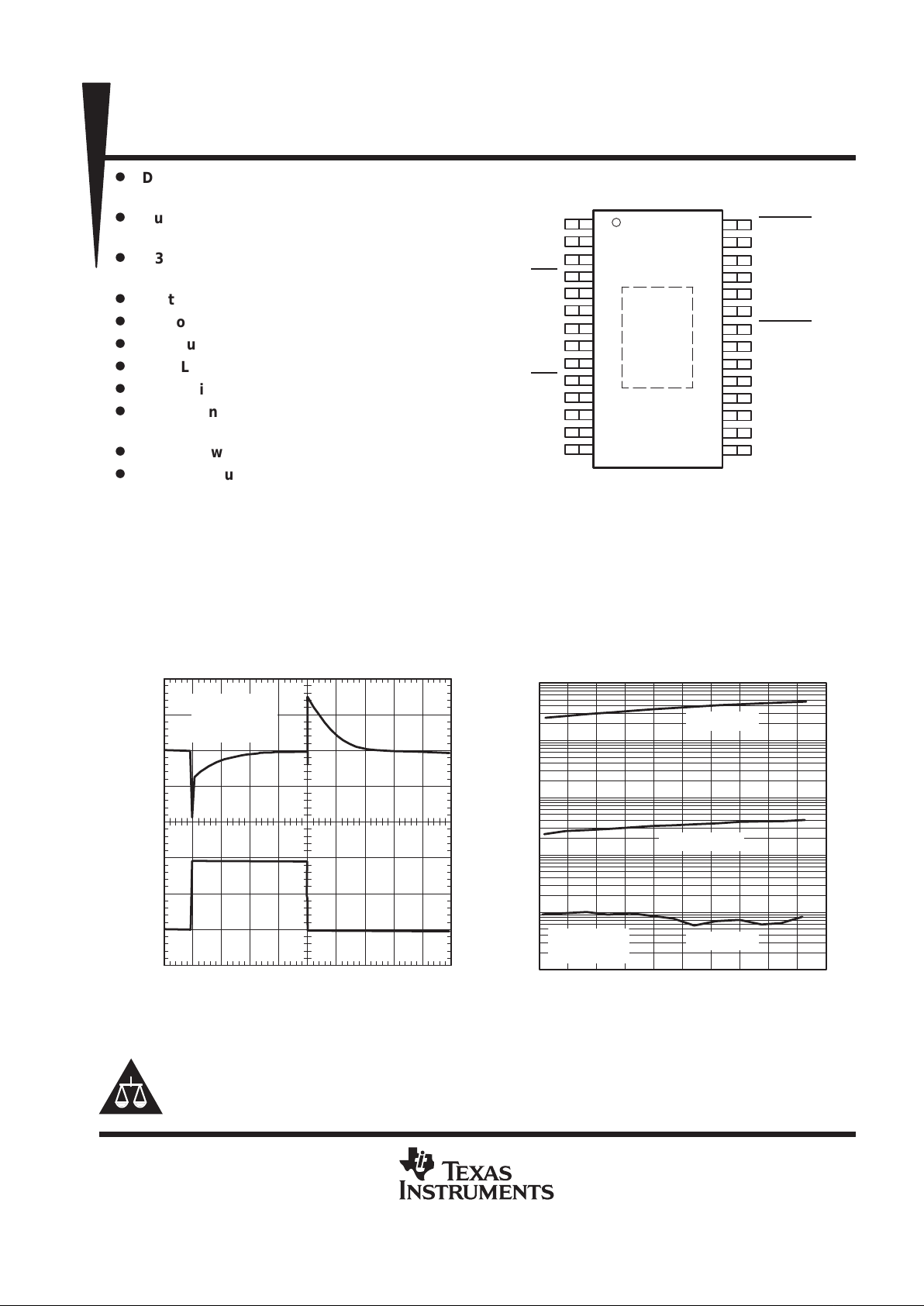
t – Time – µs
LOAD TRANSIENT RESPONSE
I – Output Current – A
O
V
O
– Change in∆
Output Voltage – mV
1
0.5
604020 80 100 140120 160 180 200
0
V
O
= 3.3 V
C
L
=100 µF
T
A
= 25°C
0
0
50
100
–50
–100
T
A
– Free-Air Temperature – °C
–40 0 20 120
10
3
–60 40 60 80 100
– Dropout Voltage – mV
V
DO
DROPOUT VOLTAGE
vs
FREE-AIR TEMPERATURE
10
2
10
1
10
0
10
–1
10
–2
–20 140
I
O
= 1 A
I
O
= 10 mA
I
O
= 0
V
O
= 3.3 V
C
O
= 10 µF
Copyright 2000, Texas Instruments Incorporated
PRODUCTION DATA information is current as of publication date.
Products conform to specifications per the terms of Texas Instruments
standard warranty. Production processing does not necessarily include
testing of all parameters.
Please be aware that an important notice concerning availability, standard warranty, and use in critical applications of
Texas Instruments semiconductor products and disclaimers thereto appears at the end of this data sheet.
PowerPAD is a trademark of Texas Instruments Incorporated.
1
2
3
4
5
6
7
8
9
10
11
12
13
14
28
27
26
25
24
23
22
21
20
19
18
17
16
15
NC
NC
1GND
1EN
1IN
1IN
NC
NC
2GND
2EN
2IN
2IN
NC
NC
1RESET
NC
NC
1FB/NC
1OUT
1OUT
2RESET
NC
NC
NC
2OUT
2OUT
NC
NC
PWP PACKAGE
(TOP VIEW)
NC – No internal connection
TPS767D301, TPS767D318, TPS767D325
DUAL-OUTPUT LOW-DROPOUT VOLTAGE REGULATORS
SLVS209B – JULY 1999 – REVISED APRIL 2000
2
POST OFFICE BOX 655303 • DALLAS, TEXAS 75265
description (continued)
The TPS767D3xx family of dual voltage regulators is designed primarily for DSP applications. These devices
can be used in any mixed-output voltage application, with each regulator supporting up to 1 A. Dual active-low
reset signals allow resetting of core-logic and I/O separately.
Because the PMOS device behaves as a low-value resistor, the dropout voltage is very low (typically 350 mV
at an output current of 1 A for the TPS767D325) and is directly proportional to the output current. Additionally ,
since the PMOS pass element is a voltage-driven device, the quiescent current is very low and independent
of output loading (typically 85 µA over the full range of output current, 0 mA to 1 A). These two key specifications
yield a significant improvement in operating life for battery-powered systems. This LDO family also features a
sleep mode; applying a TTL high signal to EN
(enable) shuts down the regulator, reducing the quiescent current
to 1 µA at T
J
= 25°C.
The RESET
output of the TPS767D3xx initiates a reset in microcomputer and microprocessor systems in the
event of an undervoltage condition. An internal comparator in the TPS767D3xx monitors the output voltage of
the regulator to detect an undervoltage condition on the regulated output voltage.
The TPS767D3xx is offered in 1.8-V, 2.5-V, and 3.3-V fixed-voltage versions and in an adjustable version
(programmable over the range of 1.5 V to 5.5 V). Output voltage tolerance is specified as a maximum of 2%
over line, load, and temperature ranges. The TPS767D3xx family is available in 28 pin PWP TSSOP package.
They operate over a junction temperature range of –40°C to 125°C.
AVAILABLE OPTIONS
T
A
REGULATOR 1
V
O
(V)
REGULATOR 2
V
O
(V)
TSSOP
(PWP)
Adj (1.5 – 5.5 V) 3.3 V TPS767D301PWP
–40°C to 125°C
1.8 V 3.3 V TPS767D318PWP
2.5 V 3.3 V TPS767D325PWP
The TPS767D301 is adjustable using an external resistor divider (see application
information). The PWP packages are available taped and reeled. Add an R suffix
to the device type (e.g., TPS767D301PWPR).
RESET
OUT
OUT
6
5
4
IN
IN
EN
GND
3
28
24
23
V
I
C1
0.1 µF
50 V
RESET
V
O
10 µF
+
TPS767D3xx
C
O
250 kΩ
Figure 1. Typical Application Circuit (Fixed Versions) for Single Channel
TPS767D301, TPS767D318, TPS767D325
DUAL-OUTPUT LOW-DROPOUT VOLTAGE REGULATORS
SLVS209B – JULY 1999 – REVISED APRIL 2000
3
POST OFFICE BOX 655303 • DALLAS, TEXAS 75265
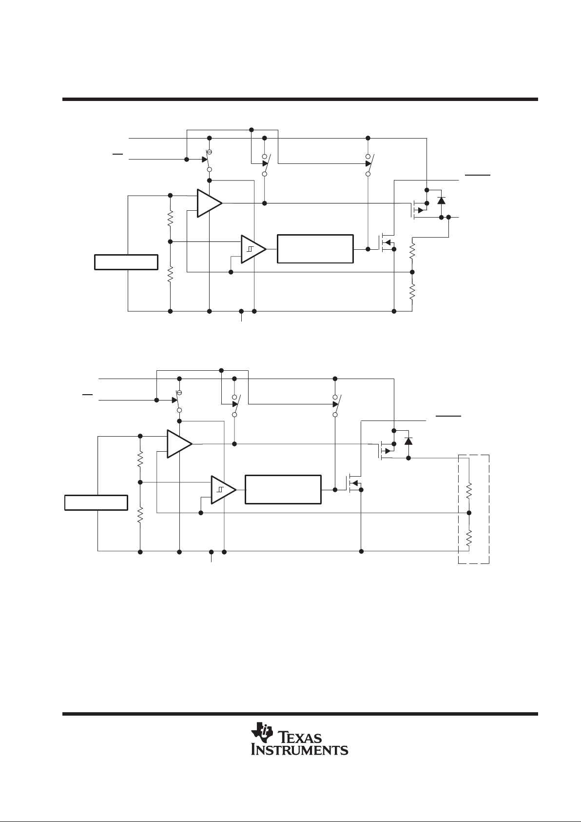
functional block diagram—adjustable version (for each LDO)
_
+
V
ref
= 1.1834 V
OUT
EN
GND
R1
R2
RESET
_
+
IN
200 ms Delay
functional block diagram—fixed-voltage version (for each LDO)
200 ms Delay
_
+
V
ref
= 1.1834 V
OUT
FB/NC
EN
GND
RESET
_
+
IN
External to the device
R1
R2
TPS767D301, TPS767D318, TPS767D325
DUAL-OUTPUT LOW-DROPOUT VOLTAGE REGULATORS
SLVS209B – JULY 1999 – REVISED APRIL 2000
4
POST OFFICE BOX 655303 • DALLAS, TEXAS 75265
Terminal Functions
TERMINAL
NAME NO.
I/O
DESCRIPTION
1GND 3 Regulator #1 ground
1EN 4 I Regulator #1 enable
1IN 5, 6 I Regulator #1 input supply voltage
2GND 9 Regulator #2 ground
2EN 10 I Regulator #2 enable
2IN 11, 12 I Regulator #2 input supply voltage
2OUT 17, 18 O Regulator #2 output voltage
2RESET 22 O Regulator #2 reset signal
1OUT 23, 24 O Regulator #1 output voltage
1FB/NC 25 I Regulator #1 output voltage feedback for adjustable and no connect for fixed output
1RESET 28 O Regulator #1 reset signal
NC 1, 2, 7, 8,
13–16, 19, 20,
21, 26, 27
No connection
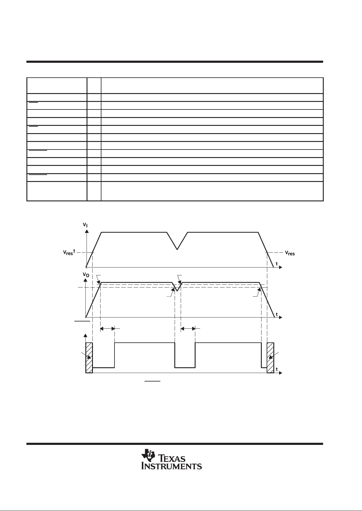
timing diagram
†
V
res
is the minimum input voltage for a valid RESET
. The symbol V
res
is not currently listed within EIA or JEDEC standards
for semiconductor symbology.
V
I
V
res
†
V
res
t
t
t
V
O
Threshold
Voltage
RESET
Output
200 ms
Delay
200 ms
Delay
Output
Undefined
Output
Undefined
V
IT+
‡
V
IT–
V
IT–
V
IT+
‡
Less than 5% of the
output voltage
‡
VIT –Trip voltage is typically 5% lower than the output voltage (95%V
O
)
TPS767D301, TPS767D318, TPS767D325
DUAL-OUTPUT LOW-DROPOUT VOLTAGE REGULATORS
SLVS209B – JULY 1999 – REVISED APRIL 2000
5
POST OFFICE BOX 655303 • DALLAS, TEXAS 75265
absolute maximum ratings over operating free-air temperature (unless otherwise noted)
†
Input voltage range
‡
, V
I
–0.3 V to 13.5 V. . . . . . . . . . . . . . . . . . . . . . . . . . . . . . . . . . . . . . . . . . . . . . . . . . . . . . . . . .
Input voltage range, V
I
(1IN, 2IN, EN) –0.3 V to V
I
+ 0.3 V. . . . . . . . . . . . . . . . . . . . . . . . . . . . . . . . . . . . . . . . . . .
Output voltage, V
O
(1OUT, 2OUT) 7 V. . . . . . . . . . . . . . . . . . . . . . . . . . . . . . . . . . . . . . . . . . . . . . . . . . . . . . . . . . . .
Output voltage, V
O
(RESET) 16.5 V. . . . . . . . . . . . . . . . . . . . . . . . . . . . . . . . . . . . . . . . . . . . . . . . . . . . . . . . . . . . . .
Peak output current Internally limited. . . . . . . . . . . . . . . . . . . . . . . . . . . . . . . . . . . . . . . . . . . . . . . . . . . . . . . . . . . . . .
ESD rating, HBM 2 kV. . . . . . . . . . . . . . . . . . . . . . . . . . . . . . . . . . . . . . . . . . . . . . . . . . . . . . . . . . . . . . . . . . . . . . . . . .
Continuous total power dissipation See dissipation rating tables. . . . . . . . . . . . . . . . . . . . . . . . . . . . . . . . . . . . . .
Operating virtual junction temperature range, T
J
–40°C to 125°C. . . . . . . . . . . . . . . . . . . . . . . . . . . . . . . . . . . . .
Storage temperature range, T
stg
–65°C to 150°C. . . . . . . . . . . . . . . . . . . . . . . . . . . . . . . . . . . . . . . . . . . . . . . . . . .
†
Stresses beyond those listed under “absolute maximum ratings” may cause permanent damage to the device. These are stress ratings only, and
functional operation of the device at these or any other conditions beyond those indicated under “recommended operating conditions” is not
implied. Exposure to absolute-maximum-rated conditions for extended periods may affect device reliability.
‡
All voltage values are with respect to network terminal ground.
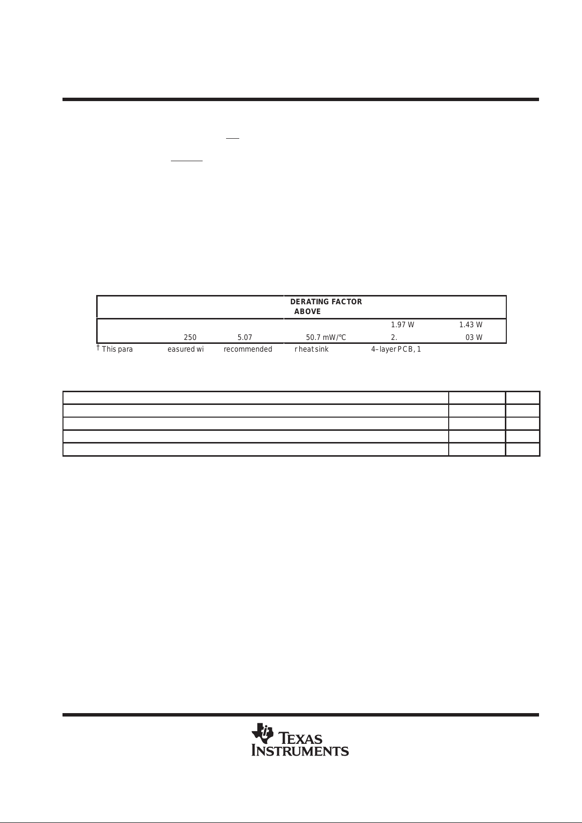
DISSIPATION RATING TABLE
PACKAGE
AIR FLOW
(CFM)
T
A
≤ 25°C
POWER RATING
БББББ
Á
DERATING FACTOR
ABOVE T
A
= 25°C
T
A
= 70°C
POWER RATING
T
A
= 85°C
POWER RATING
0
3.58 W
35.8 mW/°C
1.97 W
1.43 W
PWP
†
250 5.07 W
50.7 mW/°C 2.79 W 2.03 W
†
This parameter is measured with the recommended copper heat sink pattern on a 4–layer PCB, 1 oz. copper on 4–in x 4–in
ground layer. For more information, refer to TI technical brief literature number SLMA002.
recommended operating conditions
MIN MAX UNIT
Input voltage, V
I
#
(1IN, 2IN)
2.7 10 V
Output current for each LDO, I
O
(Note 1) 0 1.0 A
Output voltage range, V
O
(1OUT, 2OUT) 1.5 5.5 V
Operating virtual junction temperature, T
J
–40 125 °C
#
To calculate the minimum input voltage for your maximum output current, use the following equation: V
I(min)
= V
O(max)
+ V
DO(max
load)
.
NOTE 1: Continuous current and operating junction temperature are limited by internal protection circuitry, but it is not recommended that the
device operate under conditions beyond those specified in this table for extended periods of time.
TPS767D301, TPS767D318, TPS767D325
DUAL-OUTPUT LOW-DROPOUT VOLTAGE REGULATORS
SLVS209B – JULY 1999 – REVISED APRIL 2000
6
POST OFFICE BOX 655303 • DALLAS, TEXAS 75265
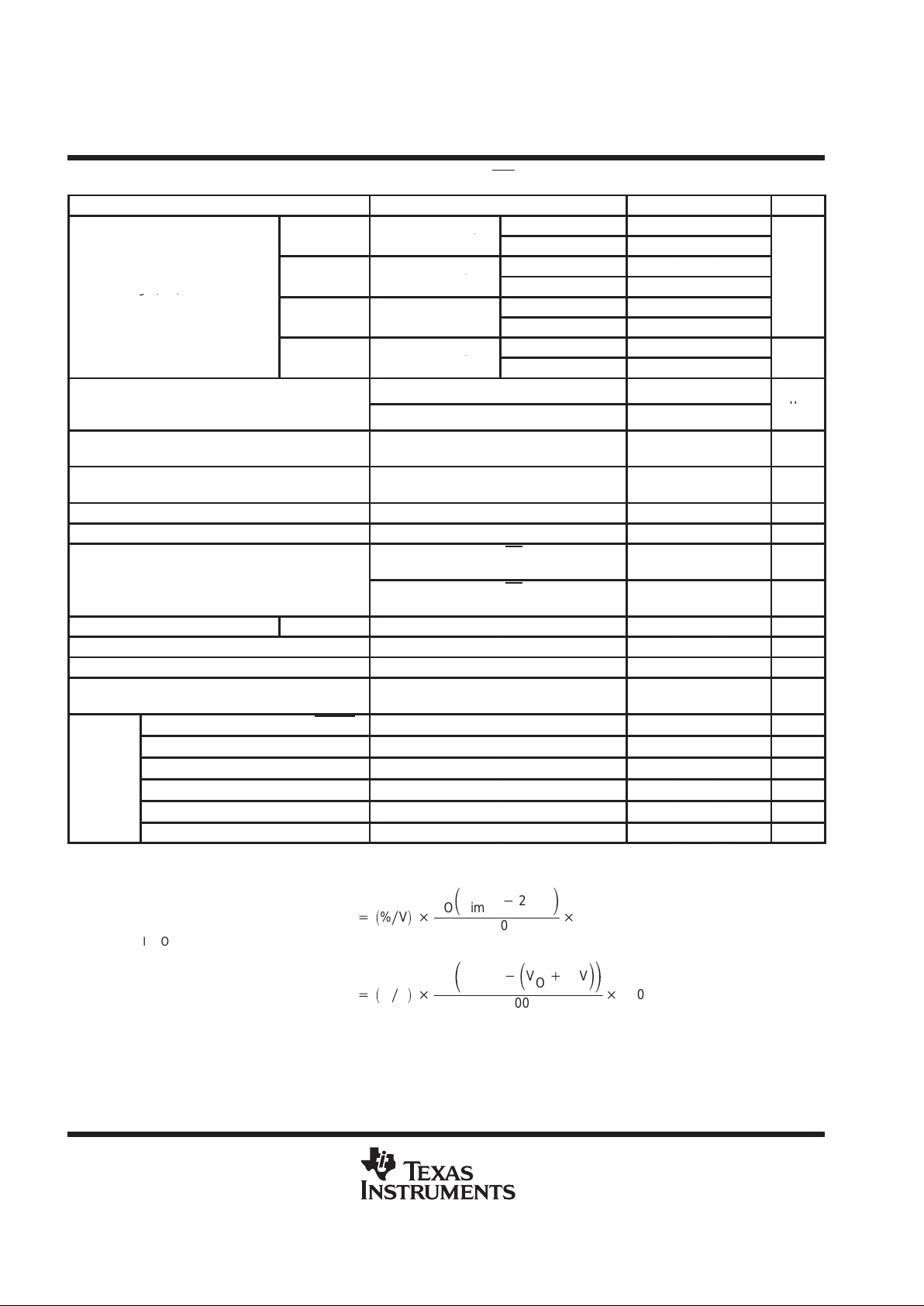
electrical characteristics, V
i
= V
O(nom)
+ 1 V , I
O
= 1 mA, EN = 0, C
O
= 10 µF(unless otherwise noted)
PARAMETER TEST CONDITIONS MIN TYP MAX UNIT
1.5 V ≤ V
≤ 5.5 V,
T
J
= 25°C V
O
Adj
u
stable
O
,
10 µA < I
O
< 1 A
T
J
= –40°C to 125°C 0.98V
O
1.02V
O
p
2.8 V < V
< 10 V,
T
J
= 25°C 1.8
Output voltage (V
)
1
.
8
V
O
u
p
u
t
I
,
10 µA < I
O
< 1 A
T
J
= –40°C to 125°C 1.764 1.836
V
g(
O
)
(see Note 2)
p
3.5 V < V
< 10 V,
T
J
= 25°C 2.5
2
.
5
V
O
u
tp
u
t
I
,
10 µA < I
O
< 1 A
T
J
= –40°C to 125°C 2.45 2.55
p
4.3 V < V
< 10 V,
T
J
= 25°C 3.3
3
.
3
V
O
u
tp
u
t
I
,
10 µA < I
O
< 1 A
T
J
= –40°C to 125°C 3.234 3.366
V
Quiescent current (GND current) for each LDO
10 µA < I
O
< 1 A, T
J
= 25°C 85
(
see
N
o
t
e
2)
I
O
= 1 A, T
J
= –40°C to 125°C 125
µ
A
Output voltage line regulation for each LDO
(∆V
O
/V
O
)
(see Notes 2 and 3)
V
O
+ 1 V < V
I
≤ 10 V, T
J
= 25°C 0.01 %/V
Output noise voltage
BW = 300 Hz to 50 kHz,
C
O
= 10 µF, T
J
= 25°C
190 µVrms
Output current Limit for each LDO V
O
= 0 V 1.7 2 A
Thermal shutdown juction temperature 150 °C
2.7 < V
I
< 10V ,
T
J
= 25°C,
EN = V
I,
1 µA
Standb
y
c
u
rrent
for
each
LDO
2.7 < V
I
< 10V ,
T
J
= –40°C to 125°C
EN = V
I,
10 µA
FB input current Adjustable FB = 1.5 V 2 nA
High level enable input voltage 2.0 V
Low level enable input voltage 0.8 V
Power supply ripple rejection (see Note 2)
f = 1 KHz,
T
J
= 25°C,
C
O
= 10 µF
60 dB
Minimum input voltage for valid RESET I
O(RESET)
= 300µA 1.1 V
Trip threshold voltage V
O
decreasing 92 98 %V
O
Hysteresis voltage Measured at V
O
0.5 %V
O
Reset
Output low voltage V
I
= 2.7 V, I
O(RESET)
= 1 mA 0.15 0.4 V
Leakage current V
(RESET)
= 7 V 1 µA
RESET time-out delay 200 mA
NOTES: 2. Minimum IN operating voltage is 2.7 V or V
O(typ)
+ 1 V, whichever is greater. maximum IN voltage 10V.
3. If VO ≤ 1.8 V, V
imin
= 2.7 V, and V
imax
= 10 V:
Line Reg. (mV)
+
ǒ
%
ń
V
Ǔ
V
O
ǒ
V
imax
*
2.7 V
Ǔ
100
1000
If VO ≥ 2.5 V, V
imin
= Vo + 1 V, and V
imax
= 10 V:
Line Reg. (mV)
+
ǒ
%
ń
V
Ǔ
V
O
ǒ
V
imax
*
ǒ
V
O
)
1V
Ǔ
Ǔ
100
1000
 Loading...