


 Loading...
TEXAS INSTRUMENTS TPS79301, TPS79318, TPS79325, TPS79328, TPS793285 Technical data
...
|
|
|
TPS79301, TPS79318 |
|
|
|
TPS79325, TPS79328, TPS793285 |
|
|
|
|
www.ti.com |
|
|
TPS79330, TPS79333, TPS793475 |
|
|
SLVS348H –JULY 2001 –REVISED OCTOBER 2004 |
|
|
|
|
ULTRALOW-NOISE, HIGH PSRR, FAST RF 200-mA LOW-DROPOUT LINEAR REGULATORS IN NanoStar™ WAFER CHIP SCALE AND SOT23
FEATURES
∙200-mA RF Low-Dropout Regulator With Enable
∙Available in 1.8-V, 2.5-V, 2.8-V, 2.85-V, 3-V, 3.3-V, 4.75-V, and Adjustable (1.22-V to 5.5-V)
∙High PSRR (70 dB at 10 kHz)
∙Ultralow-Noise (32 µV RMS, TPS79328)
∙Fast Start-Up Time (50 µs)
∙Stable With a 2.2-µF Ceramic Capacitor
∙Excellent Load/Line Transient Response
∙Very Low Dropout Voltage (112 mV at Full Load, TPS79330)
∙5- and 6-Pin SOT23 (DBV) and NanoStar Wafer Chip Scale (YEQ) Packages
APPLICATIONS
∙RF: VCOs, Receivers, ADCs
∙Audio
∙Cellular and Cordless Telephones
∙ Bluetooth™, Wireless LAN
∙Handheld Organizers, PDAs
DESCRIPTION
The TPS793xx family of low-dropout (LDO) low-power linear voltage regulators features high power-supply rejection ratio (PSRR), ultralow-noise, fast start-up, and excellent line and load transient responses in NanoStar wafer chip scale and SOT23 packages. NanoStar packaging gives an ultrasmall footprint as well as an ultralow profile and package weight, making it ideal for portable applications such as handsets and PDAs. Each device in the family is stable, with a small 2.2-µF ceramic capacitor on the output. The TPS793xx family uses an advanced, proprietary BiCMOS fabrication process to yield extremely low dropout voltages (e.g., 112 mV at 200 mA, TPS79330). Each device achieves fast start-up times (approximately 50 µs with a 0.001-µF bypass capacitor) while consuming very low quiescent current (170 µA typical). Moreover, when the device is placed in standby mode, the supply current is reduced to less than 1 µA. The TPS79328 exhibits approximately 32 µVRMS of output voltage noise at 2.8-V output with a 0.1-µF bypass capacitor. Applications with analog components that are noise-sensitive, such as portable RF electronics, benefit from the high PSRR and low-noise features as well as the fast response time.
|
DBV PACKAGE |
|
|
|
|
|
||
|
(TOP VIEW) |
|
|
|
TPS79328 |
|
||
IN |
1 |
5 |
OUT |
|
|
|
||
|
OUTPUT SPECTRAL NOISE DENSITY |
|||||||
|
|
|
|
|
||||
GND |
2 |
|
|
|
|
|
vs |
|
|
|
|
|
|
FREQUENCY |
|
||
|
3 |
4 |
|
|
0.30 |
|
||
EN |
NR |
√Hz) |
|
|
|
|||
|
|
|
|
VIN = 3.8 V |
|
|||
|
Fixed Option |
|
|
|
|
|||
|
|
|
|
COUT = 2.2 μF |
|
|||
|
|
|
|
V/(μ |
0.25 |
|
|
|
|
|
|
|
|
CNR = 0.1 μF |
|
||
|
|
|
|
|
|
|
|
|
|
DBV PACKAGE |
Density |
|
|
|
|
||
|
(TOP VIEW) |
|
0.20 |
|
|
|
||
|
|
|
|
|
|
|||
IN |
|
|
OUT |
|
|
|
|
|
1 |
6 |
Noise |
|
|
|
|
||
GND |
2 |
5 |
FB |
0.15 |
|
IOUT = 1 mA |
|
|
|
Adjustable Option |
Spectral |
|
|
IOUT = 200 mA |
|
||
EN |
3 |
4 |
NR |
|
0.10 |
|
|
|
|
|
Output |
|
|
|
|||
|
YEQ |
|
0.05 |
|
|
|
||
|
PACKAGE |
|
|
|
|
|
|
|
|
(TOP VIEW) |
|
0 |
|
|
|
||
|
IN |
|
OUT |
|
|
|
|
|
|
C1 |
|
100 |
1 k |
10 k |
100 k |
||
|
C3 |
|
|
|
Frequency (Hz) |
|
||
|
|
B2 |
NR |
|
|
|
||
|
A3 |
A1 |
GND |
|
|
|
|
|
|
EN |
|
|
|
|
|
|
|
TPS79328
RIPPLE REJECTION
|
|
|
|
vs |
|
|
|
|
|
|
FREQUENCY |
|
|
||
|
100 |
|
|
|
|
|
|
|
90 |
|
|
|
IOUT = 200 mA |
|
|
(dB) |
80 |
|
|
|
|
|
|
70 |
|
|
|
|
|
|
|
|
|
|
|
|
|
|
|
Rejection |
60 |
|
|
|
|
|
|
50 |
|
|
|
|
|
|
|
|
|
|
|
|
|
|
|
Ripple |
40 |
IOUT = 10 mA |
|
|
|
||
|
|
|
|
||||
30 |
|
|
|
|
|
|
|
|
20 |
VIN = 3.8 V |
|
|
|
|
|
|
|
|
|
|
|
||
|
10 |
COUT = 10 μF |
|
|
|
|
|
|
0 |
CNR = 0.01 μF |
|
|
|
|
|
|
|
|
|
|
|
|
|
|
10 |
100 |
1 k |
10 k |
100 k |
1 M |
10 M |
Frequency (Hz)
Figure 1.
Please be aware that an important notice concerning availability, standard warranty, and use in critical applications of Texas Instruments semiconductor products and disclaimers thereto appears at the end of this data sheet.
Bluetooth is a trademark of Bluetooth Sig, Inc.
NanoStar is a trademark of Texas Instruments.
UNLESS OTHERWISE NOTED this document contains PRO- |
Copyright © 2001–2004, Texas Instruments Incorporated |
DUCTION DATA information current as of publication date. Prod- |
|
ucts conform to specifications per the terms of Texas Instruments |
|
standard warranty. Production processing does not necessarily |
|
include testing of all parameters. |
|
TPS79301, TPS79318 |
|
|
TPS79325, TPS79328, TPS793285 |
|
|
TPS79330, TPS79333, TPS793475 |
www.ti.com |
|
SLVS348H –JULY 2001 –REVISED OCTOBER 2004 |
||
|
This integrated circuit can be damaged by ESD. Texas Instruments recommends that all integrated circuits be handled with appropriate precautions. Failure to observe proper handling and installation procedures can cause damage.
ESD damage can range from subtle performance degradation to complete device failure. Precision integrated circuits may be more susceptible to damage because very small parametric changes could cause the device not to meet its published specifications.
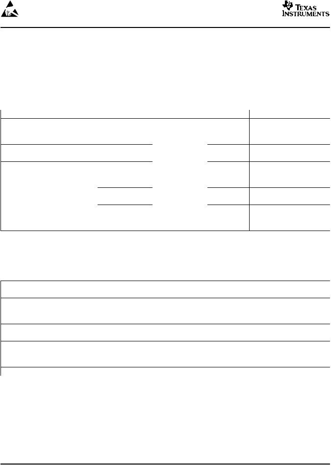
AVAILABLE OPTIONS(1) (2)
PRODUCT |
VOLTAGE |
PACKAGE |
TJ |
SYMBOL |
PART NUMBER |
|
TPS79301 |
1.22 V to 5.5 V |
SOT23 (DBV) |
|
PGVI |
TPS79301DBVR |
|
TPS79318 |
1.8 V |
SOT23 (DBV) |
|
PHHI |
TPS79318DBVR |
|
CSP (YEQ) |
|
E3 |
TPS79318YEQ |
|||
|
|
|
||||
TPS79325 |
2.5 V |
SOT23 (DBV) |
|
PGWI |
TPS79325DBVR |
|
CSP (YEQ) |
|
E4 |
TPS79325YEQ |
|||
|
|
|
||||
TPS79328 |
2.8 V |
SOT23 (DBV) |
|
PGXI |
TPS79328DBVR |
|
CSP (YEQ) |
-40°C to +125°C |
E2 |
TPS79328YEQ |
|||
|
|
|||||
TPS793285 |
2.85 V |
SOT23 (DBV) |
|
PHII |
TPS793285DBVR |
|
CSP (YEQ) |
|
E5 |
TPS793285YEQ |
|||
|
|
|
||||
TPS79330 |
3 V |
SOT23 (DBV) |
|
PGYI |
TPS79330DBVR |
|
CSP (YEQ) |
|
E6 |
TPS79330YEQ |
|||
|
|
|
||||
TPS79333 |
3.3 V |
SOT23 (DBV) |
|
PHUI |
TPS79333DBVR |
|
TPS793475 |
4.75 V |
SOT23 (DBV) |
|
PHJI |
TPS793475DBVR |
(1)For the most current package and ordering information, see the Package Option Addendum located at the end of this data sheet.
(2)DBVR indicates tape and reel of 3000 parts. YEQR indicates tape and reel of 3000 parts. YEQT indicates tape and reel of 250 parts.
ABSOLUTE MAXIMUM RATINGS
over operating temperature range (unless otherwise noted)(1)
|
UNIT |
VIN range |
-0.3 V to 6 V |
VEN range |
-0.3 V to VIN + 0.3 V |
VOUT range |
-0.3 V to 6 V |
Peak output current |
Internally limited |
ESD rating, HBM |
2 kV |
ESD rating, CDM |
500 V |
Continuous total power dissipation |
See Dissipation Ratings Table |
Junction temperature range, DBV package |
-40°C to 150°C |
Junction temperature range, YEQ package |
-40°C to 125°C |
Storage temperature range, Tstg |
-65°C to 150°C |
(1)Stresses beyond those listed under absolute maximum ratings may cause permanent damage to the device. These are stress ratings only, and functional operation of the device at these or any other conditions beyond those indicated under recommended operating conditions is not implied. Exposure to absolute-maximum-rated conditions for extended periods may affect device reliability.
2
|
|
|
|
|
|
TPS79301, TPS79318 |
|
|
|
|
|
|
TPS79325, TPS79328, TPS793285 |
||
www.ti.com |
|
|
|
TPS79330, TPS79333, TPS793475 |
|||
|
|
|
SLVS348H –JULY 2001 –REVISED OCTOBER 2004 |
||||
|
|
|
|
|
|||
DISSIPATION RATINGS TABLE |
|
|
|
|
|
||
|
|
|
|
DERATING FACTOR |
TA ≤ 25°C |
TA = 70°C |
TA = 85°C |
|
|
|
|
POWER |
POWER |
POWER |
|
BOARD |
PACKAGE |
RθJC |
RθJA |
ABOVE TA = 25°C |
RATING |
RATING |
RATING |
Low-K(1) |
DBV |
65°C/W |
255°C/W |
3.9 mW/°C |
390 mW |
215 mW |
155 mW |
High-K(2) |
DBV |
65°C/W |
180°C/W |
5.6 mW/°C |
560 mW |
310 mW |
225 mW |
Low-K(1) |
YEQ |
27°C/W |
255°C/W |
3.9 mW/°C |
390 mW |
215 mW |
155 mW |
High-K(2) |
YEQ |
27°C/W |
190°C/W |
5.3 mW/°C |
530 mW |
296 mW |
216 mW |
(1)The JEDEC low-K (1s) board design used to derive this data was a 3-inch x 3-inch, two layer board with 2 ounce copper traces on top of the board.
(2)The JEDEC high-K (2s2p) board design used to derive this data was a 3-inch x 3-inch, multilayer board with 1 ounce internal power and ground planes and 2 ounce copper traces on top and bottom of the board.
ELECTRICAL CHARACTERISTICS
over recommended operating temperature range TJ = -40 to 125°C, VEN = VIN, VIN = VOUT(nom) + 1 V(1), IOUT = 1 mA, COUT = 10 µF, CNR = 0.01 µF (unless otherwise noted). Typical values are at 25°C.
PARAMETER |
|
|
|
TEST CONDITIONS |
|
MIN |
TYP |
MAX |
UNIT |
|||||
V Input voltage(1) |
|
|
|
|
|
|
|
|
|
2.7 |
|
5.5 |
V |
|
IN |
|
|
|
|
|
|
|
|
|
|
|
|
|
|
IOUT Continuous output current |
|
|
|
|
|
|
|
0 |
|
200 |
mA |
|||
VFB Internal reference (TPS79301) |
|
|
|
|
|
|
|
1.201 |
1.225 |
1.250 |
V |
|||
Output voltage range (TPS79301) |
|
|
|
|
|
|
|
VFB |
|
5.5 - VDO |
V |
|||
|
|
|
TPS79318 |
0 |
µA < IOUT < 200 mA, |
2.8 V < VIN < 5.5 V |
1.764 |
1.8 |
1.836 |
V |
||||
|
|
|
TPS79325 |
0 |
µA < IOUT < 200 mA, |
3.5 V < VIN < 5.5 V |
2.45 |
2.5 |
2.55 |
V |
||||
|
|
|
TPS79328 |
0 |
µA < IOUT < 200 mA, |
3.8 V < VIN < 5.5 V |
2.744 |
2.8 |
2.856 |
V |
||||
Output voltage |
|
|
TPS793285 |
0 |
µA < IOUT < 200 mA, |
3.85 V < VIN < 5.5 V |
2.793 |
2.85 |
2.907 |
V |
||||
|
|
|
TPS79330 |
0 |
µA < IOUT < 200 mA, |
4 V < VIN < 5.5 V |
2.94 |
3 |
3.06 |
V |
||||
|
|
|
TPS79333 |
0 |
µA ≤ IOUT < 200 mA, |
4.3 V < VIN < 5.5 V |
3.234 |
3.3 |
3.366 |
V |
||||
|
|
|
TPS793475 |
0 |
µA < IOUT < 200 mA, |
5.25 V < VIN < 5.5 V |
4.655 |
4.75 |
4.845 |
V |
||||
Line regulation ( |
V %/ |
V |
) (1) |
V |
OUT |
+ 1 V < V |
IN |
≤ 5.5 V |
|
|
0.05 |
0.12 |
%/V |
|
|
OUT |
IN |
|
|
|
|
|
|
|
|
|
|||
Load regulation ( |
VOUT%/ |
IOUT) |
0 |
µA < IOUT < 200 mA, |
TJ = 25°C |
|
5 |
|
mV |
|||||
|
|
|
TPS79328 |
IOUT = 200 mA |
|
|
|
|
120 |
200 |
|
|||
Dropout voltage(2) |
|
TPS793285 |
IOUT = 200 mA |
|
|
|
|
120 |
200 |
|
||||
|
TPS79330 |
IOUT = 200 mA |
|
|
|
|
112 |
200 |
mV |
|||||
(VIN = VOUT(nom) - 0.1V) |
|
|
|
|
|
|||||||||
|
TPS79333 |
IOUT = 200 mA |
|
|
|
|
102 |
180 |
|
|||||
|
|
|
|
|
|
|
|
|||||||
|
|
|
TPS793475 |
IOUT = 200 mA |
|
|
|
|
77 |
125 |
|
|||
Output current limit |
|
|
VOUT = 0 V |
|
|
|
285 |
|
600 |
mA |
||||
GND pin current |
|
|
|
0 |
µA < IOUT < 200 mA |
|
|
170 |
220 |
µA |
||||
Shutdown current(3) |
|
|
V |
EN |
= 0 V, 2.7 V < V < 5.5 V |
|
0.07 |
1 |
µA |
|||||
|
|
|
|
|
|
|
|
IN |
|
|
|
|
|
|
FB pin current |
|
|
|
VFB = 1.8 V |
|
|
|
|
|
1 |
µA |
|||
|
|
|
|
f = 100 Hz, TJ = 25°C, |
IOUT = 10 mA |
|
70 |
|
|
|||||
Power-supply ripple rejection |
TPS79328 |
f = 100 Hz, TJ = 25°C, |
IOUT = 200 mA |
|
68 |
|
dB |
|||||||
f = 10 kHz, TJ = 25°C, |
IOUT = 200 mA |
|
70 |
|
||||||||||
|
|
|
|
|
|
|
||||||||
|
|
|
|
f = 100 kHz, TJ = 25°C, |
IOUT = 200 mA |
|
43 |
|
|
|||||
|
|
|
|
|
|
|
|
|
|
CNR = 0.001 µF |
|
55 |
|
|
Output noise voltage (TPS79328) |
BW = 200 Hz to 100 kHz, |
CNR = 0.0047 µF |
|
36 |
|
µVRMS |
||||||||
IOUT = 200 mA |
|
|
C = 0.01 µF |
|
33 |
|
||||||||
|
|
|
|
|
|
|
|
|
|
NR |
|
|
|
|
|
|
|
|
|
|
|
|
|
|
CNR = 0.1 µF |
|
32 |
|
|
(1)Minimum VIN is 2.7 V or VOUT + VDO, whichever is greater.
(2)Dropout is not measured for the TPS79318 and TPS79325 since minimum VIN = 2.7 V.
(3)For adjustable versions, this applies only after VIN is applied; then VEN transitions high to low.
3

TPS79301, TPS79318 |
|
|
TPS79325, TPS79328, TPS793285 |
|
|
TPS79330, TPS79333, TPS793475 |
www.ti.com |
|
SLVS348H –JULY 2001 –REVISED OCTOBER 2004 |
||
|
ELECTRICAL CHARACTERISTICS (continued)
over recommended operating temperature range TJ = -40 to 125°C, VEN = VIN, VIN = VOUT(nom) + 1 V, IOUT = 1 mA, COUT = 10 µF, CNR = 0.01 µF (unless otherwise noted). Typical values are at 25°C.
PARAMETER |
TEST CONDITIONS |
|
MIN |
TYP |
MAX |
UNIT |
|
|
CNR = 0.001 µF |
|
50 |
|
|
Time, start-up (TPS79328) |
RL = 14 Ω, COUT = 1 µF |
CNR = 0.0047 µF |
|
70 |
|
µs |
|
|
CNR = 0.01 µF |
|
100 |
|
|
High level enable input voltage |
2.7 V < VIN < 5.5 V |
|
1.7 |
|
VIN |
V |
Low level enable input voltage |
2.7 V < VIN < 5.5 V |
|
0 |
|
0.7 |
V |
EN pin current |
VEN = 0 |
|
-1 |
|
1 |
µA |
UVLO threshold |
VCC rising |
|
2.25 |
|
2.65 |
V |
UVLO hysteresis |
|
|
|
100 |
|
mV |
4

TPS79301, TPS79318
TPS79325, TPS79328, TPS793285
TPS79330, TPS79333, TPS793475
www.ti.com
SLVS348H –JULY 2001 –REVISED OCTOBER 2004
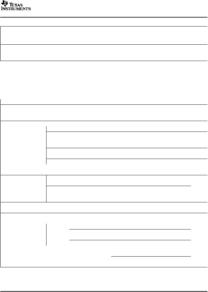
FUNCTIONAL BLOCK DIAGRAMS
ADJUSTABLE VERSION
IN 
 OUT
OUT
|
UVLO |
Current |
|
59 k |
|
|
2.45V |
Sense |
|
|
|
GND |
|
ILIM |
|
SHUTDOWN |
R1 |
|
|
_ |
+ |
|
|
|
|
|
FB |
||
|
|
|
|
||
|
|
|
|
|
|
EN |
|
|
|
|
R2 |
|
|
|
|
|
|
|
|
UVLO |
|
|
|
|
Thermal |
|
|
|
|
|
Shutdown |
QuickStart |
|
|
External to |
|
|
|
|
the Device |
|
|
|
|
|
|
|
|
Bandgap |
250 kΩ |
|
Vref |
|
IN |
Reference |
|
NR |
||
|
|
|
|||
|
1.22V |
|
|
|
|
FIXED VERSION
IN |
UVLO |
|
|
|
OUT |
|
Current |
|
|
|
|
|
2.45V |
|
|
|
|
|
|
Sense |
|
|
|
GND |
|
ILIM |
|
SHUTDOWN |
|
|
|
|
R1 |
|
|
|
|
|
_ |
|
|
|
|
|
+ |
|
|
EN |
|
|
|
|
|
|
|
|
|
|
|
|
|
UVLO |
|
|
|
|
|
|
|
R2 |
|
|
Thermal |
|
|
|
|
|
Shutdown |
QuickStart |
|
R2 = 40 kΩ |
|
|
|
|
|
||
|
Bandgap |
Ω |
|
Vref |
|
IN |
Reference |
250 k |
|
NR |
|
|
|
|
|||
|
1.22V |
|
|
|
|
|
|
|
|
Terminal Functions |
|
|
TERMINAL |
|
|
||
NAME |
SOT23 |
SOT23 |
WCSP |
DESCRIPTION |
|
ADJ |
FIXED |
FIXED |
|
||
|
|
||||
NR |
4 |
4 |
B2 |
Connecting an external capacitor to this pin bypasses noise generated by the internal bandgap. |
|
This improves power-supply rejection and reduces output noise. |
|||||
|
|
|
|
||
EN |
3 |
3 |
A3 |
Driving the enable pin (EN) high turns on the regulator. Driving this pin low puts the regulator into |
|
shutdown mode. EN can be connected to IN if not used. |
|||||
|
|
|
|
||
FB |
5 |
N/A |
N/A |
This terminal is the feedback input voltage for the adjustable device. |
|
GND |
2 |
2 |
A1 |
Regulator ground |
|
IN |
1 |
1 |
C3 |
Unregulated input to the device. |
|
OUT |
6 |
5 |
C1 |
Output of the regulator. |
|
5

TPS79301, TPS79318
TPS79325, TPS79328, TPS793285
TPS79330, TPS79333, TPS793475
www.ti.com
SLVS348H –JULY 2001 –REVISED OCTOBER 2004
TYPICAL CHARACTERISTICS (SOT23 PACKAGE)
TPS79328 |
TPS79328 |
OUTPUT VOLTAGE |
OUTPUT VOLTAGE |
vs |
vs |
OUTPUT CURRENT |
JUNCTION TEMPERATURE |
|
2.805 |
|
|
|
|
2.805 |
|
2.804 |
|
|
VIN = 3.8 V |
|
|
|
|
|
COUT = 10 μF |
|
|
|
|
|
|
|
|
2.800 |
|
|
2.803 |
|
|
TJ = 25°C |
|
|
|
|
|
|
|
||
|
2.802 |
|
|
|
|
2.795 |
|
|
|
|
|
|
|
(V) |
2.801 |
|
|
|
(V) |
|
|
|
|
|
|
||
OUT |
2.800 |
|
|
|
OUT |
2.790 |
|
|
|
|
|
||
V |
2.799 |
|
|
|
V |
|
|
|
|
|
|
|
|
|
2.798 |
|
|
|
|
2.785 |
|
|
|
|
|
|
|
|
2.797 |
|
|
|
|
2.780 |
|
2.796 |
|
|
|
|
|
|
|
|
|
|
|
|
|
2.795 |
50 |
100 |
150 |
200 |
2.775 |
|
0 |
|
IOUT (mA)
|
|
IOUT = 1 mA |
|
|
||
IOUT = 200 mA |
|
|
|
|||
VIN = 3.8 V |
|
|
|
|
|
|
COUT = 10 μF |
|
|
|
|
|
|
−40 −25 −10 5 |
20 |
35 |
50 |
65 |
80 |
95 110 125 |
|
|
TJ (°C) |
|
|
|
|
Figure 2. |
Figure 3. |
TPS79328
GROUND CURRENT vs
JUNCTION TEMPERATURE
|
250 |
|
|
|
|
|
|
|
VIN = 3.8 V |
|
|
|
|
|
|
|
COUT = 10 μF |
|
IOUT = 1 mA |
|
|||
|
200 |
|
|
|
|
|
|
(μA) |
150 |
|
IOUT = 200 mA |
|
|||
|
|
|
|
|
|
||
|
|
|
|
|
|
|
|
GND |
|
|
|
|
|
|
|
I |
100 |
|
|
|
|
|
|
|
|
|
|
|
|
|
|
|
50 |
|
|
|
|
|
|
|
0 |
|
|
|
|
|
|
|
−40 −25−10 5 |
20 |
35 |
50 |
65 |
80 |
95 110 125 |
|
|
|
TJ (°C) |
|
|
|
|
Figure 4.
TPS79328 OUTPUT SPECTRAL |
TPS79328 OUTPUT SPECTRAL |
NOISE DENSITY |
NOISE DENSITY |
vs |
vs |
FREQUENCY |
FREQUENCY |
Hz)V/(√μ |
0.30 |
|
|
|
Hz)V/(√μ |
0.30 |
|
|
|
|
|
VIN = 3.8 V |
|
|
|
VIN = 3.8 V |
|
||
|
0.25 |
|
COUT = 2.2 μF |
|
|
0.25 |
|
COUT = 10 μF |
|
|
|
CNR = 0.1 μF |
|
|
|
CNR = 0.1 μF |
|
||
Density |
|
|
|
Density |
|
|
|
||
0.20 |
|
|
|
0.20 |
|
|
|
||
Noise |
0.15 |
|
IOUT = 1 mA |
|
Noise |
0.15 |
|
IOUT = 1 mA |
|
|
|
|
|
|
|||||
Spectral |
|
|
|
Spectral |
|
|
|
||
0.10 |
|
IOUT = 200 mA |
|
0.10 |
|
IOUT = 200 mA |
|
||
Output |
0.05 |
|
|
|
Output |
0.05 |
|
|
|
|
|
|
|
|
|
|
|
||
|
0 |
|
|
|
|
0 |
|
|
|
|
100 |
1 k |
10 k |
100 k |
|
100 |
1 k |
10 k |
100 k |
|
|
Frequency (Hz) |
|
|
|
Frequency (Hz) |
|
||
TPS79328 OUTPUT SPECTRAL
NOISE DENSITY vs FREQUENCY
|
1.6 |
|
|
|
√Hz) |
1.4 |
|
VIN = 3.8 V |
|
|
IOUT = 200 mA |
|
||
(μV/ |
1.2 |
|
COUT = 10 μF |
|
Density |
CNR = 0.001 μF |
|
||
|
|
|||
1.0 |
|
μ |
|
|
|
CNR = 0.0047 F |
|
||
Noise |
0.8 |
|
CNR = 0.01 μF |
|
|
|
|
|
|
Spectral |
0.6 |
|
CNR = 0.1 μF |
|
0.4 |
|
|
|
|
Output |
0.2 |
|
|
|
|
|
|
|
|
|
0 |
|
|
|
|
100 |
1 k |
10 k |
100 k |
Frequency (Hz)
Figure 5. |
Figure 6. |
Figure 7. |
ROOT MEAN SQUARE OUTPUT
NOISE vs CNR
|
60 |
|
|
|
|
|
VOUT = 2.8 V |
||
|
50 |
IOUT = 200 mA |
||
) |
COUT = 10 |
μF |
||
|
||||
RMS |
|
|
|
|
(V |
40 |
|
|
|
Noise |
30 |
|
|
|
Output |
|
|
||
20 |
|
|
||
RMS, |
|
|
||
10 |
|
|
||
|
|
|
||
|
BW = 100 Hz to 100 kHz |
|
||
|
0 |
|
|
|
|
0.001 |
0.01 |
0.1 |
|
|
|
CNR (μF) |
|
|
Figure 8.
|
|
|
|
|
|
|
|
|
TPS79328 |
|
|
|
OUTPUT IMPEDANCE |
|
|
|
DROPOUT VOLTAGE |
||||||
|
|
|
vs |
|
|
|
|
|
vs |
|
|
|
|
FREQUENCY |
|
|
|
|
JUNCTION TEMPERATURE |
||||
2.5 |
VIN = 3.8 V |
|
|
|
|
|
180 |
VIN = 2.7 V |
|
|
|
|
|
|
|
|
|
|
|
|
|
||
|
COUT = 10 μF |
|
|
|
|
160 |
COUT = 10 |
μ |
|
|
|
|
TJ = 25° C |
|
|
|
|
|
|
F |
|
|
|
2.0 |
|
|
|
|
|
140 |
|
|
|
|
|
|
|
|
|
|
|
|
|
|
|
||
1.5 |
|
|
|
|
|
|
120 |
|
IOUT = 200 mA |
|
|
|
|
|
|
|
(mV) |
|
|
|
|||
(Ω) |
IOUT = 1 mA |
|
|
|
100 |
|
|
|
|
||
ZO |
|
|
|
|
|
DO |
80 |
|
|
|
|
1.0 |
|
|
|
|
|
V |
|
|
|
|
|
|
|
|
|
|
|
|
|
|
|
||
IOUT = 100 mA |
|
|
|
|
|
|
|
|
|
||
|
|
|
|
|
60 |
|
|
|
|
||
0.5 |
|
|
|
|
|
|
40 |
|
|
|
|
|
|
|
|
|
|
|
20 |
|
IOUT = 10 mA |
|
|
|
|
|
|
|
|
|
|
|
|
|
|
0 |
100 |
1 k |
10 k 100 k |
1 M |
10 M |
|
0 |
|
20 35 50 65 |
80 |
95 110 125 |
10 |
|
−40 −25−10 5 |
|||||||||
|
|
Frequency (Hz) |
|
|
|
|
|
TJ (°C) |
|
|
|
|
|
|
Figure 9. |
|
|
|
|
|
Figure 10. |
|
|
6
Loading...