


TPS76428DBVT
Texas Instruments TPS76428DBVT, TPS76428DBV, TPS76428DBVR, TPS76427DBVT, TPS76427DBVR Datasheet
...
TPS76425, TPS76427, TPS76428, TPS76430, TPS76433
LOW-POWER LOW-NOISE 150-mA LOW-DROPOUT LINEAR REGULATORS
SLVS180A – MARCH 1999 – REVISED JUNE 1999
1
POST OFFICE BOX 655303 • DALLAS, TEXAS 75265
D
150-mA Low Noise, Low-Dropout Regulator
D
Output Voltage: 2.5 V, 2.7 V, 2.8 V, 3.0 V, 3.3 V
D
Output Noise Typically 50 µV
D
Quiescent Current Typically 85 µA
D
Dropout Voltage, Typically 300 mV
at 150 mA
D
Thermal Protection
D
Over Current Limitation
D
Less Than 2-µA Quiescent Current in
Shutdown Mode
D
–40°C to 125°C Operating Junction
T emperature Range
D
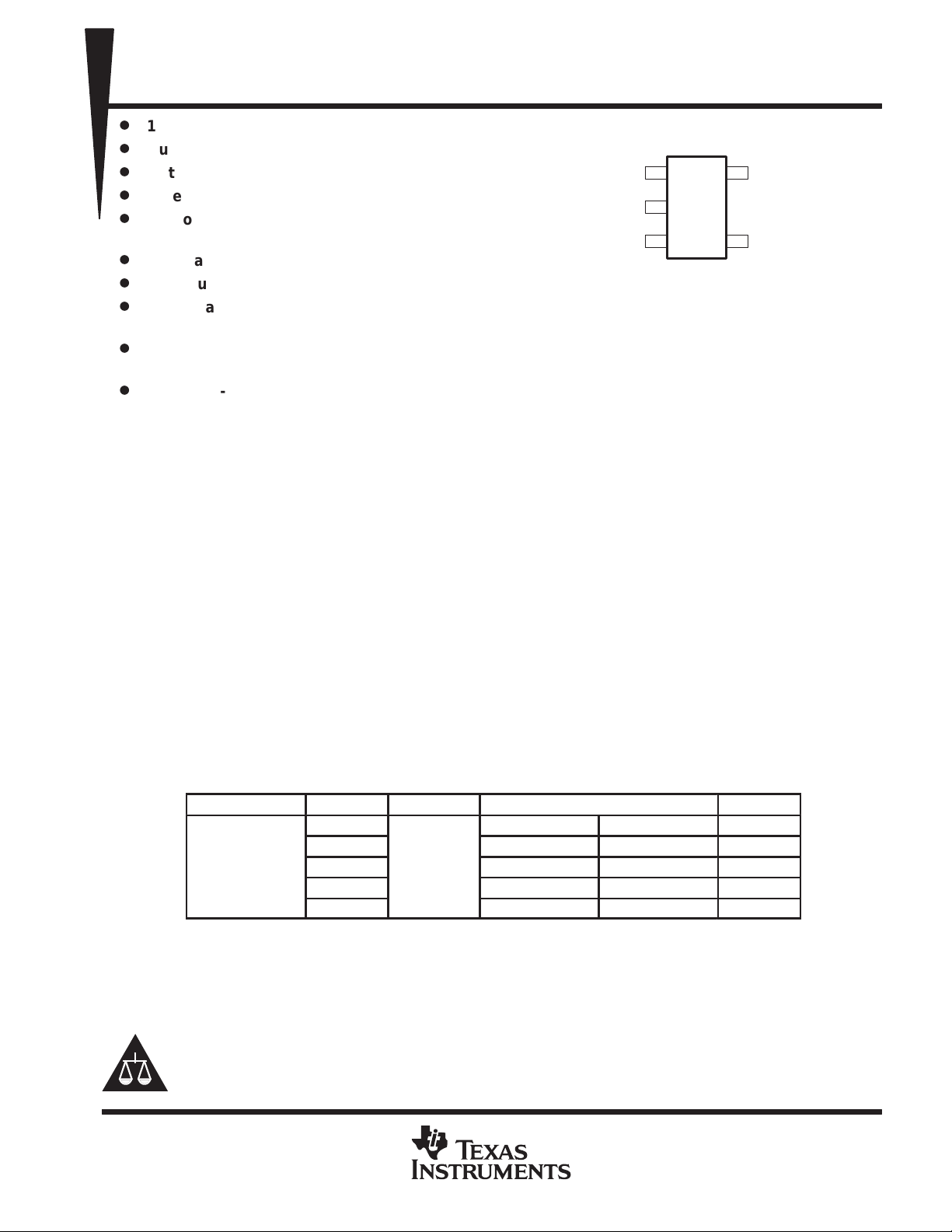
5-Pin SOT-23 (DBV) Package
description
The TPS764xx family of low-dropout (LDO) voltage regulators offers the benefits of a low noise, low-dropout
voltage, low-power operation, and miniaturized package. Additionally , they feature low quiescent current when
compared to conventional LDO regulators. Offered in 5-terminal small outline integrated-circuit SOT-23
package, the TPS764xx series devices are ideal for low-noise applications, cost-sensitive designs and
applications where board space is at a premium.
A combination of new circuit design and process innovation has enabled the usual pnp pass transistor to be
replaced by a PMOS pass element. Because the PMOS pass element behaves as a low-value resistor, the
dropout voltage is very low—typically 300 mV at 150 mA of load current (TPS76433)—and is directly
proportional to the load current. Since the PMOS pass element is a voltage-driven device, the quiescent current
is very low (140 µA maximum) and is stable over the entire range of output load current (0 mA to 150 mA).
Intended for use in portable systems such as laptops and cellular phones, the low-dropout voltage feature and
low-power operation result in a significant increase in system battery operating life.
The TPS764xx also features a logic-enabled sleep mode to shut down the regulator, reducing quiescent current
to 1 µA maximum at T
J
= 25°C.The TPS764xx is offered in 2.5-V , 2.7-V, 2.8-V , 3.0-V, and 3.3-V fixed-voltages.
AVAILABLE OPTIONS
T
J
VOLTAGE PACKAGE PART NUMBER SYMBOL
2.5 V TPS76425DBVT
†
TPS76425DBVR
‡
PBJI
2.7 V
TPS76427DBVT
†
TPS76427DBVR
‡
PBKI
–40°C to 125°C
2.8 V
SOT-23
TPS76428DBVT
†
TPS76428DBVR
‡
PCEI
3.0 V
(DBV)
TPS76430DBVT
†
TPS76430DBVR
‡
PBLI
3.3 V TPS76433DBVT
†
TPS76433DBVR
‡
PBMI
†
The DBVT passive indicates tape and reel of 250 parts.
‡
The DBVR passive indicates tape and reel of 3000 parts.
Copyright 1999, Texas Instruments Incorporated
PRODUCTION DATA information is current as of publication date.
Products conform to specifications per the terms of Texas Instruments
standard warranty. Production processing does not necessarily include
testing of all parameters.
Please be aware that an important notice concerning availability, standard warranty, and use in critical applications of
Texas Instruments semiconductor products and disclaimers thereto appears at the end of this data sheet.
3
2
4
5
DBV PACKAGE
(TOP VIEW)
1
IN
GND
EN
OUT
BYPASS
TPS76425, TPS76427, TPS76428, TPS76430, TPS76433
LOW-POWER LOW-NOISE 150-mA LOW-DROPOUT LINEAR REGULATORS
SLVS180A – MARCH 1999 – REVISED JUNE 1999
2
POST OFFICE BOX 655303 • DALLAS, TEXAS 75265
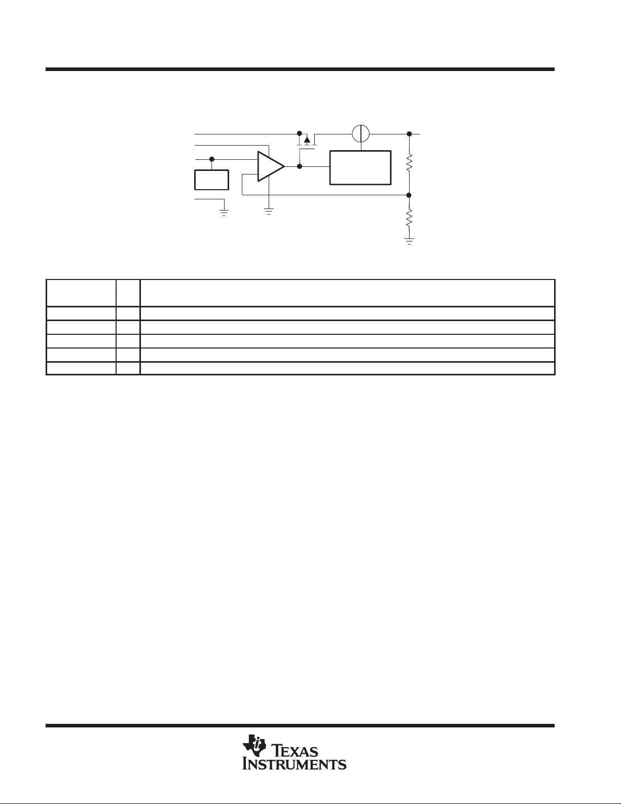
functional block diagram
TPS76425/ 27/ 28/ 30/ 33
OUT
IN
GND
EN
V
REF
Current Limit
/ Thermal
Protection
BYPASS
Terminal Functions
TERMINAL
NAME
I/O
DESCRIPTION
GND Ground
EN I Enable input
BYPASS Output bypass capacitor
IN I Input supply voltage
OUT O Regulated output voltage
TPS76425, TPS76427, TPS76428, TPS76430, TPS76433
LOW-POWER LOW-NOISE 150-mA LOW-DROPOUT LINEAR REGULATORS
SLVS180A – MARCH 1999 – REVISED JUNE 1999
3
POST OFFICE BOX 655303 • DALLAS, TEXAS 75265
absolute maximum ratings over operating free-air temperature range (unless otherwise noted)
Ĕ
Input voltage range
(see Note 1)
–0.3 V to 10 V. . . . . . . . . . . . . . . . . . . . . . . . . . . . . . . . . . . . . . . . . . . . . . . . . . . .
Voltage range at EN –0.3 V to V
I
+ 0.3 V. . . . . . . . . . . . . . . . . . . . . . . . . . . . . . . . . . . . . . . . . . . . . . . . . . . . . . . . . . .
Voltage on OUT, 7 V. . . . . . . . . . . . . . . . . . . . . . . . . . . . . . . . . . . . . . . . . . . . . . . . . . . . . . . . . . . . . . . . . . . . . . . . . . . . .
Peak output current Internally limited. . . . . . . . . . . . . . . . . . . . . . . . . . . . . . . . . . . . . . . . . . . . . . . . . . . . . . . . . . . . . .
ESD rating, HBM 2 kV. . . . . . . . . . . . . . . . . . . . . . . . . . . . . . . . . . . . . . . . . . . . . . . . . . . . . . . . . . . . . . . . . . . . . . . . . .
Continuous total power dissipation See dissipation rating tables. . . . . . . . . . . . . . . . . . . . . . . . . . . . . . . . . . . . . .
Operating virtual junction temperature range, T
J
–40°C to 150°C. . . . . . . . . . . . . . . . . . . . . . . . . . . . . . . . . . . . .
Storage temperature range, T
stg
–65°C to 150°C. . . . . . . . . . . . . . . . . . . . . . . . . . . . . . . . . . . . . . . . . . . . . . . . . . .
†
Stresses beyond those listed under “absolute maximum ratings” may cause permanent damage to the device. These are stress ratings only, and
functional operation of the device at these or any other conditions beyond those indicated under “recommended operating conditions” is not
implied. Exposure to absolute-maximum-rated conditions for extended periods may affect device reliability.
NOTE 1: All voltage values are with respect to network ground terminal.
DISSIPATION RATING TABLE
PACKAGE
T
A
≤ 25°C
POWER RATING
DERATING FACTOR
ABOVE T
A
= 25°C
T
A
= 70°C
POWER RATING
T
A
= 85°C
POWER RATING
Recommended DBV 350 mW 3.5 mW/°C 192 mW 140 mW
Maximum DBV 437 mW 3.5 mW/°C 280 mW 227 mW
recommended operating conditions
MIN NOM MAX UNIT
Input voltage, V
I
†
2.7 10 V
Continuous output current, I
O
0 150 mA
Operating junction temperature, T
J
–40 125 °C
†
To calculate the minimum input voltage for your maximum output current, use the following equation: V
I(min)
= V
O(max)
+ V
DO(max
load)
TPS76425, TPS76427, TPS76428, TPS76430, TPS76433
LOW-POWER LOW-NOISE 150-mA LOW-DROPOUT LINEAR REGULATORS
SLVS180A – MARCH 1999 – REVISED JUNE 1999
4
POST OFFICE BOX 655303 • DALLAS, TEXAS 75265
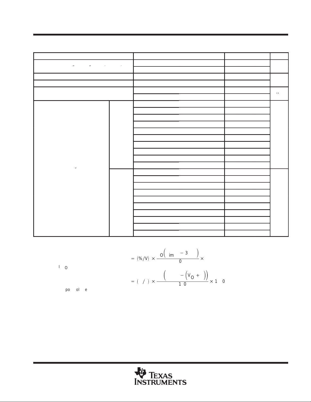
electrical characteristics over recommended operating free–air temperature range, V
I
= V
O(typ)
+
1 V, I
O
= 1 mA, EN = IN, C
O
= 4.7 µF (unless otherwise noted)
PARAMETER TEST CONDITIONS MIN TYP MAX UNIT
I
O
=
1
mA
to
100
mA
,
T
J
=
25°C
2
.
45
2
.
5
2
.
55
I
O
= 1 mA to 100 mA 2.425 2.5 2.575
TPS76425
I
O
= 1 mA to 150 mA, T
J
= 25°C 2.438 2.5 2.562
V
I
O
= 1 mA to 150 mA 2.407 2.5 2.593
I
O
= 1 mA to 100 mA, T
J
= 25°C 2.646 2.7 2.754
I
O
= 1 mA to 100 mA 2.619 2.7 2.781
TPS76427
I
O
= 1 mA to 150 mA, T
J
= 25°C 2.632 2.7 2.768
V
I
O
= 1 mA to 150 mA 2.598 2.7 2.8013
I
O
= 1 mA to 100 mA T
J
= 25°C 2.744 2.8 2.856
p
I
O
= 1 mA to 150 mA, 2.73 2.8 2.870
V
O
Out ut
voltage
TPS76428
I
O
= 1 mA to 150 mA, T
J
= 25°C 2.716 2.8 2.884
V
I
O
= 1 mA to 150 mA 2.695 2.8 2.905
I
O
= 1 mA to 100 mA, T
J
= 25°C 2.94 3.0 3.06
I
O
= 1 mA to 100 mA 2.925 3.0 3.075
TPS76430
I
O
= 1 mA to 150 mA, T
J
= 25°C 2.91 3.0 3.090
V
I
O
= 1 mA to 150 mA 2.887 3.0 3.112
I
O
= 1 mA to 100 mA, T
J
= 25°C 3.234 3.3 3.366
I
O
= 1 mA to 100 mA 3.201 3.3 3.399
TPS76433
I
O
= 1 mA to 150 mA, T
J
= 25°C 3.218 3.3 3.382
V
I
O
= 1 mA to 150 mA 3.177 3.3 3.423
I
Quiescent current
I
O
= 0 to 150 mA,
See Note 2
T
J
= 25°C,
85 100
(Q)
(GND
terminal
current)
I
O
= 0 to 150 mA, See Note 2 140
µ
A
EN < 0.5 V, T
J
= 25°C 0.5 1
µ
Standb
y
c
u
rrent
EN < 0.5 V 2
V
n
Output noise voltage
BW = 300 Hz to 50 kHz,
T
J
= 25°C,
C
o
= 10 µF,
See Note 2
50 µV
Bypass voltage T
J
= 25°C 1.192 V
PSRR Ripple rejection f = 1 kHz, C
o
= 10 µF, T
J
= 25°C, See Note 2 60 dB
Current limit T
J
= 25°C See Note 3 0.8 1.5 A
NOTES: 2. Minimum IN operating voltage is 2.7 V or V
O(typ)
+ 1 V, whichever is greater.
3. Test condition includes, output voltage V
O
=0 V and pulse duration = 10 mS.
TPS76425, TPS76427, TPS76428, TPS76430, TPS76433
LOW-POWER LOW-NOISE 150-mA LOW-DROPOUT LINEAR REGULATORS
SLVS180A – MARCH 1999 – REVISED JUNE 1999
5
POST OFFICE BOX 655303 • DALLAS, TEXAS 75265
electrical characteristics over recommended operating free–air temperature range,
V
I
= V
O(typ)
+ 1 V, I
O
= 1 mA, EN = IN, C
O
= 4.7 µF (unless otherwise noted) (continued)
PARAMETER TEST CONDITIONS MIN TYP MAX UNIT
Output voltage line regulation (∆V
/V
)
V
O
+ 1 V < V
I
≤ 10 V, V
I
≥ 3.5 V, T
J
= 25°C 0.04 0.07
gg(
OO
)
(see Note 4)
V
O
+ 1 V < V
I
≤ 10 V,
V
I
≥ 3.5 V 0.1
%/V
V
IH
EN high level input See Note 2 1.4 2
V
IL
EN low level input See Note 2 0.5 1.2
V
p
EN = 0 V –0.01 –0.5
I
I
EN
inp
u
t
c
u
rrent
EN = IN –0.01 –0.5
µ
A
I
O
= 0 mA, T
J
= 25°C 0.2
I
O
= 1 mA, T
J
= 25°C 3
I
O
= 50 mA, T
J
= 25°C 120 150
I
O
= 50 mA 200
I
O
= 75 mA, T
J
= 25°C 180 225
TPS76425
I
O
= 75 mA 300
mV
I
O
= 100 mA, T
J
= 25°C 240 300
I
O
= 100 mA 400
I
O
= 150 mA, T
J
= 25°C 360 450
Dropout voltage
I
O
= 150 mA 600
V
DO
g
(Note 5)
I
O
= 0 mA, T
J
= 25°C 0.2
I
O
= 1 mA, T
J
= 25°C 3
I
O
= 50 mA, T
J
= 25°C 100 125
I
O
= 50 mA 166
I
O
= 75 mA, T
J
= 25°C 150 188
TPS76433
I
O
= 75 mA 250
mV
I
O
= 100 mA, T
J
= 25°C 200 250
I
O
= 100 mA 333
I
O
= 150 mA, T
J
= 25°C 300 375
I
O
= 150 mA 500
NOTES: 2. Minimum IN operating voltage is 2.7 V or V
O(typ)
+ 1 V, whichever is greater.
4. If V
O
< 2.5 V and V
imax
= 10 V, V
imin
= 3.5 V:
Line Reg. (mV)
+
ǒ
%
ń
V
Ǔ
V
O
ǒ
V
imax
*
3.5 V
Ǔ
100
1000
If V
O
> 2.5 V and V
imax
= 10 V, V
imin
= V
O
+ 1 V:
Line Reg. (mV)
+
ǒ
%
ń
V
Ǔ
V
O
ǒ
V
imax
*
ǒ
V
O
)
1
Ǔ
Ǔ
100
1000
5. Dropout voltage is defined as the differential voltage between V
O
and V
i
when V
O
drops 100 mV below the value measured with
V
i
= V
O
+ 1.0 V .:
 Loading...