


 Loading...
Texas Instruments TPS76301DBV, TPS76316DBV, TPS76318DBV, TPS76325DBV, TPS76327DBV Schematic [ru]
...
|
TPS76301, TPS76316, TPS76318, TPS76325, TPS76327 |
|
TPS76328, TPS76330, TPS76333, TPS76338, TPS76350 |
www.ti.com |
LOW POWER 150 mA LOW DROPOUT LINEAR REGULATORS |
|
SLVS181H − DECEMBER 1998 − REVISED JANUARY 2004 |
D150-mA Low-Dropout Regulator
DOutput Voltage: 5 V, 3.8 V, 3.3 V, 3.0 V, 2.8 V, 2.7 V, 2.5 V, 1.8 V, 1.6 V and Variable
DDropout Voltage, Typically 300 mV at 150 mA
DThermal Protection
DOver Current Limitation
DLess Than 2- A Quiescent Current in
Shutdown Mode
D−40 °C to 125°C Operating Junction
Temperature Range
D5-Pin SOT-23 (DBV) Package
DBV PACKAGE (TOP VIEW)
IN |
|
1 |
5 |
|
OUT |
GND 2
EN |
|
3 |
4 |
|
NC/FB |
description
The TPS763xx family of low-dropout (LDO) voltage regulators offers the benefits of low-dropout voltage, low-power operation, and miniaturized packaging. These regulators feature low dropout voltages and quiescent currents compared to conventional LDO regulators. Offered in a 5-terminal, small outline integrated-circuit SOT-23 package, the TPS763xx series devices are ideal for cost-sensitive designs and for applications where board space is at a premium.
A combination of new circuit design and process innovation has enabled the usual pnp pass transistor to be replaced by a PMOS pass element. Because the PMOS pass element behaves as a low-value resistor, the dropout voltage is very low—typically 300 mV at 150 mA of load current (TPS76333)—and is directly proportional to the load current. Since the PMOS pass element is a voltage-driven device, the quiescent current is very low (140 A maximum) and is stable over the entire range of output load current (0 mA to 150 mA). Intended for use in portable systems such as laptops and cellular phones, the low-dropout voltage feature and low-power operation result in a significant increase in system battery operating life.
The TPS763xx also features a logic-enabled sleep mode to shut down the regulator, reducing quiescent current to 1 A maximum at TJ = 25°C.The TPS763xx is offered in 1.6-V,1.8-V, 2.5-V, 2.7-V, 2.8-V, 3.0-V, 3.3-V, 3.8-V, and 5-V fixed-voltage versions and in a variable version (programmable over the range of 1.5 V to 6.5 V.
AVAILABLE OPTIONS
TJ |
VOLTAGE |
PACKAGE |
PART NUMBER |
SYMBOL |
||
|
Variable |
|
TPS76301DBVT(1) |
TPS76301DBVR(2) |
PAZI |
|
|
1.6 V |
|
TPS76316DBVT |
TPS76316DBVR |
PBHI |
|
|
|
|
|
|
|
|
|
1.8 V |
|
TPS76318DBVT |
TPS76318DBVR |
PBAI |
|
|
|
|
|
|
|
|
|
2.5 V |
|
TPS76325DBVT |
TPS76325DBVR |
PBBI |
|
|
|
|
|
|
|
|
−40 °C to 125°C |
2.7 V |
SOT-23 |
TPS76327DBVT |
TPS76327DBVR |
PBCI |
|
|
|
|
|
|||
2.8 V |
(DBV) |
TPS76328DBVT |
TPS76328DBVR |
PBDI |
||
|
||||||
|
|
|
|
|
|
|
|
3.0 V |
|
TPS76330DBVT |
TPS76330DBVR |
PBII |
|
|
|
|
|
|
|
|
|
3.3 V |
|
TPS76333DBVT |
TPS76333DBVR |
PBEI |
|
|
|
|
|
|
|
|
|
3.8 V |
|
TPS76338DBVT |
TPS76338DBVR |
PBFI |
|
|
|
|
|
|
|
|
|
5.0 V |
|
TPS76350DBVT |
TPS76350DBVR |
PBGI |
|
(1)The DBVT passive indicates tape and reel of 250 parts.
(2)The DBVR passive indicates tape and reel of 3000 parts.
Please be aware that an important notice concerning availability, standard warranty, and use in critical applications of Texas Instruments semiconductor products and disclaimers thereto appears at the end of this data sheet.
All trademarks are the property of their respective owners.
PRODUCTION DATA information is current as of publication date. Products |
Copyright 2001 − 2004 Texas Instruments Incorporated |
conform to specifications per the terms of Texas Instruments standard warranty. |
|
Production processing does not necessarily include testing of all parameters. |
|
TPS76301, TPS76316, TPS76318, TPS76325, TPS76327 |
|
|
|
|
|
||||||||||||||||||||||||||||||||||||||
TPS76328, TPS76330, TPS76333, TPS76338, TPS76350 |
|
|
|
|
|
||||||||||||||||||||||||||||||||||||||
LOW POWER 150 mA LOW DROPOUT LINEAR REGULATORS |
|
|
|
|
www.ti.com |
||||||||||||||||||||||||||||||||||||||
SLVS181H − DECEMBER 1998 − REVISED JANUARY 2004 |
|
|
|
|
|
|
|
|
|
|
|
|
|
|
|
|
|
|
|
|
|
|
|
|
|
|
|
|
|
|
|
|
|
|
|||||||||
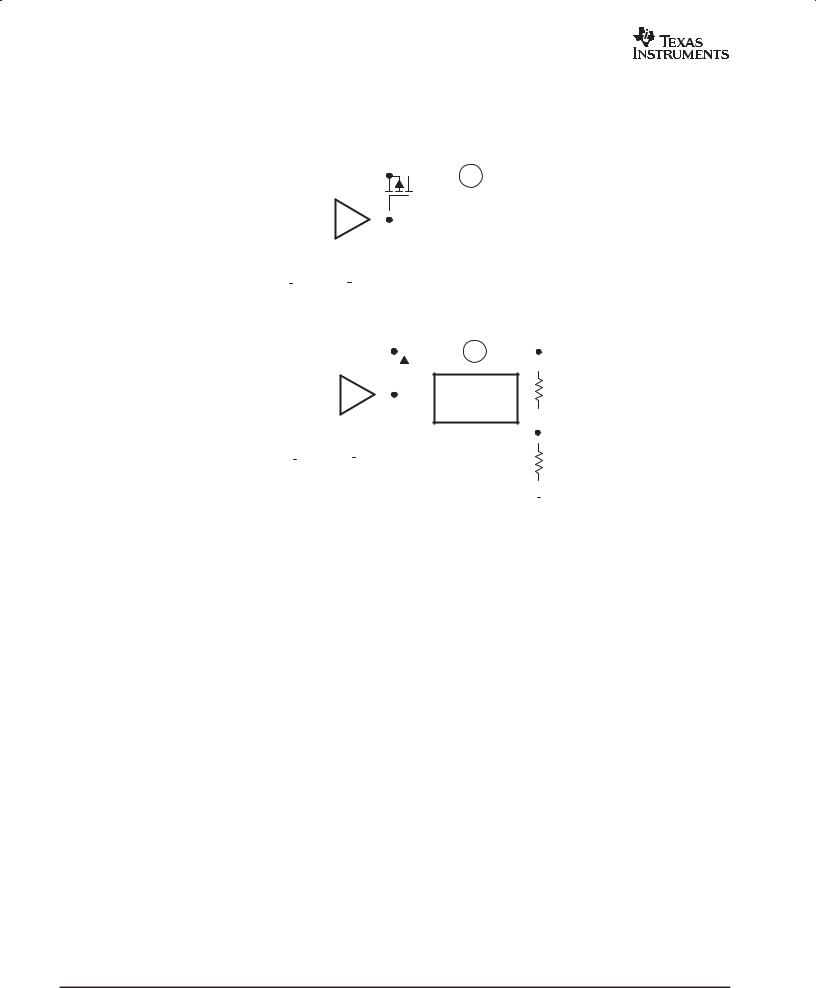
FUNCTIONAL BLOCK DIAGRAM |
|
|
|
|
|
|
|
|
|
|
|
|
|
|
|
|
|
|
|
|
|
|
|
|
|
|
|
|
|
|
|
|
|
|
|||||||||
|
|
|
|
|
|
|
|
|
|
|
|
|
|
|
|
|
|
|
|
|
TPS76301 |
|
|
|
|
|
|||||||||||||||||
IN |
|
|
|
|
|
|
|
|
|
|
|
|
|
|
|
|
|
|
|
|
|
|
|
|
|
|
|
|
|
|
|
|
|
|
|
|
|
OUT |
|||||
|
|
|
|
|
|
|
|
|
|
|
|
|
|
|
|
|
|
|
|
|
|
|
|
|
|
|
|
|
|
|
|
|
|
|
|
|
|
|
|||||
|
|
|
|
|
|
|
|
|
|
|
|
|
|
|
|
|
|
|
|
|
|
|
|
|
|
|
|
|
|
|
|
|
|
|
|
||||||||
EN |
|
|
|
|
|
|
|
|
|
|
|
|
|
|
|
|
|
|
|
|
|
|
|
|
|
|
|
|
|
|
|
|
|
|
|
|
|
|
|
|
|
|
|
|
|
|
|
|
|
|
|
|
|
|
|
|
|
|
|
|
|
|
|
|
|
|
|
|
|
|
|
|
|
|
|
|
|
|
|
|
|
|
|
|
|
|
|
|
|
|
|
|
|
|
|
|
|
|
|
|
|
|
|
|
|
|
|
|
|
|
|
|
|
|
|
|
|
|
|
|
Current Limit/ |
|
|
|
|
|
|
|
|
||
|
|
|
|
|
|
|
|
|
|
|
|
|
|
|
|
|
|
|
|
|
|
|
|
|
|
|
|
|
|
|
|
|
Thermal |
|
|
|
|
|
|
|
|
||
|
|
|
|
|
|
|
|
|
|
|
|
|
|
|
|
|
|
|
|
|
|
|
|
|
|
|
|
|
|
|
|
|
|
|
|
|
|
|
|
|
|||
|
|
VREF |
|
|
|
|
|
|
|
|
|
|
|
|
|
|
|
|
|
|
|
|
|
|
|
|
Protection |
|
|
|
|
FB |
|||||||||||
|
|
|
|
|
|
|
|
|
|
|
|
|
|
|
|
|
|
|
|
|
|
|
|
|
|
|
|
|
|
|
|
|
|
|
|
|
|
|
|
||||
GND |
|
|
|
|
|
|
|
|
|
|
|
|
|
|
|
|
|
|
|
|
|
|
|
|
|
|
|
|
|
|
|
|
|
|
|
|
|
|
|
||||
|
|
|
|
|
|
|
|
|
|
|
|
|
|
|
|
|
|
|
|
|
|
|
|
|
|
|
|
|
|
|
|
|
|
|
|
|
|
||||||
|
|
|
|
|
|
|
|
|
|
|
|
|
|
|
|
|
|
|
|
|
|
|
|
|
|
|
|
|
|
|
|
|
|
|
|
|
|
|
|
|
|||
|
|
|
|
|
|
|
|
|
|
|
|
|
|
|
|
|
|
|
|
|
|
|
|
|
|
|
|
|
|
|
|
|
|
|
|
|
|
|
|
|
|
|
|
|
|
|
|
|
|
|
|
|
|
TPS76316/ 18/ 25/ 27/ 28/ 30/ 33/ 38/ 50 |
|
|
|
|
|
||||||||||||||||||||||||||||
IN |
|
|
|
|
|
|
|
|
|
|
|
|
|
|
|
|
|
|
|
|
|
|
|
|
|
|
|
|
|
|
|
|
|
|
OUT |
||||||||
|
|
|
|
|
|
|
|
|
|
|
|
|
|
|
|
|
|
|
|
|
|
|
|
|
|
|
|
|
|
|
|
|
|
|
|
|
|
|
|
|
|||
|
|
|
|
|
|
|
|
|
|
|
|
|
|
|
|
|
|
|
|
|
|
|
|
|
|
|
|
|
|
|
|
|
|
|
|
|
|
|
|
|
|||
EN |
|
|
|
|
|
|
|
|
|
|
|
|
|
|
|
|
|
|
|
|
|
|
|
|
|
|
|
|
|
|
|
|
|
|
|
||||||||
|
|
|
|
|
|
|
|
|
|
|
|
|
|
|
|
|
|
|
|
|
|
|
|
|
|
|
|
|
|
|
|
|
|
|
|
|
|
|
|
|
|
||
|
|
|
|
|
|
|
|
|
|
|
|
|
|
|
|
|
|
|
|
|
|
|
|
|
|
|
|
|
|
|
|
|
Current Limit/ |
|
|
|
|
|
|||||
|
|
|
|
|
|
|
|
|
|
|
|
|
|
|
|
|
|
|
|
|
|
|
|
|
|
|
|
|
|
|
|
|
|
|
|
|
|
||||||
|
|
|
|
|
|
|
|
|
|
|
|
|
|
|
|
|
|
|
|
|
|
|
|
|
|
|
|
|
|
|
|
|
|
|
|
|
|
||||||
|
|
|
|
|
|
|
|
|
|
|
|
|
|
|
|
|
|
|
|
|
|
|
|
|
|
|
|
|
|
|
|
|
Thermal |
|
|
|
|
|
|||||
|
|
|
|
|
|
|
|
|
|
|
|
|
|
|
|
|
|
|
|
|
|
|
|
|
|
|
|
|
|
|
|
|
|
|
|
|
|
||||||
|
|
VREF |
|
|
|
|
|
|
|
|
|
|
|
|
|
|
|
|
|
|
|
|
|
|
|
|
Protection |
|
|
|
|
|
|||||||||||
GND |
|
|
|
|
|
|
|
|
|
|
|
|
|
|
|
|
|
|
|
|
|
|
|
|
|
|
|
|
|
|
|
|
|
|
|
|
|
|
|||||
|
|
|
|
|
|
|
|
|
|
|
|
|
|
|
|
|
|
|
|
|
|
|
|
|
|
|
|
|
|
|
|
|
|
||||||||||
|
|
|
|
|
|
|
|
|
|
|
|
|
|
|
|
|
|
|
|
|
|
|
|
|
|
|
|
|
|
|
|
|
|
|
|
|
|
||||||
|
|
|
|
|
|
|
|
|
|
|
|
|
|
|
|
|
|
|
|
|
|
|
|
|
|
|
|
|
|
|
|
|
|
|
|
|
|
|
|
|
|
|
|
|
|
|
|
|
|
|
|
|
|
|
|
|
|
|
|
|
|
|
|
|
|
|
|
|
|
|
|
|
|
|
|
|
|
|
|
|
|
|
|
|
|
|
|
|
|
|
|
|
|
|
|
|
|
|
|
|
|
|
|
|
|
|
|
|
|
|
|
|
|
|
|
|
|
|
|
|
|
|
|
|
|
|
|
|
|
|
|
|
|
|
|
|
|
|
|
|
|
|
|
|
|
|
|
|
|
|
|
|
|
|
|
|
|
|
|
|
|
|
|
|
|
|
|
|
|
|
|
|
|
|
|
TERMINAL |
|
NAME |
|
|
|
GND |
Ground |
|
|
EN |
Enable input |
|
|
FB |
Feedback voltage (TPS76301 only) |
|
|
IN |
Input supply voltage |
|
|
NC |
No connection (fixed-voltage option only) |
OUT |
Regulated output voltage |
|
Terminal Functions |
|
DESCRIPTION |
|
|
2

|
TPS76301, TPS76316, TPS76318, TPS76325, TPS76327 |
|
TPS76328, TPS76330, TPS76333, TPS76338, TPS76350 |
www.ti.com |
LOW POWER 150 mA LOW DROPOUT LINEAR REGULATORS |
|
SLVS181H − DECEMBER 1998 − REVISED JANUARY 2004 |
absolute maximum ratings over operating free-air temperature range (unless otherwise noted)1
Input voltage range(2) . . . . . . . . . . . . . . . . . . . . . . . . . . . . . . . . . . . . . . . . . . . . . . . . . |
. . . . . . . . . . . . . −0.3 V to 10 V |
|
Voltage range at EN . . . . . . . . . . . . . . . . . . . . . . . . . . . . . . . . . . . . . . . . . . . . . . . . . . |
. . . . . . . . . −0.3 V to V I + 0.3 |
V |
Voltage on OUT, FB . . . . . . . . . . . . . . . . . . . . . . . . . . . . . . . . . . . . . . . . . . . . . . . . . . . |
. . . . . . . . . . . . . . . . . . . . . . . 7 |
V |
Peak output current . . . . . . . . . . . . . . . . . . . . . . . . . . . . . . . . . . . . . . . . . . . . . . . . . . |
. . . . . . . . . . . Internally limited |
|
ESD rating, HBM . . . . . . . . . . . . . . . . . . . . . . . . . . . . . . . . . . . . . . . . . . . . . . . . . . . . |
. . . . . . . . . . . . . . . . . . . . . . 2 kV |
|
Continuous total power dissipation . . . . . . . . . . . . . . . . . . . . . . . . . . . . . . . . . . . . |
See Dissipation Rating Tables |
|
Operating junction temperature range, TJ . . . . . . . . . . . . . . . . . . . . . . . . . . . . . . . |
. . . . . . . . . . . . −40 °C to 150°C |
|
Storage temperature range, Tstg . . . . . . . . . . . . . . . . . . . . . . . . . . . . . . . . . . . . . . . |
. . . . . . . . . . . . −65 °C to 150°C |
|
(1)Stresses beyond those listed under absolute maximum ratings may cause permanent damage to the device. These are stress ratings only, and functional operation of the device at these or any other conditions beyond those indicated under recommended operating conditions is not implied. Exposure to absolute-maximum-rated conditions for extended periods may affect device reliability.
(2)All voltage values are with respect to network ground terminal.
DISSIPATION RATING TABLE
BOARD |
PACKAGE |
RθJC |
RθJA |
DERATING FACTOR |
TA ≤ 25°C |
TA = 70°C |
TA = 85°C |
|
ABOVE TA = 25°C |
POWER RATING |
POWER RATING |
POWER RATING |
|||||
|
|
|
|
|||||
Low K(1) |
DBV |
65.8 °C/W |
259 °C/W |
3.9 mW/°C |
386 mW |
212 mW |
154 mW |
|
High K(2) |
DBV |
65.8 °C/W |
180 °C/W |
5.6 mW/°C |
555 mW |
305 mW |
222 mW |
(1)The JEDEC Low K (1s) board design used to derive this data was a 3 inch x 3 inch, two layer board with 2 ounce copper traces on top of the board.
(2)The JEDEC High K (2s2p) board design used to derive this data was a 3 inch x 3 inch, multilayer board with 1 ounce internal power and ground planes and 2 ounce copper traces on top and bottom of the board.
recommended operating conditions
|
MIN NOM |
MAX |
UNIT |
|
|
|
|
Input voltage, V (1) |
2.7 |
10 |
V |
I |
|
|
|
Continuous output current, IO |
0 |
150 |
mA |
Operating junction temperature, TJ |
−40 |
125 |
°C |
(1) To calculate the minimum input voltage for your maximum output current, use the following equation: VI(min) = VO(max) + VDO(max load)
3

TPS76301, TPS76316, TPS76318, TPS76325, TPS76327 |
|
TPS76328, TPS76330, TPS76333, TPS76338, TPS76350 |
|
LOW POWER 150 mA LOW DROPOUT LINEAR REGULATORS |
www.ti.com |
SLVS181H − DECEMBER 1998 − REVISED JANUARY 2004 |
|
electrical characteristics over recommended operating free-air temperature range, VI = VO(typ) + 1 V, IO = 1 mA, EN = IN, Co = 4.7 F (unless otherwise noted)
|
PARAMETER |
|
TEST CONDITIONS |
MIN |
TYP |
MAX |
UNIT |
||
|
|
|
|
|
|
|
|
|
|
|
|
|
3.25 V > VI |
≥ 2.7 V, |
IO = 1 mA to 75 mA, |
0.98VO |
VO |
1.02VO |
|
|
|
|
2.5 V ≥ VO |
≥ 1.5 V, |
TJ = 25°C |
|
|||
|
|
|
3.25 V > VI ≥ 2.7 V, |
IO = 1 mA to 75 mA, |
0.97VO |
VO |
1.03VO |
|
|
|
|
|
2.5 V ≥ VO ≥ 1.5 V |
|
|
||||
|
|
|
|
|
|
|
|
||
|
|
|
VI ≥ 3.25 V, |
|
IO = 1 mA to 100 mA, |
0.98VO |
VO |
1.02VO |
|
|
|
|
5 V ≥ VO ≥ 1.5 V |
TJ = 25°C |
|
||||
|
|
TPS76301 |
|
|
|
V |
|||
|
|
VI ≥ 3.25 V, |
|
IO = 1 mA to 100 mA, |
0.97VO |
VO |
1.03VO |
||
|
|
|
|
|
|||||
|
|
|
5 V ≥ VO ≥ 1.5 V |
|
|
||||
|
|
|
VI ≥ 3.25 V, |
|
IO = 1 mA to 150 mA, |
0.975VO |
VO |
1.025VO |
|
|
|
|
5 V ≥ VO ≥ 1.5 V |
TJ = 25°C |
|
||||
|
|
|
|
|
|
|
|||
|
|
|
VI ≥ 3.25 V, |
|
IO = 1 mA to 150 mA, |
0.9625VO |
VO |
1.0375VO |
|
|
|
|
5 V ≥ VO ≥ 1.5 V |
|
|
||||
|
|
|
|
|
|
|
|
||
|
|
|
VI = 2.7 V, |
|
1 mA< IO < 75 mA, |
1.568 |
1.6 |
1.632 |
|
|
|
|
|
TJ = 25°C |
|
||||
|
|
|
|
|
|
|
|
|
|
|
|
|
VI = 2.7 V, |
|
1 mA< IO < 75 mA |
1.552 |
1.6 |
1.648 |
|
|
|
|
VI = 3.25 V, |
|
1 mA < IO < 100 mA, |
1.568 |
1.6 |
1.632 |
|
|
|
TPS76316 |
|
TJ = 25°C |
V |
||||
|
|
|
|
|
|
|
|||
|
|
|
VI = 3.25 V, |
|
1 mA < IO < 100 mA |
1.552 |
1.6 |
1.648 |
|
|
|
|
VI = 3.25 V, |
|
1 mA < IO < 150 mA, |
1.560 |
1.6 |
1.640 |
|
|
|
|
|
TJ = 25°C |
|
||||
|
|
|
|
|
|
|
|
|
|
|
|
|
VI = 3.25 V, |
|
1 mA < IO < 150 mA |
1.536 |
1.6 |
1.664 |
|
|
|
|
VI = 2.7 V, |
|
1 mA< IO < 75 mA, |
1.764 |
1.8 |
1.836 |
|
|
|
|
|
TJ = 25°C |
|
||||
VO |
Output voltage |
|
VI = 2.7 V, |
|
1 mA< IO < 75 mA |
1.746 |
1.8 |
1.854 |
|
|
VI = 3.25 V, |
|
1 mA < IO < 100 mA, |
1.764 |
1.8 |
1.836 |
|
||
|
|
TPS76318 |
|
TJ = 25°C |
V |
||||
|
|
|
|
|
|
|
|||
|
|
|
VI = 3.25 V, |
|
1 mA < IO < 100 mA |
1.746 |
1.8 |
1.854 |
|
|
|
|
VI = 3.25 V, |
|
1 mA < IO < 150 mA, |
1.755 |
1.8 |
1.845 |
|
|
|
|
|
TJ = 25°C |
|
||||
|
|
|
|
|
|
|
|
|
|
|
|
|
VI = 3.25 V, |
|
1 mA < IO < 150 mA |
1.733 |
1.8 |
1.867 |
|
|
|
|
IO = 1 mA to 100 mA, |
TJ = 25°C |
2.45 |
2.5 |
2.55 |
|
|
|
|
TPS76325 |
IO = 1 mA to 100 mA |
|
2.425 |
2.5 |
2.575 |
V |
|
|
|
IO = 1 mA to 150 mA, |
TJ = 25°C |
2.438 |
2.5 |
2.562 |
|||
|
|
|
|
||||||
|
|
|
IO = 1 mA to 150 mA |
|
2.407 |
2.5 |
2.593 |
|
|
|
|
|
IO = 1 mA to 100 mA, |
TJ = 25°C |
2.646 |
2.7 |
2.754 |
|
|
|
|
TPS76327 |
IO = 1 mA to 100 mA |
|
2.619 |
2.7 |
2.781 |
V |
|
|
|
IO = 1 mA to 150 mA, |
TJ = 25°C |
2.632 |
2.7 |
2.767 |
|||
|
|
|
|
||||||
|
|
|
IO = 1 mA to 150 mA |
|
2.599 |
2.7 |
2.801 |
|
|
|
|
|
IO = 1 mA to 100 mA, |
TJ = 25°C |
2.744 |
2.8 |
2.856 |
|
|
|
|
TPS76328 |
IO = 1 mA to 100 mA |
|
2.716 |
2.8 |
2.884 |
V |
|
|
|
IO = 1 mA to 150 mA, |
TJ = 25°C |
2.73 |
2.8 |
2.87 |
|||
|
|
|
|
||||||
|
|
|
IO = 1 mA to 150 mA |
|
2.695 |
2.8 |
2.905 |
|
|
|
|
|
IO = 1 mA to 100 mA, |
TJ = 25°C |
2.94 |
3.0 |
3.06 |
|
|
|
|
TPS76330 |
IO = 1 mA to 100 mA |
|
2.91 |
3.0 |
3.09 |
V |
|
|
|
IO = 1 mA to 150 mA, |
TJ = 25°C |
2.925 |
3.0 |
3.075 |
|||
|
|
|
|
||||||
|
|
|
IO = 1 mA to 150 mA |
|
2.888 |
3.0 |
3.112 |
|
|
4

|
TPS76301, TPS76316, TPS76318, TPS76325, TPS76327 |
|
TPS76328, TPS76330, TPS76333, TPS76338, TPS76350 |
www.ti.com |
LOW POWER 150 mA LOW DROPOUT LINEAR REGULATORS |
|
SLVS181H − DECEMBER 1998 − REVISED JANUARY 2004 |
electrical characteristics over recommended operating free-air temperature range,
VI = VO(typ) + 1 V, IO = 1 mA, EN = IN, Co = 4.7 F (unless otherwise noted) (continued)
|
PARAMETER |
|
|
TEST CONDITIONS |
MIN |
TYP |
MAX |
UNIT |
||
|
|
|
|
|
|
|
|
|
|
|
|
|
|
IO = 1 mA to 100 mA, |
TJ = 25°C |
3.234 |
3.3 |
3.366 |
|
||
|
|
TPS76333 |
IO = 1 mA to 100 mA |
|
3.201 |
3.3 |
3.399 |
V |
||
|
|
IO = 1 mA to 150 mA, |
TJ = 25°C |
3.218 |
3.3 |
3.382 |
||||
|
|
|
|
|||||||
|
|
|
IO = 1 mA to 150 mA |
|
3.177 |
3.3 |
3.423 |
|
||
|
|
|
IO = 1 mA to 100 mA, |
TJ = 25°C |
3.724 |
3.8 |
3.876 |
|
||
VO |
Output voltage |
TPS76338 |
IO = 1 mA to 100 mA |
|
3.705 |
3.8 |
3.895 |
V |
||
IO = 1 mA to 150 mA, |
TJ = 25°C |
3.686 |
3.8 |
3.914 |
||||||
|
|
|
|
|||||||
|
|
|
IO = 1 mA to 150 mA |
|
3.667 |
3.8 |
3.933 |
|
||
|
|
|
IO = 1 mA to 100 mA, |
TJ = 25°C |
4.875 |
5 |
5.125 |
|
||
|
|
TPS76350 |
IO = 1 mA to 100 mA |
|
4.825 |
5 |
5.175 |
V |
||
|
|
IO = 1 mA to 150 mA, |
TJ = 25°C |
4.750 |
5 |
5.15 |
||||
|
|
|
|
|||||||
|
|
|
IO = 1 mA to 150 mA |
|
4.80 |
5 |
5.20 |
|
||
I(Q) |
Quiescent current |
|
IO = 0 to 150 mA, |
TJ = 25°C (1) |
|
85 |
100 |
|
||
(GND terminal current) |
IO = 0 to 150 mA |
(2) |
|
|
140 |
A |
||||
|
|
|
||||||||
|
Standby current |
|
EN < 0.5 V, |
TJ = 25°C |
|
0.5 |
1 |
|||
|
|
|
|
|||||||
|
|
EN < 0.5 V |
|
|
|
2 |
|
|||
|
|
|
|
|
|
|
||||
|
|
|
|
|
|
|
|
|
||
Vn |
Output noise voltage |
|
BW = 300 Hz to 50 kHz, |
Co = 10 F (2) |
|
140 |
|
V |
||
|
TJ = 25°C, |
|
|
|||||||
PSRR |
Ripple rejection |
|
f = 1 kHz, Co = 10 F, |
TJ = 25°C (2) |
|
60 |
|
dB |
||
|
Current limit |
|
TJ = 25°C |
(3) |
0.5 |
0.8 |
1.5 |
A |
||
|
Output voltage line regulation |
VO + 1 V < VI ≤ 10 V, |
VI ≥ 3.5 V, TJ = 25°C |
|
0.04 |
0.07 |
%/V |
|||
|
(∆VO/VO) (see Note 3) |
V |
+ 1 V < V ≤ 10 V, |
V ≥ 3.5 V |
|
|
0.1 |
|||
|
|
|
|
|||||||
|
|
|
O |
I |
I |
|
|
|
|
|
VIH |
EN high level input |
|
(2) |
|
|
|
1.4 |
2 |
V |
|
VIL |
EN low level input |
|
(2) |
|
|
0.5 |
1.2 |
|
||
|
|
|
|
|
||||||
II |
EN input current |
|
EN = 0 V |
|
|
−0.01 |
−0.5 |
A |
||
|
|
|
|
|
|
|
||||
|
EN = IN |
|
|
−0.01 |
−0.5 |
|||||
|
|
|
|
|
|
|||||
(1)Minimum IN operating voltage is 2.7 V or VO(typ) + 1 V, whichever is greater.
(2)Test condition includes, output voltage VO=0 volts (for variable device FB is shorted to VO), and pulse duration = 10 mS.
(3)If VO < 2.5 V and VImax = 10 V, VImin = 3.5 V:
VO VImax |
* 3.5 V |
|
|
|
||
Line Reg. (mV) + % V |
|
|
|
1000 |
|
|
|
|
|
|
|||
100 |
|
|
|
|
||
If VO > 2.5 V and VImax = 10 V, VImin = VO + 1 V: |
|
|
|
|
|
|
VO VImax * VO ) 1 |
|
|||||
Line Reg. (mV) + % V |
|
|
|
|
|
1000 |
|
100 |
|
|
|
||
|
|
|
|
|
|
|
5

TPS76301, TPS76316, TPS76318, TPS76325, TPS76327 |
|
TPS76328, TPS76330, TPS76333, TPS76338, TPS76350 |
|
LOW POWER 150 mA LOW DROPOUT LINEAR REGULATORS |
www.ti.com |
SLVS181H − DECEMBER 1998 − REVISED JANUARY 2004 |
|
electrical characteristics over recommended operating free-air temperature range,
VI = VO(typ) + 1 V, IO = 1 mA, EN = IN, Co = 4.7 F (unless otherwise noted) (continued)
PARAMETER |
|
|
TEST CONDITIONS |
MIN TYP |
MAX |
UNIT |
|
|
|
|
|
|
|
|
|
|
|
IO = 0 mA, |
|
TJ = 25°C |
0.2 |
|
|
|
|
IO = 1 mA, |
|
TJ = 25°C |
3 |
|
|
|
|
IO = 50 mA, |
|
TJ = 25°C |
120 |
150 |
|
|
|
IO = 50 mA |
|
|
|
200 |
|
|
TPS76325 |
IO = 75 mA, |
|
TJ = 25°C |
180 |
225 |
mV |
|
IO = 75 mA |
|
|
|
300 |
||
|
|
|
|
|
|
||
|
|
IO = 100 mA, |
|
TJ = 25°C |
240 |
300 |
|
|
|
IO = 100 mA |
|
|
|
400 |
|
|
|
IO = 150 mA, |
|
TJ = 25°C |
360 |
450 |
|
|
|
IO = 150 mA |
|
|
|
600 |
|
|
|
IO = 0 mA, |
|
TJ = 25°C |
0.2 |
|
|
|
|
IO = 1 mA, |
|
TJ = 25°C |
3 |
|
|
|
|
IO = 50 mA, |
|
TJ = 25°C |
100 |
125 |
|
|
|
IO = 50 mA |
|
|
|
166 |
|
VDO Dropout voltage |
TPS76333 |
IO = 75 mA, |
|
TJ = 25°C |
150 |
188 |
mV |
IO = 75 mA |
|
|
|
250 |
|||
|
|
|
|
|
|
||
|
|
IO = 100 mA, |
|
TJ = 25°C |
200 |
250 |
|
|
|
IO = 100 mA |
|
|
|
333 |
|
|
|
IO = 150 mA, |
|
TJ = 25°C |
300 |
375 |
|
|
|
IO = 150 mA |
|
|
|
500 |
|
|
|
IO = 0 mA, |
|
TJ = 25°C |
0.2 |
|
|
|
|
IO = 1 mA, |
|
TJ = 25°C |
2 |
|
|
|
|
IO = 50 mA, |
|
TJ = 25°C |
60 |
75 |
|
|
|
IO = 50 mA |
|
|
|
100 |
|
|
TPS76350 |
IO = 75 mA, |
|
TJ = 25°C |
90 |
113 |
mV |
|
IO = 75 mA |
|
|
|
150 |
||
|
|
|
|
|
|
||
|
|
IO = 100 mA, |
|
TJ = 25°C |
120 |
150 |
|
|
|
IO = 100 mA |
|
|
|
200 |
|
|
|
IO = 150 mA, |
|
TJ = 25°C |
180 |
225 |
|
|
|
IO = 150 mA |
|
|
|
300 |
|
6

|
TPS76301, TPS76316, TPS76318, TPS76325, TPS76327 |
|
TPS76328, TPS76330, TPS76333, TPS76338, TPS76350 |
www.ti.com |
LOW POWER 150 mA LOW DROPOUT LINEAR REGULATORS |
|
SLVS181H − DECEMBER 1998 − REVISED JANUARY 2004 |
|
TYPICAL CHARACTERISTICS |
VO− Output Voltage − V
VO− Output Voltage − V
2.505
2.5
2.495
2.49
2.485
2.48
2.475
0
5.01
5
4.99
4.98
4.97
4.96
4.95
0
TPS76325
OUTPUT VOLTAGE vs
OUTPUT CURRENT
|
|
|
|
|
|
|
|
|
|
|
|
1.805 |
|
|
|
|
|
|
|
|
VI = 3.5 V |
|
|
|
|
|
|||
|
|
|
|
|
|
|
|
|
|
|
|
|||
|
|
|
|
|
|
CI = CO = 4.7 F |
|
|
|
|
||||
|
|
|
|
|
|
TJ = 25°C |
|
|
1.800 |
|
||||
|
|
|
|
|
|
|
|
|||||||
|
|
|
|
|
|
|
|
|
|
|
− V |
1.795 |
|
|
|
|
|
|
|
|
|
|
|
|
|
|
|
||
|
|
|
|
|
|
|
|
|
|
|
Voltage |
1.790 |
|
|
|
|
|
|
|
|
|
|
|
|
|
Output− |
1.785 |
|
|
|
|
|
|
|
|
|
|
|
|
|
|
|
||
|
|
|
|
|
|
|
|
|
|
|
O |
1.780 |
|
|
|
|
|
|
|
|
|
|
|
|
|
V |
|
|
|
|
|
|
|
|
|
|
|
|
|
|
|
1.775 |
|
|
|
|
|
|
|
|
|
|
|
|
|
|
1.770 |
|
|
30 |
60 |
90 |
120 |
150 |
180 |
|||||||||
|
||||||||||||||
0 |
||||||||||||||
|
|
|
|
|
|
|
|
|
|
|
|
|||
IO − Output Current − mA
TPS76318
OUTPUT VOLTAGE vs
OUTPUT CURRENT
VI = 3.5 V
CI = CO = 4.7 F
TJ = 25°C
30 |
60 |
90 |
120 |
150 |
180 |
IO − Output Current − mA
Figure 1 |
Figure 2 |
|
TPS76350 |
TPS76325 |
|
OUTPUT VOLTAGE |
||
OUTPUT VOLTAGE |
||
vs |
||
vs |
||
OUTPUT CURRENT |
||
FREE-AIR TEMPERATURE |
||
|
|
|
|
VI = 6 V |
|
|
2.53 |
|
|
|
|
|
|
|
|
|
|
|
|
|
|
|
|
|
|
|
|
|
V = 3.5 V |
|
|
|||
|
|
|
CI = CO = 4.7 F |
|
|
|
|
|
|
|
I |
|
|
|
||
|
|
|
|
|
|
|
|
|
|
CI = CO = 4.7 F |
|
|||||
|
|
|
TJ = 25°C |
|
|
2.52 |
|
|
|
|
|
|
|
|
|
|
|
|
|
|
|
− V |
2.51 |
|
|
|
|
|
|
|
|
|
|
|
|
|
|
|
Voltage |
2.5 |
|
IO = 1 mA |
|
|
|
|
|
|
||
|
|
|
|
|
|
|
|
|
|
|
|
|
|
|||
|
|
|
|
|
− Output |
2.49 |
IO = 150 mA |
|
|
|
|
|
|
|||
|
|
|
|
|
O |
|
|
|
|
|
|
|
|
|
|
|
|
|
|
|
|
V |
|
|
|
|
|
|
|
|
|
|
|
|
|
|
|
|
|
2.48 |
|
|
|
|
|
|
|
|
|
|
30 |
60 |
90 |
120 |
150 |
180 |
2.47 |
|
|
|
|
|
|
|
|
|
|
−55 |
−35 |
−15 |
5 |
25 |
45 |
65 |
85 |
105 |
125 |
|||||||
|
IO − Output Current − mA |
|
|
|||||||||||||
|
|
|
|
|
TJ − Junction Temperature − |
°C |
|
|
||||||||
|
|
|
|
|
|
|
|
|
|
|||||||
Figure 3 |
Figure 4 |
7
Loading...