


TEXAS INSTRUMENTS TPS79401, TPS79418, TPS79425, TPS79428, TPS79430 Technical data
...TPS79401
TPS79401, TPS79418
TPS79425, TPS79428
TPS79430, TPS79433
www.ti.com |
SLVS349D –NOVEMBER 2001 –REVISED OCTOBER 2004 |
|
ULTRALOW-NOISE, HIGH PSRR, FAST RF 250-mA LOW-DROPOUT LINEAR REGULATORS
FEATURES
∙250-mA Low-Dropout Regulator With Enable
∙Available in 1.8 V, 2.5 V, 2.8 V, 3 V, 3.3 V, and Adjustable (1.2 V to 5.5 V)
∙High PSRR (60 dB at 10 kHz)
∙Ultralow Noise (32 µVrms, TPS79428)
∙Fast Start-Up Time (50 µs)
∙Stable With a 2.2-µF Ceramic Capacitor
∙Excellent Load/Line Transient Response
∙Very Low Dropout Voltage (155 mV at Full Load)
∙Available in MSOP-8 and SOT223-6 Packages
APPLICATIONS
∙RF: VCOs, Receivers, ADCs
∙Audio
∙ Bluetooth™, Wireless LAN
∙Cellular and Cordless Telephones
∙Handheld Organizers, PDAs
DESCRIPTION
The TPS794xx family of low-dropout (LDO) linear voltage regulators features high power-supply rejection ratio (PSRR), ultralow-noise, fast start-up, and excellent line and load transient responses in small outline, MSOP-8 PowerPAD™ and SOT223-6 packages. Each device in the family is stable with a small 2.2-µF ceramic capacitor on the output. The family uses an advanced, proprietary BiCMOS fabrication process to yield extremely low dropout voltages (e.g., 155 mV at 250 mA). Each device achieves fast start-up times (approximately 50 µs with a 0.001-µF bypass capacitor) while consuming low quiescent current (170 µA typical). Moreover, when the device is placed in standby mode, the supply current is reduced to less than 1 µA. The TPS79428 exhibits approximately 32 µVRMS of output voltage noise at 2.8 V output with a 0.1-µF bypass capacitor. Applications with analog components that are noise-sensitive, such as portable RF electronics, benefit from the high PSRR and low noise features as well as the fast response time.
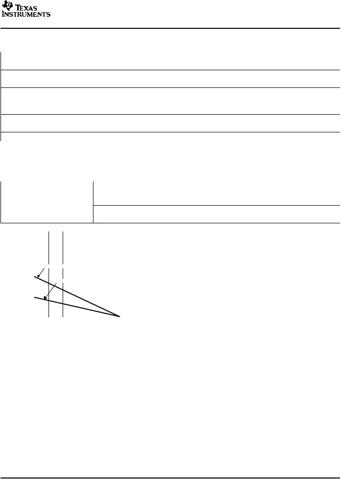
DGN PACKAGE
MSOP PowerPAD |
TPS79433 |
TPS79428 |
(TOP VIEW) |
RIPPLE REJECTION |
OUTPUT SPECTRAL NOISE DENSITY |
OUT |
1 |
8 |
IN |
|
|
|
vs |
|
|
|
|
|
|
FREQUENCY |
|
|
|
||||||
NC |
2 |
7 |
NC |
|
|
|
|
|
|||
90 |
|
|
|
|
|
|
0.35 |
||||
FB |
3 |
6 |
EN |
|
|
|
|
|
√Hz) |
||
|
|
|
|
|
|
|
|||||
NR |
4 |
5 |
GND |
80 |
|
IOUT = 10 mA |
|
0.30 |
|||
|
|
|
|
|
|
|
(μV/ |
||||
NC − No internal connection |
70 |
|
|
|
IOUT = 250 mA |
|
|||||
|
|
|
Rejection (dB) |
|
|
|
|
Noise Density |
0.25 |
||
|
|
|
60 |
|
|
|
|
|
|||
|
|
|
|
|
|
|
|
|
|||
|
DCQ PACKAGE |
50 |
|
|
|
|
|
0.20 |
|||
|
SOT223-6 |
|
|
|
|
|
|
||||
|
|
|
|
|
|
|
|
||||
|
(TOP VIEW) |
40 |
|
|
|
|
|
0.15 |
|||
|
Ripple |
|
|
|
|
|
Spectral |
||||
EN |
1 |
|
30 |
VIN = 4.3 V, |
|
|
|
0.10 |
|||
2 |
|
20 |
VOUT = 3.3 V, |
|
|
|
|||||
IN |
|
6 |
CIN = 1 μF, |
|
|
|
Output |
|
|||
GND |
3 |
|
|
|
|
|
0.05 |
||||
|
|
|
μ |
|
|
|
|||||
|
GND |
10 |
COUT = 10 F, |
|
|
|
|
||||
OUT |
4 |
|
|
|
CNR = 0.01 μF |
|
|
|
|
0 |
|
|
|
0 |
|
|
|
|
|
|
|||
|
|
|
|
|
|
|
|
|
|
|
|
NR |
5 |
|
|
10 |
100 |
1 k |
10 k |
100 k |
1 M |
10 M |
|
Frequency (Hz)
|
|
vs |
|
|
FREQUENCY |
|
|
|
|
COUT = 2.2 μF, |
|
|
|
CNR = 0.1 μF, |
|
|
|
VIN = 3.8 V |
|
|
IOUT = 250 mA |
|
|
|
|
IOUT = 1 mA |
|
100 |
1000 |
10000 |
100000 |
Frequency (Hz)
Please be aware that an important notice concerning availability, standard warranty, and use in critical applications of Texas Instruments semiconductor products and disclaimers thereto appears at the end of this data sheet.
Bluetooth is a trademark of Bluetooth SIG, Inc. PowerPAD is a trademark of Texas Instruments.
All other trademarks are the property of their respective owners.
PRODUCTION DATA information is current as of publication date. |
Copyright © 2001–2004, Texas Instruments Incorporated |
Products conform to specifications per the terms of the Texas |
|
Instruments standard warranty. Production processing does not |
|
necessarily include testing of all parameters. |
|

TPS79401, TPS79418 |
|
|
TPS79425, TPS79428 |
|
|
TPS79430, TPS79433 |
www.ti.com |
|
SLVS349D –NOVEMBER 2001 –REVISED OCTOBER 2004 |
||
|
This integrated circuit can be damaged by ESD. Texas Instruments recommends that all integrated circuits be handled with appropriate precautions. Failure to observe proper handling and installation procedures can cause damage.
ESD damage can range from subtle performance degradation to complete device failure. Precision integrated circuits may be more susceptible to damage because very small parametric changes could cause the device not to meet its published specifications.
ORDERING INFORMATION
PRODUCT |
VOLTAGE |
PACKAGE |
TJ |
SYMBOL |
PART NUMBER |
TRANSPORT MEDIA, |
QUANTITY |
||||||
|
|
MSOP-8 |
|
AXL |
TPS79401DGNR |
Tape and Reel, 2500 |
|
|
|
TPS79401DGNT |
Tape and Reel, 250 |
||
TPS79401 |
Adjustable |
|
|
|
||
|
|
|
TPS79401DCQR |
Tape and Reel, 2500 |
||
|
|
SOT223-6 |
|
PS79401 |
||
|
|
|
TPS79401DCQ |
Tube, 78 |
||
|
|
|
|
|
||
|
|
MSOP-8 |
|
AXM |
TPS79418DGNR |
Tape and Reel, 2500 |
|
|
|
TPS79418DGNT |
Tape and Reel, 250 |
||
TPS79418 |
1.8 V |
|
|
|
||
|
|
|
TPS79418DCQR |
Tape and Reel, 2500 |
||
|
|
SOT223-6 |
|
PS79418 |
||
|
|
|
TPS79418DCQ |
Tube, 78 |
||
|
|
|
|
|
||
|
|
MSOP-8 |
|
AYB |
TPS79425DGNR |
Tape and Reel, 2500 |
|
|
|
TPS79425DGNT |
Tape and Reel, 250 |
||
TPS79423 |
2.5 V |
|
|
|
||
|
|
|
TPS79425DCQR |
Tape and Reel, 2500 |
||
|
|
SOT223-6 |
|
PS79425 |
||
|
|
|
TPS79425DCQ |
Tube, 78 |
||
|
|
|
-40°C to 125°C |
|
||
|
|
|
|
TPS79428DGNR |
Tape and Reel, 2500 |
|
|
|
MSOP-8 |
|
AYC |
||
|
|
|
TPS79428DGNT |
Tape and Reel, 250 |
||
TPS79428 |
2.8 V |
|
|
|
||
|
|
|
TPS79428DCQR |
Tape and Reel, 2500 |
||
|
|
SOT223-6 |
|
PS79428 |
||
|
|
|
TPS79428DCQ |
Tube, 78 |
||
|
|
|
|
|
||
|
|
MSOP-8 |
|
AYD |
TPS79430DGNR |
Tape and Reel, 2500 |
|
|
|
TPS79430DGNT |
Tape and Reel, 250 |
||
TPS79430 |
3 V |
|
|
|
||
|
|
|
TPS79430DCQR |
Tape and Reel, 2500 |
||
|
|
SOT223-6 |
|
PS79430 |
||
|
|
|
TPS79430DCQ |
Tube, 78 |
||
|
|
|
|
|
||
|
|
MSOP-8 |
|
AYE |
TPS79433DGNR |
Tape and Reel, 2500 |
|
|
|
TPS79433DGNT |
Tape and Reel, 250 |
||
TPS79433 |
3.3 V |
|
|
|
||
|
|
|
TPS79433DCQR |
Tape and Reel, 2500 |
||
|
|
SOT223-6 |
|
PS79433 |
||
|
|
|
TPS79433DCQ |
Tube, 78 |
||
|
|
|
|
|
2
|
TPS79401, TPS79418 |
|
|
TPS79425, TPS79428 |
|
www.ti.com |
TPS79430, TPS79433 |
|
SLVS349D –NOVEMBER 2001 –REVISED OCTOBER 2004 |
||
|
||
ABSOLUTE MAXIMUM RATINGS |
|
|
over operating temperature range unless otherwise noted(1) |
|
|
|
VALUE |
|
VIN range |
-0.3 V to 6 V |
|
VEN range |
-0.3 V to VIN + 0.3 V |
|
VOUT range |
-0.3 V to 6 V |
|
Peak output current |
Internally limited |
|
ESD rating, HBM |
2 kV |
|
ESD rating, CDM |
500 V |
|
Continuous total power dissipation |
See Dissipation Ratings Table |
|
Junction temperature range, TJ |
-40°C to 150°C |
|
Storage temperature range, Tstg |
-65°C to 150°C |
(1)Stresses beyond those listed under absolute maximum ratings may cause permanent damage to the device. These are stress ratings only, and functional operation of the device at these or any other conditions beyond those indicated under recommended operating conditions is not implied. Exposure to absolute-maximum-rated conditions for extended periods may affect device reliability.
PACKAGE DISSIPATION RATINGS
PACKAGE |
AIR FLOW |
RθJC(°C/W) RθJA(°C/W) |
TA ≤ 25°C |
TA = 70°C |
TA = 85°C |
|
(CFM) |
POWER RATING |
POWER RATING |
POWER RATING |
|||
|
0 |
8.47 |
55.09 |
2.27 W |
1.45 W |
1.18 W |
DGN |
150 |
8.21 |
49.97 |
2.50 W |
1.60 W |
1.30 W |
|
250 |
8.20 |
48.10 |
2.60 W |
1.66 W |
1.35 W |
PD (W)
6 |
|
|
|
|
|
|
|
|
|
|
|
|
|
|
|
5 |
|
|
|
|
|
|
|
|
|
|
|
|
|
|
|
|
|
|
|
|
|
|
|
|
|
|
|
|
|
|
|
4 |
|
|
|
|
|
|
|
|
|
|
|
|
|
|
|
|
|
|
|
|
|
|
|
|
|
|
|
|
|
|
|
|
|
Condition 1 |
|
|
|
|
|
|
|
|
CONDITIONS |
PACKAGE |
PCB AREA |
θJA |
|
3 |
|
|
|
|
|
|
|
|
|
|
|
1 |
SOT223 |
4in2 Top Side Only |
53°C/W |
|
|
Condition 2 |
|
|
|
|
|
|
|
||||||
|
|
|
|
|
|
|
|
|
|
||||||
2 |
|
|
|
|
|
|
|
|
|
2 |
SOT223 |
0.5in2 Top Side Only |
110°C/W |
||
|
|
|
|
|
|
|
|
|
|
|
|||||
1 |
|
|
|
|
|
|
|
|
|
|
|
|
|
|
|
|
|
|
|
|
|
|
|
|
|
|
|
|
|
|
|
0 |
|
|
|
|
|
|
|
|
|
|
|
|
|
|
|
0 |
25 |
50 |
75 |
100 |
125 |
150 |
|
|
|
|
|||||
|
|
|
|
TA (°C) |
|
|
|
|
|
|
|
|
|
|
|
Figure 1. SOT223 Power Dissipation
3
TPS79401, TPS79418 |
|
|
TPS79425, TPS79428 |
|
|
TPS79430, TPS79433 |
www.ti.com |
|
SLVS349D –NOVEMBER 2001 –REVISED OCTOBER 2004 |
||
|
ELECTRICAL CHARACTERISTICS
Over recommended operating temperature range (TJ = -40°C to 125°C), VEN = VIN, VIN = VOUT(nom) + 1 V(1), IOUT = 1mA, COUT = 10µF, CNR = 0.01 µF, unless otherwise noted. Typical values are at 25°C.
|
PARAMETER |
|
TEST CONDITIONS |
|
|
MIN |
TYP |
MAX |
UNIT |
V |
Input voltage(1) |
|
|
|
|
2.7 |
|
5.5 |
V |
IN |
|
|
|
|
|
|
|
|
|
IOUT |
Continuous output current |
|
|
|
|
0 |
|
250 |
mA |
VFB |
Internal reference |
TPS79401 TJ = 25°C |
|
|
1.220 |
1.225 |
1.230 |
V |
|
VOUT |
Output voltage range |
TPS79401 |
|
|
|
VFB |
|
5.5 - VDO |
V |
|
Accuracy(1) |
V |
+ 1 V ≤ V ≤ 5.5 V 0 mA ≤ I |
OUT |
≤ 250 mA |
-3.0 |
|
+3.0 |
% |
|
|
OUT |
IN |
|
|
|
|
|
|
Output voltage line regulation ( VOUT%/ VIN)(1)
Load regulation ( VOUT%/ IOUT) TPS79428
Dropout voltage(2)
TPS79430
VIN = VOUT(nom) - 0.1 V
TPS79433
Output current limit
Ground pin current
Shutdown current(3)
FB pin current
Power-supply ripple
TPS79428
rejection
Output noise voltage (TPS79428)
Time, start-up (TPS79428)
High-level enable input voltage
Low-level enable input voltage EN pin current
UVLO threshold
UVLO hysteresis
VOUT + 1 V < VIN ≤ 5.5 V |
|
0.05 |
0.12 |
%/V |
0 µA < IOUT < 250 mA |
|
10 |
|
mV |
IOUT = 250 mA |
|
155 |
210 |
|
IOUT = 250 mA |
|
155 |
210 |
mV |
IOUT = 250 mA |
|
145 |
200 |
|
VOUT = 0 V |
|
925 |
|
mA |
0 µA < IOUT < 250 mA |
|
170 |
220 |
µA |
VEN = 0 V |
2.7 V < VIN < 5.5 V |
0.07 |
1 |
µA |
VFB = 1.8 V |
|
|
1 |
µA |
f = 100 Hz |
IOUT = 250 mA |
65 |
|
|
f = 10 kHz |
IOUT = 250 mA |
60 |
|
dB |
f = 100 kHz |
IOUT = 250 mA |
40 |
|
|
|
CNR = 0.001 µF |
55 |
|
|
BW = 100 Hz to 100 |
CNR = 0.0047 µF |
36 |
|
µVRMS |
kHz, IOUT = 250 mA |
C = 0.01 µF |
33 |
|
|
|
NR |
|
|
|
|
CNR = 0.1 µF |
32 |
|
|
|
CNR = 0.001 µF |
50 |
|
|
RL - 14 Ω, COUT = 1 µF |
CNR = 0.0047 µF |
70 |
|
µs |
|
CNR = 0.01 µF |
100 |
|
|
2.7 V < VIN < 5.5 V |
|
1.7 |
VIN |
V |
2.7 V < VIN < 5.5 V |
|
0 |
0.7 |
V |
VEN = 0 |
|
1 |
1 |
µA |
VCC rising |
|
2.25 |
2.65 |
V |
|
|
100 |
|
mV |
(1)Minimum VIN is 2.7 V or VOUT + VDO, whichever is greater.
(2)Dropout is not measured for the TPS79418 and TPS79425 since minimum VIN = 2.7 V.
(3)For adjustable versions, this applies only after VIN is applied; then VEN transitions high to low.
4

TPS79401, TPS79418
TPS79425, TPS79428
TPS79430, TPS79433
www.ti.com
SLVS349D –NOVEMBER 2001 –REVISED OCTOBER 2004
FUNCTIONAL BLOCK DIAGRAM—ADJUSTABLE VERSION
IN |
|
|
OUT |
|
UVLO |
Current |
|
|
|
Sense |
|
|
|
ILIM |
SHUTDOWN |
|
|
R1 |
|
GND |
|
_ |
|
|
+ |
||
|
|
|
FB |
EN |
|
UVLO |
|
|
|
|
R2 |
|
Thermal |
|
|
Shutdown |
Quickstart |
External to |
|
|
|
||
|
Bandgap |
250 kΩ |
the Device |
|
Vref |
||
VIN |
Reference |
||
1.225 V |
|
NR(1) |
|
|
|
|
|
(1) Not Available on DCQ (SOT223) options.
FUNCTIONAL BLOCK DIAGRAM—FIXED VERSION
IN |
|
|
|
|
OUT |
|
UVLO |
Current |
|
|
|
|
|
Sense |
|
|
|
GND |
|
ILIM |
|
SHUTDOWN |
R1 |
|
|
|
|
||
|
|
|
_ |
+ |
|
|
|
|
|
||
EN |
|
|
|
|
|
|
UVLO |
|
|
|
|
|
|
|
|
|
|
Thermal |
|
|
|
|
R2 |
Shutdown |
|
|
|
|
|
|
|
Quickstart |
|
|
R2 = 40k |
|
Bandgap |
|
|
|
|
|
250 kΩ |
|
Vref |
|
|
VIN |
Reference |
|
NR |
||
1.225 V |
|
|
|
||
|
|
|
|
|
Terminal Functions
TERMINAL
NAME
DGN DCQ (MSOP) (SOT223)
NR |
4 |
5 |
DESCRIPTION
Connecting an external capacitor to this pin bypasses noise generated by the internal bandgap. This improves power-supply rejection and reduces output noise.
EN |
6 |
1 |
The EN terminal is an input which enables or shuts down the device. When EN goes to a logic high, the |
|
|
|
device will be enabled. When the device goes to a logic low, the device is in shutdown mode. |
FB |
3 |
5 |
This terminal is the feedback input voltage for the adjustable device. |
GND |
5, PAD |
3 |
Regulator ground. |
IN |
8 |
2 |
Unregulated input to the device. |
NC |
2, 7 |
|
No internal connection. |
OUT |
1 |
4 |
Output of the regulator. |
5
 Loading...