


 Loading...
TRF7960
TRF7961
www.ti.com |
SLOU186F –AUGUST 2006–REVISED AUGUST 2010 |
MULTI-STANDARD FULLY INTEGRATED 13.56-MHZ RFID ANALOG FRONT END AND DATA-FRAMING READER SYSTEM
Check for Samples: TRF7960, TRF7961
1 Introduction
1.1Features
•Completely Integrated Protocol Handling
•Separate Internal High-PSRR Power Supplies for Analog, Digital, and PA Sections Provide Noise Isolation for Superior Read Range and Reliability
•Dual Receiver Inputs With AM and PM Demodulation to Minimize Communication Holes
•Receiver AM and PM RSSI
•Reader-to-Reader Anti-Collision
•High Integration Reduces Total BOM and Board Area
–Single External 13.56-MHz Crystal Oscillator
–MCU-Selectable Clock-Frequency Output of RF, RF/2, or RF/4
–Adjustable 20-mA, High-PSRR LDO for Powering External MCU
•Easy to Use With High Flexibility
–Auto-Configured Default Modes for Each Supported ISO Protocol
–12 User-Programmable Registers
–Selectable Receiver Gain and AGC
–Programmable Output Power (100 mW or 200 mW)
–Adjustable ASK Modulation Range (8% to 30%)
–Built-In Receiver Band-Pass Filter With User-Selectable Corner Frequencies
•Wide Operating Voltage Range of 2.7 V to 5.5 V
•Ultra-Low-Power Modes
•Parallel 8-Bit or Serial 4-Pin SPI Interface With MCU Using 12-Byte FIFO
•Ultra-Small 32-Pin QFN Package (5 mm × 5 mm)
•Available Tools
–Reference Design/EVM With Development Software
–Source Code Available for MSP430
1.2APPLICATIONS
•Secure Access Control
•Product Authentication
–Printer Ink Cartridges
–Blood Glucose Monitors
•Contactless Payment Systems
•Medical Systems
–Power Down < 1 μA
–Standby 120 μA
–Active (Rx only) 10 mA
1.3Description
The TRF7960/61 is an integrated analog front end and data-framing system for a 13.56-MHz RFID reader system. Built-in programming options make it suitable for a wide range of applications for proximity and vicinity RFID systems.
The reader is configured by selecting the desired protocol in the control registers. Direct access to all control registers allows fine tuning of various reader parameters as needed.
Please be aware that an important notice concerning availability, standard warranty, and use in critical applications of Texas
Instruments semiconductor products and disclaimers thereto appears at the end of this data sheet.
Tag-it is a trademark of Texas Instruments Incorporated.
PRODUCTION DATA information is |
current as of publication date. |
Copyright © 2006–2010, Texas Instruments Incorporated |
Products conform to specifications |
per the terms of the Texas |
|
Instruments standard warranty. Production processing does not necessarily include testing of all parameters.

TRF7960
TRF7961
SLOU186F –AUGUST 2006–REVISED AUGUST 2010 www.ti.com
Table 1-1. PRODUCT SELECTION TABLE
|
|
|
PROTOCOLS |
|
|
|
|
|
|
|
|
|
|
DEVICE |
|
ISO14443A/B |
|
ISO15693 |
Tag-it™ |
|
|
106 kbps |
212 kbps |
424 kbps |
848 kbps |
ISO18000-3 |
|
|
|
|||||
|
|
|
|
|
|
|
TRF7960 |
√ |
√ |
√ |
√ |
√ |
√ |
TRF7961 |
|
|
|
|
√ |
√ |
2 Introduction Copyright © 2006–2010, Texas Instruments Incorporated
Submit Documentation Feedback
focus.ti.com: TRF7960 TRF7961

TRF7960
TRF7961
www.ti.com |
SLOU186F –AUGUST 2006–REVISED AUGUST 2010 |
1 |
Introduction .............................................. |
1 |
|
|
1.1 |
Features .............................................. |
1 |
|
1.2 |
APPLICATIONS ...................................... |
1 |
|
1.3 |
Description ........................................... |
1 |
2 |
Description (continued) ................................ |
4 |
|
3 |
Physical Characteristics ............................... |
5 |
|
|
3.1 |
Terminal Functions ................................... |
5 |
|
3.2 |
PACKAGING/ORDERING INFORMATION .......... |
6 |
4 |
ELECTRICAL SPECIFICATIONS ..................... |
7 |
|
|
4.1 |
ABSOLUTE MAXIMUM RATINGS .................. |
7 |
|
4.2 |
DISSIPATION RATINGS TABLE .................... |
7 |
|
4.3 |
RECOMMENDED OPERATING CONDITIONS ..... |
7 |
4.4 ELECTRICAL CHARACTERISTICS ................. |
8 |
4.5Application Schematic for the TRF796x EVM
(Parallel Mode) ....................................... |
9 |
4.6Application Schematic for the TRF796x EVM (SPI
|
Mode) ............................................... |
10 |
5 System Description ................................... |
11 |
|
5.1 |
Power Supplies ..................................... |
11 |
5.2 |
Receiver – Analog Section ......................... |
17 |
5.3 |
Register Descriptions ............................... |
24 |
5.4 |
Direct Commands From MCU to Reader ........... |
34 |
5.5 |
Reader Communication Interface .................. |
36 |
5.6 |
Parallel Interface Communication .................. |
38 |
5.7 |
Serial Interface Communication .................... |
40 |
5.8 |
External Power Amplifier Application ............... |
44 |
Copyright © 2006–2010, Texas Instruments Incorporated Contents 3
Submit Documentation Feedback
focus.ti.com: TRF7960 TRF7961
TRF7960
TRF7961
SLOU186F –AUGUST 2006–REVISED AUGUST 2010 |
www.ti.com |
2 Description (continued)
|
|
|
|
|
|
|
|
|
|
|
|
|
SYS_CLK |
|
|
|
|
|
|
|
|
|
|
|
|
|
|
|
|
|
|
|
|
|
|
|
|
|
|
|
|
|
|
|
|
|
|
|
|
|
|
|
|
|
|
|
|
VDD_X |
|
|
|
|
VDD |
||||
|
|
|
|
|
|
|
|
|
|
|
|
|||||
|
|
|
|
|
|
|
|
|
|
|
|
|
|
|
|
|
|
Z – Matching |
|
|
|
Tx_Out |
|
|
|
DATA_CLK |
|
|
|
||||
|
|
|
|
|
|
|
|
|
|
|
||||||
|
Circuit |
|
|
|
|
|
|
|
|
|
|
|||||
|
|
|
|
TRF796x |
|
|
|
|
|
|
MSP430 |
|||||
|
|
|
|
|
|
|
|
|
|
IRQ |
|
|
||||
|
|
|
|
|
|
|
Rx_IN1 |
|
|
|
|
|
|
|||
|
|
|
|
|
|
|
|
|
|
|
|
|
|
|||
|
|
|
|
|
|
|
|
|
|
|
|
|
|
|||
|
|
|
|
|
|
|
Rx_IN2 |
|
|
|
3 (SPI) |
|
|
|
||
|
|
|
|
|
|
|
|
|
|
|
||||||
|
|
|
|
|
|
|
Xtal In Xtal Out |
VDD_I/O |
|
|
8 (Parallel) |
|
|
|
||
|
|
|
|
|
|
|
|
|
|
|
|
|
|
|
|
|
|
|
|
|
|
|
|
|
|
|
|
|
|
|
|
|
|
Xtal
13.56 MHz
Figure 2-1. Typical Application
A parallel or serial interface can be implemented for communication between the MCU and reader. Transmit and receive functions use internal encoders and decoders with a 12-byte FIFO register. For direct transmit or receive functions, the encoders / decoders can be bypassed so the MCU can process the data in real time. The transmitter has selectable output power levels of 100 mW (20 dBm) or 200 mW (23 dBm) into a 50-Ω load (5 -V supply) and is capable of ASK or OOK modulation. Integrated voltage regulators ensure power-supply noise rejection for the complete reader system.
Data transmission comprises low-level encoding for ISO15693, modified Miller for ISO14443-A, high-bit-rate systems for ISO14443 and Tag-it coding systems. Included with the data encoding is automatic generation of SOF, EOF, CRC, and / or parity bits.
The receiver system enables AM and PM demodulation using a dual-input architecture. The receiver also includes an automatic gain control option and selectable gain. Also included is a selectable bandwidth to cover a broad range of input sub-carrier signal options. The received signal strength for AM and PM modulation is accessible via the RSSI register. The receiver output is a digitized sub-carrier signal among a selectable protocol and bit rate as outlined in Table 5-11. A selected decoder delivers bit stream and a data clock as outputs.
The receiver system also includes a framing system. This system performs CRC and / or parity check, removes the EOF and SOF settings, and organizes the data in bytes. Framed data is then accessible to the MCU via a 12-byte FIFO register and MCU interface. The framing supports ISO14443 and ISO15693 protocols.
The TRF7960/61 supports data communication levels from 1.8 V to 5.5 V for the MCU I/O interface, while also providing a data synchronization clock. An auxiliary 20-mA regulator (pin 32) is available for additional system circuits.
4 Description (continued) Copyright © 2006–2010, Texas Instruments Incorporated
Submit Documentation Feedback
focus.ti.com: TRF7960 TRF7961
TRF7960
TRF7961
www.ti.com |
SLOU186F –AUGUST 2006–REVISED AUGUST 2010 |
3 Physical Characteristics
3.1Terminal Functions
Figure 3-1. TRF796x Pin Assignments (Top View)
Table 3-1. Terminal Functions
TERMINAL |
TYPE(1) |
DESCRIPTION |
||
|
|
|||
NAME |
NO. |
|||
|
|
|||
|
|
|
|
|
VDD_A |
1 |
OUT |
Internal regulated supply (2.7 V – 3.4 V) for analog circuitry |
|
VIN |
2 |
SUP |
External supply input to chip (2.7 V – 5.5 V) |
|
VDD_RF |
3 |
OUT |
Internal regulated supply (2.7 V – 5 V), normally connected to VDD_PA (pin 4) |
|
VDD_PA |
4 |
INP |
Supply for PA; normally connected externally to VDD_RF (pin 3) |
|
|
|
|
|
|
TX_OUT |
5 |
OUT |
RF output (selectable output power, 100 mW at 8 Ω or 200 mW at 4 Ω, with VDD = 5 V) |
|
VSS_RF |
6 |
SUP |
Negative supply for PA; normally connected to circuit ground |
|
|
|
|
|
|
VSS_RX |
7 |
SUP |
Negative supply for RX inputs; normally connected to circuit ground |
|
|
|
|
|
|
RX_IN1 |
8 |
INP |
RX input, used for AM reception |
|
|
|
|
|
|
RX_IN2 |
9 |
INP |
RX input, used for PM reception |
|
|
|
|
|
|
VSS |
10 |
SUP |
Chip substrate ground |
|
|
|
|
|
|
BAND_GAP |
11 |
OUT |
Band-gap voltage (1.6 V); internal analog voltage reference; must be ac-bypassed to ground. |
|
|
|
|
|
|
ASK/OOK |
12 |
BID |
Also can be configured to provide the received analog signal output (ANA_OUT) |
|
|
||||
Direct mode, selection between ASK and OOK modulation (0 = ASK, 1 = OOK) |
||||
|
|
|
||
|
|
|
|
|
IRQ |
13 |
OUT |
Interrupt request |
|
|
|
|
|
|
MOD |
14 |
INP |
Direct mode, external modulation input |
|
|
|
|
|
|
VSS_A |
15 |
SUP |
Negative supply for internal analog circuits; normally connected to circuit ground |
|
|
|
|
|
|
VDD_I/O |
16 |
SUP |
Supply for I/O communications (1.8 V – 5.5 V). Should be connected to VIN for 5-V |
|
communication, VDD_X for 3.3-V communication, or any other voltage from 1.8 V to 5.5 V. |
||||
|
|
|
||
|
|
|
|
|
I/O_0 |
17 |
BID |
I/O pin for parallel communication |
|
|
|
|
|
|
I/O_1 |
18 |
BID |
I/O pin for parallel communication |
|
|
|
|
|
|
I/O_2 |
19 |
BID |
I/O pin for parallel communication |
|
|
|
|
|
|
I/O_3 |
20 |
BID |
I/O pin for parallel communication |
|
|
|
|
|
|
I/O_4 |
21 |
BID |
I/O pin for parallel communication |
|
|
|
|
|
|
(1) SUP = Supply, INP = Input, BID = Bi-directional, OUT = Output
Copyright © 2006–2010, Texas Instruments Incorporated Physical Characteristics 5
Submit Documentation Feedback
focus.ti.com: TRF7960 TRF7961

TRF7960
TRF7961
SLOU186F –AUGUST 2006–REVISED AUGUST 2010 www.ti.com
|
|
|
Table 3-1. Terminal Functions (continued) |
|
TERMINAL |
TYPE(1) |
DESCRIPTION |
||
|
|
|||
NAME |
NO. |
|||
|
|
|||
|
|
|
|
|
|
|
|
I/O pin for parallel communication |
|
|
|
|
|
|
I/O_5 |
22 |
BID |
Strobe out clock for serial communication |
|
|
|
|
|
|
|
|
|
Data clock output in direct mode |
|
|
|
|
|
|
|
|
|
I/O pin for parallel communication |
|
|
|
|
|
|
I/O_6 |
23 |
BID |
MISO for serial communication (SPI) |
|
|
|
|
|
|
|
|
|
Serial bit data output in direct mode 1 or sub-carrier signal in direct mode 0 |
|
|
|
|
|
|
I/O_7 |
24 |
BID |
I/O pin for parallel communication. |
|
|
||||
MOSI for serial communication (SPI) |
||||
|
|
|
||
|
|
|
|
|
|
|
|
Pulse enable and selection of power down mode. If EN2 is connected to VIN, then VDD_X is |
|
EN2 |
25 |
INP |
active during power down to support the MCU. Pin can also be used for pulse wake-up from |
|
|
|
|
power-down mode. |
|
|
|
|
|
|
DATA_CLK |
26 |
INP |
Clock input for MCU communication (parallel and serial) |
|
|
|
|
|
|
SYS_CLK |
27 |
OUT |
Clock for MCU (3.39 / 6.78 / 13.56 MHz) at EN = 1 and EN2 = don'tcare |
|
|
||||
If EN = 0 and EN2 = 1, then system clock is set to 60 kHz |
||||
|
|
|
||
|
|
|
|
|
EN |
28 |
INP |
Chip enable input (If EN = 0, then chip is in power-down mode). |
|
|
|
|
|
|
VSS_D |
29 |
SUP |
Negative supply for internal digital circuits; normally connected to circuit ground |
|
|
|
|
|
|
OSC_OUT |
30 |
OUT |
Crystal oscillator output |
|
|
|
|
|
|
OSC_IN |
31 |
INP |
Crystal oscillator input |
|
|
|
|
|
|
VDD_X |
32 |
OUT |
Internally regulated supply (2.7 V – 3.4 V) for external circuitry (MCU) |
|
Thermal Pad |
|
|
Connected to circuit ground |
|
|
|
|
|
|
3.2PACKAGING/ORDERING INFORMATION(1)
PACKAGED DEVICES |
PACKAGE TYPE (2) |
TRANSPORT MEDIA |
QUANTITY |
|
TRF7960RHBT |
RHB-32 |
Tape and reel |
250 |
|
|
|
|
||
TRF7960RHBR |
Tape and reel |
3000 |
||
|
||||
|
|
|
|
|
TRF7961RHBT |
RHB-32 |
Tape and reel |
250 |
|
|
|
|
||
TRF7961RHBR |
Tape and reel |
3000 |
||
|
||||
|
|
|
|
(1)For the most current package and ordering information, see the Package Option Addendum at the end of this document, or see the TI Web site at www.ti.com.
(2)Package drawings, standard packing quantities, thermal data, symbolization, and PCB design guidelines are available at www.ti.com/sc/package .
6 Physical Characteristics Copyright © 2006–2010, Texas Instruments Incorporated
Submit Documentation Feedback
focus.ti.com: TRF7960 TRF7961

TRF7960
TRF7961
www.ti.com |
SLOU186F –AUGUST 2006–REVISED AUGUST 2010 |
4 ELECTRICAL SPECIFICATIONS
4.1ABSOLUTE MAXIMUM RATINGS
over operating free-air temperature range (unless otherwise noted)(1)
|
|
|
VALUE |
UNIT |
|
|
|
|
|
|
|
VIN |
Supply voltage |
|
6 |
V |
|
|
|
|
|
|
|
IO |
Output current |
|
150 |
mA |
|
|
Continuous power dissipation |
See Dissipation Ratings Table |
|||
|
|
|
|
|
|
TJ |
Maximum junction temperature, any condition(2) |
140 |
°C |
||
Maximum junction temperature, continuous operation, long-term reliability(2) |
125 |
°C |
|||
|
|||||
Tstg |
Storage temperature range |
–55 to 150 |
°C |
||
|
Lead temperature 1,6 mm (1/16 inch) from case for 10 seconds |
300 |
°C |
||
|
|
HBM (human body model) |
2 |
kV |
|
|
|
|
|
|
|
|
ESDS rating |
CDM (charged device model) |
500 |
V |
|
|
|
|
|
||
|
|
MM (machine model) |
200 |
||
|
|
|
|||
|
|
|
|
|
|
(1)The absolute maximum ratings under any condition is limited by the constraints of the silicon process. Stresses above these ratings may cause permanent damage. Exposure to absolute maximum conditions for extended periods may degrade device reliability. These are stress ratings only and functional operation of the device at these or any other conditions beyond those specified are not implied.
(2)The maximum junction temperature for continuous operation is limited by package constraints. Operation above this temperature may result in reduced reliability and/or lifetime of the device.
4.2DISSIPATION RATINGS TABLE
PACKAGE |
θJC |
θJA (1) |
|
POWER RATING(2) |
|
(°C/W) |
(°C/W) |
TA ≤ 25°C |
|
TA = 85°C |
|
|
|
||||
RHB (32) |
31 |
36.4 |
2.7 W |
|
1.1 W |
|
|
|
|
|
|
(1)This data was taken using the JEDEC standard high-K test PCB.
(2)Power rating is determined with a junction temperature of 125°C. This is the point where distortion starts to increase substantially. Thermal management of the final PCB should strive to keep the junction temperature at or below 125°C for best performance and long-term reliability.
4.3RECOMMENDED OPERATING CONDITIONS
over operating free-air temperature range (unless otherwise noted)
|
|
MIN |
TYP |
MAX |
UNIT |
|
|
|
|
|
|
VIN |
Supply voltage |
2.7 |
5 |
5.5 |
V |
|
|
|
|
|
|
TJ |
Operating virtual junction temperature range |
–40 |
|
125 |
°C |
TA |
Operating ambient temperature range |
–40 |
25 |
110 |
°C |
Copyright © 2006–2010, Texas Instruments Incorporated ELECTRICAL SPECIFICATIONS 7
Submit Documentation Feedback
focus.ti.com: TRF7960 TRF7961

TRF7960
TRF7961
SLOU186F –AUGUST 2006–REVISED AUGUST 2010 |
www.ti.com |
4.4ELECTRICAL CHARACTERISTICS
over temperature range VS = 5 V (unless otherwise noted)
|
|
|
TYP |
|
|
|
|
|
|
|
|
|
|
|
|
|
PARAMETER |
CONDITIONS |
25°C |
–40°C |
|
MIN/ |
|
|
|
|
TO |
UNIT |
|||
|
|
|
MAX |
||||
|
|
|
|
110°C |
|
||
|
|
|
|
|
|
||
IPD |
Supply current in power-down mode |
All systems disabled, including supply-voltage regulators |
1 |
10 |
μA |
MAX |
|
IPD2 |
Supply current in power-down mode 2 |
The reference voltage generator and the VDD_X remain |
120 |
300 |
μA |
MAX |
|
active to support external circuitry. |
|||||||
|
|
|
|
|
|
||
|
|
|
|
|
|
|
|
ISTBY |
Supply current in standby mode |
Oscillator running, supply-voltage regulators in |
1.5 |
4 |
mA |
MAX |
|
low-consumption mode |
|||||||
|
|
|
|
|
|
||
|
|
|
|
|
|
|
|
ION1 |
Supply current without antenna driver |
Oscillator, regulators, Rx and AGC, are all active. Tx is |
10 |
16 |
mA |
MAX |
|
current |
off. |
||||||
|
|
|
|
|
|||
|
|
|
|
|
|
|
|
ION2 |
Supply current with antenna driver |
Oscillator, regulators, Rx, AGC, and Tx are all active. |
70 |
|
mA |
MAX |
|
current |
Pout = 100 mW. |
|
|||||
|
|
|
|
|
|||
|
|
|
|
|
|
|
|
ION3 |
Supply current with antenna driver |
Oscillator, regulators, Rx, AGC, and Tx are all active. |
120 |
|
mA |
MAX |
|
current |
Pout = 200 mW. |
|
|||||
|
|
|
|
|
|||
|
|
|
|
|
|
|
|
BG |
Band Gap voltage |
Internal analog reference voltage |
1.6 |
1.4 |
V |
MIN |
|
1.7 |
MAX |
||||||
|
|
|
|
|
|||
|
|
|
|
|
|
|
|
VPOR |
Power on reset voltage (POR) |
|
2 |
1.4 |
V |
MIN |
|
|
2.5 |
MAX |
|||||
|
|
|
|
|
|||
|
|
|
|
|
|
|
|
VDD_A |
Regulated supply for analog circuitry |
|
3.5 |
3.1 |
V |
MIN |
|
|
3.8 |
MAX |
|||||
|
|
|
|
|
|||
|
|
|
|
|
|
|
|
VDD_RF |
Regulated supply for RF circuitry |
Regulator set for 5-V system with 250-mV difference. |
4.6 |
4 |
V |
MIN |
|
5.2 |
MAX |
||||||
|
|
|
|
|
|||
|
|
|
|
|
|
|
|
VDD_X |
Regulated supply for external circuitry |
|
3.4 |
3.1 |
V |
MIN |
|
|
3.8 |
MAX |
|||||
|
|
|
|
|
|||
|
|
|
|
|
|
|
|
|
Rejection of external supply noise on |
The difference between the external supply and the |
|
|
|
|
|
PPSRR |
regulated voltage is higher than 250 mV. Measured at |
26 |
20 |
dB |
MIN |
||
the supply VDD_RF regulator |
|||||||
|
212 kHz. |
|
|
|
|
||
|
|
|
|
|
|
||
|
|
|
|
|
|
|
|
RRFOUT |
PA driver output resistance |
Half-power mode |
8 |
12 |
Ω |
MAX |
|
|
|
|
|
|
|||
Fullpower mode |
4 |
6 |
Ω |
MAX |
|||
|
|
||||||
RRFIN |
RX_IN1 and RX_IN2 input resistance |
|
10 |
5 |
kΩ |
MIN |
|
|
20 |
MAX |
|||||
|
|
|
|
|
|||
|
|
|
|
|
|
|
|
VRFIN |
Maximum input voltage |
At RX_IN1 and RX_IN2 inputs |
3.5 |
|
VPP |
MAX |
|
VSENS |
Input sensitivity |
fSUB-CARRIER = 424 kHz |
1.2 |
2.5 |
mVPP |
MAX |
|
fSUB-CARRIER = 848 kHz |
1.2 |
3 |
mVPP |
MAX |
|||
|
|
||||||
tSET_PD |
Set up time after power down |
|
10 |
20 |
ms |
MAX |
|
tSET_STBY |
Set up time after standby mode |
|
30 |
100 |
μs |
MAX |
|
tREC |
Recovery time after modulation |
Modulation signal: sine, 424-kHz, 10-mVpp |
|
60 |
μs |
MAX |
|
(ISO14443) |
|
||||||
|
|
|
|
|
|
||
|
|
|
|
|
|
|
|
fSYS_CLK |
SYS_CLK frequency |
In PD2 mode EN = 0 and EN2 = 1 |
60 |
30 |
kHz |
MIN |
|
120 |
MAX |
||||||
|
|
|
|
|
|||
|
|
|
|
|
|
|
|
CLKMAX |
Maximum CLK frequency |
|
2 |
|
MHz |
TYP |
|
VIL |
Input logic low |
|
0.2 |
0.2 |
VDD_I/O |
MAX |
|
VIH |
Input logic high |
|
|
0.8 |
VDD_I/O |
MIN |
|
ROUT |
Output resistance I/O_0 to I/O_7 |
low_io = H for VDD_I/O < 2.7 V |
400 |
800 |
Ω |
MAX |
|
RSYS_CLK |
Output resistance SYS_CLK |
low_io = H for VDD_I/O < 2.7 V |
200 |
400 |
Ω |
MAX |
8 ELECTRICAL SPECIFICATIONS Copyright © 2006–2010, Texas Instruments Incorporated
Submit Documentation Feedback
focus.ti.com: TRF7960 TRF7961
TRF7960
TRF7961
www.ti.com |
SLOU186F –AUGUST 2006–REVISED AUGUST 2010 |
4.5Application Schematic for the TRF796x EVM (Parallel Mode)
|
|
Vcc |
0.1uF |
|
0.1uF |
|
DVcc |
ReaderPwrEnable(GPIO) |
XINCLK(GPIO) |
PX.7 |
PX.6 |
MSP430(Family) |
PX.4 |
PX.3 |
PX.2 |
PX.1 |
PX.0 |
InterruptCapableGPIO |
D/AVss |
|
|
|
|||
|
|
|
|
|
PX.5 |
|
|
|
|||||||||||||||||
|
|
|
4.7uF |
10V |
|
|
|
|
|
|
|
|
|
|
|
|
|
|
|
|
|
|
|
|
|
|
|
|
|
|
|
|
100 |
|
|
|
|
|
|
|
|
|
|
|
|
|
|
|
|
|
|
|
|
|
|
|
|
|
|
|
|
|
24 |
23 |
22 |
21 |
20 |
19 |
18 |
17 |
|
|
|
1K |
|
|
|
|
|
|
|
|
|
|
|
|
|
|
I/O 7 |
I/O 6 |
|
I/O 5 |
I/O 4 |
I/O 3 |
I/O 2 |
I/O 1 |
|
I/O 0 |
|
|
|
|
|
|
|
|
|
|
|
|
|
|
|
EN2 |
|
|
|
|
|
|
|
|
|
|
/O |
VDD_I |
|
|
|
|
|
|
|
|
|
|
|
|
25 |
|
|
|
|
|
|
|
|
|
|
|
|
|
|
|
|
|
|
|
|
|
|
|
|
|
DATA_CLK |
|
|
|
|
|
|
|
|
|
|
|
VSS_A |
|
|
|
|
|
|
|
|
13.56MHz |
|
10K |
|
|
26 |
|
|
ThermalPad |
33 |
|
TRF796x |
RHB-32 |
|
|
|
|
1110912 13 14 1615 |
10nF |
1K 1K |
2.2uF |
|
|
|
|
|
|
|
|
32 |
SYS_CLK |
|
|
|
|
|
|
|||||||||||
|
|
|
|
|
|
|
|
|
|
|
|
|
|
|
|
|
|
|
|
|
MOD |
|
|
|
|
|
|
|
|
|
|
|
|
|
27 |
|
|
|
|
|
|
|
|
|
|
|
|
|
|
|
|
|
|
|
|
|
|
|
|
|
28 |
EN |
|
|
|
|
|
|
|
|
|
|
|
IRQ |
|
|
|
|
|
|
|
|
|
|
|
|
29 |
VSS _ D |
|
|
|
|
|
|
|
|
|
|
/ ASKOOK |
|
|
|
|
|
|
|
|
|
|
|
|
|
|
OSC_OUT |
|
|
|
|
|
|
|
|
|
|
BANDGAP |
|
|
|
|
|
|
|
|
|
|
|
|
|
30 |
|
|
|
|
|
|
|
|
|
|
|
|
|
|
|
|
|
|
|
|
|
|
|
|
|
|
OSC_IN |
|
|
|
|
|
|
|
|
|
|
|
VSS |
|
|
|
|
|
|
|
|
|
|
|
|
31 |
VDD_X |
|
|
|
|
|
|
|
|
|
|
|
|
|
|
|
|
|
|
|
|
|
|
|
|
|
|
|
|
|
|
|
|
|
|
|
RX2_PM |
|
|
|
||
|
|
|
|
|
|
|
|
|
|
|
|
|
|
|
|
|
|
|
|
|
|
|
|
||
|
|
|
|
27pF |
27pF |
|
|
|
|
|
VDD A |
VIN |
|
VDD RF |
VDD PA |
TX OUT |
VSS RF |
VSS RX |
|
RX1 AM |
|
|
|
|
|
|
|
|
|
|
|
|
|
|
|
|
1 |
2 |
3 |
4 |
5 |
6 |
7 |
8 |
|
|
|
|
|
|
|
|
S |
|
|
|
|
|
|
|
|
|
|
|
|
|
|
|
|
|
|
|
|
|
|
|
|
C1×C2 |
C |
2.2uF |
10nF |
2.2uF |
10nF |
2.2uF |
10nF |
2.2uF |
|
10nF |
|
|
|
1500pF |
|
|
|
1500pF |
|
|
|
|
|
|
|
C+C12 |
|
|
|
|
|
|
|
|
|
|
|
|
|
||||||||||||
+ |
|
|
|
|
|
|
|
|
|
|
|
|
|
|
|
|
|
|
|
|
|
|
|
|
|
|
= |
|
|
|
|
|
|
|
|
|
|
Adj |
|
|
|
|
|
|
|
|
|
|
|
|
|
|
L |
|
|
|
|
|
|
|
|
|
|
|
|
|
|
|
|
|
|
|
|
|
|
|
|
XtalC |
|
|
|
|
|
|
|
Harmonic |
Suppression |
|
Freq |
|
150nH |
|
|
1000pF |
|
|
|
1000pF |
|
|
|
|
|
|
|
|
|
|
|
|
|
|
|
10pF |
|
|
|
330nH |
|
|
680pF |
VSWR |
Adj |
|
|
|
|
|
|
|
|
|
|
|
|
|
|
|
|
|
|
|
|
|
|
|
220pF |
|
|
|
680pF |
|
|
|
|
|
|
|
|
|
|
|
|
|
/load |
|
|
|
|
|
PhaseAdj |
|
|
|
27pF 100pF |
|
|
VSWRAdj |
|
|
|
|
ANTENNA |
CIRCUIT |
|
|
|
Ant“Q” |
Adj |
R“cal” |
open/short |
|
|
0Ohms |
|
|
0Ohms |
|
|
|
|
|
|
|
|
|
|
|
|
|
|
|
|
|
|
|
|
|
|
|
|
|
|
|
|
|
|
TestPort or ExtAntPort |
|
|
|
||
Copyright © 2006–2010, Texas Instruments Incorporated |
ELECTRICAL SPECIFICATIONS |
9 |
Submit Documentation Feedback
focus.ti.com: TRF7960 TRF7961
TRF7960
TRF7961
SLOU186F –AUGUST 2006–REVISED AUGUST 2010 |
www.ti.com |
4.6Application Schematic for the TRF796x EVM (SPI Mode)
|
|
|
Vcc |
µF |
|
0.1µF |
|
|
|
DVcc |
ReaderPwrEnable(GPIO) |
MOSI |
MISO |
CLK(GPIO) |
SlaveSelect(GPIO) |
XIN |
|
MSP430(Family) |
|
|
|
InterruptCapableGPIO |
D/AVss |
|
|
|
|
|
|
|
|
4.7Fµ |
10V |
|
|
|
|
|
|
|
|
|
|
|
|
|
|
|
|
|
|
|
|
|
|
|
|
|
|
0.1 |
|
|
|
|
|
|
|
|
|
|
|
|
|
|
|
|
|
|
|
|
|
|
|
|
|
|
|
|
|
|
|
100 |
|
|
|
|
|
|
|
|
|
|
|
|
|
|
|
|
|
|
|
|
|
|
|
|
|
|
|
|
|
|
|
|
|
|
|
|
10K |
|
|
10K |
|
|
|
1K |
|
|
|
|
|
|
|
|
|
|
|
|
|
|
|
|
24 |
23 |
22 |
21 |
20 |
19 |
18 |
17 |
|
|
|
|
|
|
|
|
|
|
|
|
|
|
|
|
|
|
|
|
I/O 7 |
I/O 6 |
I/O 5 |
I/O 4 |
I/O 3 |
I/O 2 |
I/O 1 |
I/O 0 |
|
|
|
|
|
|
|
|
|
|
|
|
27pF |
27pF |
10K |
|
|
29303132 28 27 26 25 |
EN2 |
|
AVDD |
ThermalPadVIN |
RFVDD 33 |
PAVDD |
TRF796xOUTTX |
RFVSS |
|
RXVSS |
AMRX1 |
|
/O |
VDD_I |
10nF |
1K 1K |
µF2.2 |
|
|
|
|
|
|
|
|
|
|
|
|
1211109 13 14 15 16 |
|||||||||||||||
|
|
|
|
|
|
|
|
|
|
DA TA _ CLK |
|
|
|
|
|
|
|
|
|
|
|
VSS _ A |
|
|
|
||
|
|
|
|
|
13.56MHz |
|
|
|
|
|
SYS _ CL |
|
|
|
|
|
|
32 - RHB |
|
|
|
|
|
MOD |
|
|
|
|
|
|
|
|
|
|
|
|
|
EN |
|
|
|
|
|
|
|
|
|
|
|
|
IRQ |
|
|
|
|
|
|
|
|
|
|
|
|
|
|
VSS_D |
|
|
|
|
|
|
|
|
|
|
|
ASK/ |
|
|
|
||
|
|
|
|
|
|
|
|
|
|
OSC_OUT |
|
|
|
|
|
|
|
|
|
|
|
BANDGAP |
|
|
|
||
|
|
|
|
|
|
|
|
|
|
OSC_IN |
|
|
|
|
|
|
|
|
|
|
|
|
VSS |
|
|
|
|
|
|
|
|
|
|
|
|
|
|
VDD_X |
|
|
|
|
|
|
|
|
|
|
|
RX2_PM |
|
|
|
||
|
|
|
|
|
|
|
|
|
|
|
|
|
1 |
2 |
3 |
4 |
5 |
6 |
7 |
8 |
|
|
|
|
|
|
|
|
S |
|
|
|
|
|
|
|
|
|
|
|
|
|
|
|
|
|
|
|
|
|
|
|
|
|
|
´C1C2 |
C |
|
2.2µF |
10nF |
2.2µF |
10nF |
2.2µF |
10nF |
2.2µF |
|
10nF |
|
|
|
1500pF |
|
|
|
|
1500pF |
|
|
|
|
|
|
|
C+C12 |
|
|
|
|
|
|
|
|
|
|
|
|
|
|
|
||||||||||||
+ |
|
|
|
|
|
|
|
|
|
|
|
|
|
|
|
|
|
|
|
|
|
|
|
|
|
|
|
= |
|
|
|
|
|
|
|
|
|
|
|
FreqAdj |
|
|
|
|
|
|
|
|
|
|
|
|
|
||
|
L |
|
|
|
|
|
|
|
|
|
|
|
|
|
|
|
|
|
|
|
|
|
|
|
|
||
XtalC |
|
|
|
|
|
|
|
|
Harmonic |
Suppression 10pF |
|
330nH 150nH |
|
|
220pF 680pF 1000pF |
|
VSWR |
Adj |
680pF 1000pF |
|
|
|
|
||||
|
|
|
|
|
|
|
|
|
|
|
|
|
|
|
|
PhaseAdj |
|
|
|
100pF |
|
|
|
Adj |
|
|
|
|
ANTENNA |
CIRCUIT |
|
|
|
|
Ant“Q” |
Adj |
R“cal” |
open/shortload/ |
|
|
|
0Ohms |
|
0Ohms |
|
|
|
27pF |
|
|
|
VSWR |
|
|
|
|
|
|
|
|
|
|
|
|
|
|
|
|
|
|
|
|
|
|
|
|
TestPort |
or ExtAntPort |
|
|
|
||
10 |
ELECTRICAL SPECIFICATIONS |
Copyright © 2006–2010, Texas Instruments Incorporated |
Submit Documentation Feedback
focus.ti.com: TRF7960 TRF7961
TRF7960
TRF7961
www.ti.com |
SLOU186F –AUGUST 2006–REVISED AUGUST 2010 |
5 System Description
5.1Power Supplies
The positive supply pin, VIN (pin 2) has an input voltage range of 2.7 V to 5.5 V. The positive supply input
sources three internal regulators with output voltages VDD_RF, VDD_A and VDD_X that use external bypass capacitors for supply noise filtering. These regulators provide enhanced PSRR for the RFID reader system.
The regulators are not independent and have common control bits for output voltage setting. The regulators can be configured to operate in either automatic or manual mode. The automatic regulator mode setting ensures an optimal compromise between regulator PSRR and highest possible supply voltage for RF output power. Whereas, the manual mode allows the user to manually configure the regulator settings.
VDD_RF
VDD_A
VDD_X
VDD_PA
The regulator VDD_RF (pin 3) is used to source the RF output stage. The voltage regulator can be set for either 5-V or 3-V operation. When configured for the 5-V operation, the output voltage can be set from 4.3 V to 5 V in 100-mV steps. The current sourcing capability for 5-V operation is 150 mA maximum over the adjusted output voltage range.
When configured for 3-V operation, the output can be set from 2.7 V to 3.4 V, also in 100-mV steps. The current sourcing capability for 3-V operation is 100 mA maximum over the adjusted output voltage range.
Regulator VDD_A (pin 1) supplies voltage to analog circuits within the reader chip. The voltage setting is divided in two ranges. When configured for 5-V operation, the output voltage is fixed at 3.5 V.
When configured for 3-V operation, the output can be set from 2.7 V to 3.4 V in 100-mV steps. Note that when configured, both VDD_A and VDD_X regulators are configured together (their settings are not independent).
Regulator VDD_X (pin 32) can be used to source the digital I/O of the reader chip together with other external system components. When configured for 5-V operation, the output voltage is fixed at 3.4 V.
When configured for 3-V operation, the output voltage can be set from 2.7 to 3.4 V in 100-mV steps. The total current sourcing capability of the VDD_X regulator is 20 mA maximum over the adjusted output range. Note that when configured, both VDD_A and VDD_X regulators are configured together (their settings are not independent).
The VDD_PA pin (pin 4) is the positive supply pin for the RF output stage and is externally connected to the regulator output VDD_RF (pin 3).
5.1.1Negative Supply Connections
The negative supply connections are all externally connected together (to GND). The substrate connection is VSS (pin 10), the analog negative supply is VSS_A (pin 15), the logic negative supply is VSS_D (pin 29), the RF output stage negative supply is VSS_TX (pin 6), and the negative supply for the RF receiver input is VSS_RX (pin 7).
5.1.2Digital I/O Interface
To allow compatible I/O signal levels, the TRF7960/61 has a separate supply input VDD_I/O (pin 16), with an input voltage range of 1.8 V to 5.5 V. This pin is used to supply the I/O interface pins (I/O_0 to I/O_7), IRQ, SYS_CLK, and DATA_CLK pins of the reader. In typical applications, VDD_I/O is connected directly to VDD_X to ensure that the I/O signal levels of the MCU are the same as the internal logic levels of the reader.
Copyright © 2006–2010, Texas Instruments Incorporated System Description 11
Submit Documentation Feedback
focus.ti.com: TRF7960 TRF7961

TRF7960
TRF7961
SLOU186F –AUGUST 2006–REVISED AUGUST 2010 |
www.ti.com |
5.1.3Supply Regulator Configuration
The supply regulators can be automatically or manually configured by the control bits. The available options are shown in Table 5-1 through Table 5-4. Table 5-1 shows a 5-V system and the manual-mode regulator settings. Table 5-2 shows manual mode for selection of a 3-V system. Table 5-3 and Table 5-4 show the automatic-mode gain settings for 5-V and 3-V systems.
The automatic mode is the default configuration. In automatic mode, the regulators are automatically set every time the system is activated by asserting the EN input HIGH. The internal regulators are also automatically reconfigured every time the automatic regulator selection bit is set HIGH (on the rising edge).
The user can re-run the automatic mode setting from a state in which the automatic setting bit is already high by changing the automatic setting bit from high to low to high. The regulator-configuration algorithm adjusts the regulator outputs 250 mV below the VIN level, but not higher than 5 V for VDD_RF, 3.5 V for VDD_A, and 3.4 V for VDD_X. This ensures the highest possible supply voltage for the RF output stage while maintaining an adequate PSRR (power supply rejection ratio). As an example, the user can improve the PSRR if there is a noisy supply voltage from VDD_X by increasing the target voltage difference across the VDD_X regulator as shown for automatic regulator settings in Table 5-3 and Table 5-4.
Table 5-1. Supply-Regulator Setting – Manual – 5-V System
Byte |
|
|
Option Bits Setting in Control Register |
|
Action |
|||||
Address |
|
|
|
|
|
|
|
|
|
|
B7 |
B6 |
|
B5 |
B4 |
B3 |
B2 |
B1 |
B0 |
|
|
|
|
|
||||||||
|
|
|
|
|
|
|
|
|
|
|
00 |
|
|
|
|
|
|
|
|
1 |
5-V system |
|
|
|
|
|
|
|
|
|
|
|
0B |
0 |
|
|
|
|
|
|
|
|
Manual regulator setting |
|
|
|
|
|
|
|
|
|
|
|
0B |
0 |
|
|
|
|
|
1 |
1 |
1 |
VDD_RF = 5 V, VDD_A = 3.5 V, and VDD_X = 3.4 V |
0B |
0 |
|
|
|
|
|
1 |
1 |
0 |
VDD_RF = 4.9 V, VDD_A = 3.5 V, and VDD_X = 3.4 V |
0B |
0 |
|
|
|
|
|
1 |
0 |
1 |
VDD_RF = 4.8 V, VDD_A = 3.5 V, and VDD_X = 3.4 V |
0B |
0 |
|
|
|
|
|
1 |
0 |
0 |
VDD_RF = 4.7 V, VDD_A = 3.5 V, and VDD_X = 3.4 V |
0B |
0 |
|
|
|
|
|
0 |
1 |
1 |
VDD_RF = 4.6 V, VDD_A = 3.5 V, and VDD_X = 3.4 V |
0B |
0 |
|
|
|
|
|
0 |
1 |
0 |
VDD_RF = 4.5 V, VDD_A = 3.5 V, and VDD_X = 3.4 V |
0B |
0 |
|
|
|
|
|
0 |
0 |
1 |
VDD_RF = 4.4 V, VDD_A = 3.5 V, and VDD_X = 3.4 V |
0B |
0 |
|
|
|
|
|
0 |
0 |
0 |
VDD_RF = 4.3 V, VDD_A = 3.5 V, and VDD_X = 3.4 V |
Table 5-2. Supply-Regulator Setting – Manual – 3-V System
Byte |
|
|
Option Bits Setting in Control Register |
|
Action |
|||||
Address |
|
|
|
|
|
|
|
|
|
|
B7 |
B6 |
|
B5 |
B4 |
B3 |
B2 |
B1 |
B0 |
|
|
|
|
|
||||||||
|
|
|
|
|
|
|
|
|
|
|
00 |
|
|
|
|
|
|
|
|
0 |
3V system |
|
|
|
|
|
|
|
|
|
|
|
0B |
0 |
|
|
|
|
|
|
|
|
Manual regulator setting |
|
|
|
|
|
|
|
|
|
|
|
0B |
0 |
|
|
|
|
|
1 |
1 |
1 |
VDD_RF = 3.4 V, VDD_A, and VDD_X = 3.4 V |
0B |
0 |
|
|
|
|
|
1 |
1 |
0 |
VDD_RF = 3.3 V, VDD_A, and VDD_X = 3.3 V |
0B |
0 |
|
|
|
|
|
1 |
0 |
1 |
VDD_RF = 3.2 V, VDD_A, and VDD_X = 3.2 V |
0B |
0 |
|
|
|
|
|
1 |
0 |
0 |
VDD_RF = 3.1 V, VDD_A, and VDD_X = 3.1 V |
0B |
0 |
|
|
|
|
|
0 |
1 |
1 |
VDD_RF = 3.0 V, VDD_A, and VDD_X = 3.0 V |
0B |
0 |
|
|
|
|
|
0 |
1 |
0 |
VDD_RF = 2.9 V, VDD_A, and VDD_X = 2.9 V |
0B |
0 |
|
|
|
|
|
0 |
0 |
1 |
VDD_RF = 2.8 V, VDD_A, and VDD_X = 2.8 V |
0B |
0 |
|
|
|
|
|
0 |
0 |
0 |
VDD_RF = 2.7 V, VDD_A, and VDD_X = 2.7 V |
12 System Description Copyright © 2006–2010, Texas Instruments Incorporated
Submit Documentation Feedback
focus.ti.com: TRF7960 TRF7961

|
TRF7960 |
|
TRF7961 |
www.ti.com |
SLOU186F –AUGUST 2006–REVISED AUGUST 2010 |
Table 5-3. Supply-Regulator Setting – Automatic – 5-V System
Byte |
|
|
Option Bits Setting in Control Register |
|
Action |
|||||
Address |
|
|
|
|
|
|
|
|
|
|
B7 |
B6 |
|
B5 |
B4 |
B3 |
B2(1) |
B1 |
B0 |
|
|
00 |
|
|
|
|
|
|
|
|
1 |
5-V system |
|
|
|
|
|
|
|
|
|
|
|
0B |
1 |
|
|
|
|
|
x |
1 |
1 |
Automatic regulator setting 250-mV difference |
0B |
1 |
|
|
|
|
|
x |
1 |
0 |
Automatic regulator setting 350-mV difference |
0B |
1 |
|
|
|
|
|
x |
0 |
0 |
Automatic regulator setting 400-mV difference |
(1)X are don't cares
Table 5-4. Supply-Regulator Setting – Automatic – 3-V System
Byte |
|
|
Option Bits Setting in Control Register |
|
Action |
|||||
Address |
|
|
|
|
|
|
|
|
|
|
B7 |
B6 |
|
B5 |
B4 |
B3 |
B2(1) |
B1 |
B0 |
|
|
00 |
|
|
|
|
|
|
|
|
0 |
3-V system |
|
|
|
|
|
|
|
|
|
|
|
0B |
1 |
|
|
|
|
|
x |
1 |
1 |
Automatic regulator setting 250-mV difference |
0B |
1 |
|
|
|
|
|
x |
1 |
0 |
Automatic regulator setting 350-mV difference |
0B |
1 |
|
|
|
|
|
x |
0 |
0 |
Automatic regulator setting 400-mV difference |
(1)X are don't cares
5.1.4Power Modes
The chip has seven power states, which are controlled by two input pins (EN and EN2) and three bits in the chip status control register (00h).
The main reader enable input is EN (which has a threshold level of 1 V minimum). Any input signal level from 1.8 V to VIN can be used. When EN is set high, all of the reader regulators are enabled, together with the 13.56-MHz oscillator, while the SYS_CLK (output clock for external micro controller) is made available.
The auxiliary-enable input EN2 has two functions. A direct connection from EN2 to VIN ensures availability of the regulated supply (VDD_X) and an auxiliary clock signal (60 kHz) on the SYS_CLK output (same for the case EN = 0). This mode is intended for systems in which the MCU controlling the reader is also being supplied by the reader supply regulator (VDD_X) and the MCU clock is supplied by the SYS_CLK output of the reader. This allows the MCU supply and clock to be available during power-down.
A second function of the EN2 input is to enable start-up of the reader system from complete power down (EN = 0, EN2 = 0). In this case the EN input is being controlled by the MCU or other system device that is without supply voltage during complete power down (thus unable to control the EN input). A rising edge applied to the EN2 input (which has a 1-V threshold level) starts the reader supply system and 13.56-MHz oscillator (identical to condition EN = 1). This start-up mode lasts until all of the regulators have settled and the 13.56-MHz oscillator has stabilized. If the EN input is set high by the MCU (or other system device), the reader stays active. If the EN input is not set high within 100 μs after the SYS_CLK output is switched from auxiliary clock (60 kHz) to high-frequency clock (derived from the crystal oscillator), the reader system returns to complete power-down mode. This option can be used to wake the reader system from complete power down by using a push-button switch or by sending a single pulse.
Copyright © 2006–2010, Texas Instruments Incorporated System Description 13
Submit Documentation Feedback
focus.ti.com: TRF7960 TRF7961

TRF7960
TRF7961
SLOU186F –AUGUST 2006–REVISED AUGUST 2010 |
www.ti.com |
After the reader EN line is high, the other power modes are selected by control bits. The power mode options and functions are listed in Table 5-5.
Table 5-5. Power Modes
Byte |
|
Option Bits Setting in Chip Status Control Register |
|
EN |
EN2 |
Functionality |
Current |
|||||
Address |
|
|
|
|
|
|
|
|
|
|
|
|
B7 |
B6 |
B5 |
B4 |
B3 |
B2 |
B1 |
B0 |
|
|
|
|
|
|
|
|
|
|
||||||||
|
STBY |
|
RFON |
|
RF PWR |
|
REC ON |
|
|
|
|
|
|
|
|
|
|
|
|
|
|
|
|
|
|
00 |
|
|
|
|
|
|
|
|
0 |
0 |
Complete power down |
<1 μA |
|
|
|
|
|
|
|
|
|
|
|
|
|
00 |
|
|
|
|
|
|
|
|
0 |
1 |
VDD_X available |
120 μA |
|
|
|
|
|
|
|
|
|
|
|
SYS_CLK auxiliary frequency 60 kHz is ON |
|
|
|
|
|
|
|
|
|
|
|
|
|
|
00 |
1 |
|
x |
x |
|
|
x |
|
1 |
x |
All supply regulators active and in low power |
1.5 mA |
|
|
|
|
|
|
|
|
|
|
|
mode |
|
|
|
|
|
|
|
|
|
|
|
|
13.56-MHz oscillator ON |
|
|
|
|
|
|
|
|
|
|
|
|
SYS_CLK clock available |
|
|
|
|
|
|
|
|
|
|
|
|
|
|
00 |
0 |
|
0 |
x |
|
|
0 |
|
1 |
x |
All supply regulators active |
3.5 mA |
|
|
|
|
|
|
|
|
|
|
|
13.56-MHz oscillator ON |
|
|
|
|
|
|
|
|
|
|
|
|
SYS_CLK clock available |
|
|
|
|
|
|
|
|
|
|
|
|
|
|
00 |
0 |
|
0 |
x |
|
|
1 |
|
1 |
x |
All supply regulators active |
10 mA |
|
|
|
|
|
|
|
|
|
|
|
13.56-MHz oscillator ON |
|
|
|
|
|
|
|
|
|
|
|
|
SYS_CLK clock available |
|
|
|
|
|
|
|
|
|
|
|
|
Receiver active |
|
|
|
|
|
|
|
|
|
|
|
|
|
|
00 |
0 |
|
1 |
1 |
|
|
x |
|
1 |
x |
All supply regulators active |
70 mA |
|
|
|
|
|
|
|
|
|
|
|
13.56-MHz oscillator ON |
(at 5 V) |
|
|
|
|
|
|
|
|
|
|
|
SYS_CLK clock available |
|
|
|
|
|
|
|
|
|
|
|
|
Receiver active |
|
|
|
|
|
|
|
|
|
|
|
|
Transmitter active – half-power mode |
|
00 |
0 |
|
1 |
0 |
|
|
x |
|
1 |
x |
All supply regulators active |
120 mA |
|
|
|
|
|
|
|
|
|
|
|
13.56-MHz oscillator running |
(at 5 V) |
|
|
|
|
|
|
|
|
|
|
|
SYS_CLK clock available |
|
|
|
|
|
|
|
|
|
|
|
|
Receiver active |
|
|
|
|
|
|
|
|
|
|
|
|
Transmitter active – full-power mode |
|
During reader inactivity, the TRF7960/61 can be placed in power down-mode (EN = 0). The power down can be complete (EN = 0, EN2 = 0) with no function running, or partial (EN = 0, EN2 = 1) where the regulated supply (VDD_X) and auxiliary clock 60 kHz (SYS_CLK) are available to the MCU or other system device.
When EN is set high (or on rising edge of EN2 and then confirmed by EN = 1), the supply regulators are activated and the 13.56-MHz oscillator started. When the supplies are settled and the oscillator frequency is stable, the SYS_CLK output is switched from the auxiliary frequency of 60 kHz to the selected frequency derived from the crystal oscillator. At this point, the reader is ready to communicate and perform the required tasks. The control system (MCU) can then write appropriate bits to the chip status control register (address 00) and select the operation mode.
The STANDBY mode (bit 7 = 1 of register 00) is the active mode with the lowest current consumption. The reader is capable of recovering from this mode to full operation in 100 μs.
The active mode with RF section disabled (bit 5 = 0 and bit 1 = 0 of register 00) is the next active mode with low power consumption. The reader is capable of recovering from this mode to full operation in 25 μs.
The active mode with only the RF receiver section active (bit 1 = 1 of register 00) can be used to measure the external RF field (as described in RSSI measurements paragraph) if reader-to-reader anticollision is implemented.
The active mode with the entire RF section active (bit 5 = 1 of register 00) is the normal mode used for transmit and receive operations.
14 System Description Copyright © 2006–2010, Texas Instruments Incorporated
Submit Documentation Feedback
focus.ti.com: TRF7960 TRF7961

TRF7960
TRF7961
www.ti.com |
SLOU186F –AUGUST 2006–REVISED AUGUST 2010 |
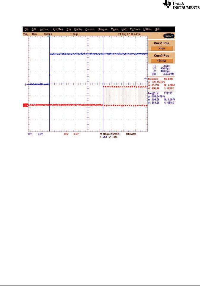
5.1.5Timing Diagrams
CHIP POWER UP TO CLOCK START
C001
Figure 5-1. Power Up [VIN (Blue) to Crystal Start (Red)]
CHIP ENABLE TO CLOCK START
C002
Figure 5-2. EN2 Low and EN High (Blue) to Start of System Clock (Red)
Copyright © 2006–2010, Texas Instruments Incorporated System Description 15
Submit Documentation Feedback
focus.ti.com: TRF7960 TRF7961
TRF7960
TRF7961
SLOU186F –AUGUST 2006–REVISED AUGUST 2010 |
www.ti.com |
CHIP ENABLE TO CLOCK START
C003
Figure 5-3. EN2 High and EN Low (Blue) to Start of System Clock (Red)
16 System Description Copyright © 2006–2010, Texas Instruments Incorporated
Submit Documentation Feedback
focus.ti.com: TRF7960 TRF7961
Loading...