


 Loading...
Texas Instruments TPS79301DBVREP, TPS79301MDBVREP, TPS79318DBVREP, TPS79325DBVREP, TPS793285DBVREP Schematic [ru]
...TPS79301-EP, TPS79318-EP, TPS79325-EP, TPS79328-EP
TPS793285-EP, TPS79330-EP, TPS79333-EP, TPS793475-EP
www.ti.com |
SGLS163B – APRIL 2003 – REVISED NOVEMBER 2006 |
|
ULTRALOW-NOISE, HIGH-PSRR, FAST RF 200-mA
LOW-DROPOUT LINEAR REGULATORS
FEATURES
∙Controlled Baseline
–One Assembly/Test Site, One Fabrication Site
∙Enhanced Diminishing Manufacturing Sources (DMS) Support
∙Enhanced Product-Change Notification
∙Qualification Pedigree (1)
∙200-mA Low-Dropout Regulator With EN
∙Available in 1.8 V, 2.5 V, 2.8 V, 2.85 V, 3 V, 3.3 V, 4.75 V, and Adjustable
∙High PSRR (70 dB at 10 kHz)
∙Ultralow Noise (32 μV)
∙Fast Start-Up Time (50 μs)
∙Stable With a 2.2-μF Ceramic Capacitor
∙Excellent Load/Line Transient
∙Very Low Dropout Voltage
(112 mV at Full Load, TPS79330)
∙5-Pin SOT23 (DBV) Package
APPLICATIONS
∙VCOs
∙RF
∙Bluetooth™, Wireless LAN
(1)Component qualification in accordance with JEDEC and industry standards to ensure reliable operation over specified temperature range. This includes, but is not limited to, Highly Accelerated Stress Test (HAST) or biased 85/85, temperature cycle, autoclave or unbiased HAST, electromigration, bond intermetallic life, and mold compound life. Such qualification testing should not be viewed as justifying use of this component beyond specified performance and environmental limits.
DBV PACKAGE
(TOP VIEW)
IN |
|
|
|
|
|
|
|
OUT |
|
|
1 |
5 |
|
|
|||
|
2 |
|
|
|
||||
GND |
|
|
|
|
|
|||
EN |
|
|
|
|
|
|
BYPASS |
|
|
|
3 |
4 |
|
|
|||
|
|
|
|
|
|
|
||
|
|
Fixed Option |
|
|||||
|
DBV PACKAGE |
|
||||||
|
|
(TOP VIEW) |
|
|||||
IN |
|
|
|
|
|
|
OUT |
|
|
|
|
|
|
|
|
||
|
1 |
|
6 |
|
|
|||
|
|
|
|
|||||
|
|
|
|
|
|
|
|
|
GND |
|
2 |
|
5 |
|
|
FB |
|
EN |
|
|
|
|
|
|
|
BYPASS |
|
3 |
|
4 |
|
|
|||
|
|
|
|
|
|
|
|
|
|
|
|
|
|
|
|
|
|
Adjustable Option
DESCRIPTION
The TPS793xx family of low-dropout (LDO) low-power linear voltage regulators features high power-supply rejection ratio (PSRR), ultralow noise, fast start-up, and excellent line and load transient responses in a small-outline SOT23 package. Each device in the family is stable, with a small 2.2-μF ceramic capacitor on the output. The TPS793xx family uses an advanced, proprietary, BiCMOS fabrication process to yield extremely low dropout voltages (e.g., 112 mV at 200 mA, TPS79330). Each device achieves fast start-up times (approximately 50 μs with a 0.001-μF bypass capacitor), while consuming very low quiescent current (170 μA typical). Moreover, when the device is placed in standby mode, the supply current is reduced to less than 1 μA. The TPS79328 exhibits approximately
32 μVRMS of output voltage noise with a 0.1-μF bypass capacitor. Applications with analog
components that are noise sensitive, such as portable RF electronics, benefit from the high PSRR and low-noise features, as well as the fast response time.
Please be aware that an important notice concerning availability, standard warranty, and use in critical applications of Texas Instruments semiconductor products and disclaimers thereto appears at the end of this data sheet.
Bluetooth is a trademark of Bluetooth SIG, Inc.
PRODUCTION DATA information is current as of publication date. |
Copyright © 2003–2006, Texas Instruments Incorporated |
Products conform to specifications per the terms of the Texas |
|
Instruments standard warranty. Production processing does not |
|
necessarily include testing of all parameters. |
|
TPS79301-EP, TPS79318-EP, TPS79325-EP, TPS79328-EP
TPS793285-EP, TPS79330-EP, TPS79333-EP, TPS793475-EP
www.ti.com
SGLS163B – APRIL 2003 – REVISED NOVEMBER 2006
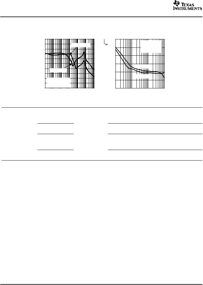
TPS79328 |
TPS79328 |
RIPPLE REJECTION
|
|
|
|
vs |
|
|
|
|
|
|
FREQUENCY |
|
|
||
|
100 |
|
|
|
|
|
|
|
90 |
|
|
|
IO = 200 mA |
|
|
|
80 |
|
|
|
|
|
|
dB |
70 |
|
|
|
|
|
|
− |
|
|
|
|
|
|
|
|
|
|
|
|
|
|
|
Rejection |
60 |
|
|
|
|
|
|
50 |
|
|
|
|
|
|
|
|
|
|
|
|
|
|
|
Ripple |
40 |
IO = 10 mA |
|
|
|
|
|
|
|
|
|
|
|||
30 |
|
|
|
|
|
|
|
|
20 |
VI = 3.8 V |
|
|
|
|
|
|
|
|
|
|
|
||
|
10 |
Co = 10 μF |
|
|
|
|
|
|
0 |
C(byp) = 0.01 μF |
|
|
|
|
|
|
10 |
100 |
1 k |
10 k |
100 k |
1 M |
10 M |
|
|
|
f − Frequency − Hz |
|
|
||
OUTPUT SPECTRAL NOISE DENSITY
|
|
|
vs |
|
|
0.3 |
FREQUENCY |
|
|
Hz |
|
|
|
|
|
|
VI = 3.8 V |
|
|
|
|
|
|
|
V/ |
0.25 |
|
Co = 2.2 μF |
|
μ |
|
|
C(byp) = 0.1 μF |
|
|
|
|
|
|
− |
0.2 |
|
|
|
Density |
|
|
|
|
0.15 |
|
|
|
|
Noise |
|
IO = 1 mA |
|
|
|
|
|
||
|
|
|
|
|
Spectral |
0.1 |
|
|
|
|
|
IO = 200 mA |
|
|
0.05 |
|
|
|
|
Output |
|
|
|
|
0 |
|
|
|
|
|
100 |
1 k |
10 k |
100 k |
|
|
f − Frequency − Hz |
|
|
TJ |
VOLTAGE |
|
|
1.2 to 5.5 V |
|
|
1.8 V |
|
|
2.5 V |
|
–40°C to 125°C |
2.8 V |
|
2.85 V |
||
|
||
|
3 V |
|
|
3.3 V |
|
|
4.75 V |
|
–55°C to 125°C |
1.2 to 5.5 V |
(1)The DBVR indicates tape and reel of 3000 parts.
(2)Product preview
AVAILABLE OPTIONS
PACKAGE |
PART NUMBER |
SYMBOL |
|
|
TPS79301DBVREP(1) |
PGVE |
|
|
TPS79318DBVREP(1) |
PHHE |
|
|
TPS79325DBVREP(1) |
PGWE |
|
SOT23 |
TPS79328DBVREP(1)(2) |
PGXE |
|
TPS793285DBVREP(1)(2) |
PHIE |
||
(DBV) |
|||
TPS79330DBVREP(1)(2) |
PGYE |
||
|
|||
|
TPS793333DBVREP(1) |
PHUE |
|
|
TPS793475DBVREP(1) |
PHJE |
|
|
TPS79301MDBVREP(1) |
PMBM |
2 |
Submit Documentation Feedback |
TPS79301-EP, TPS79318-EP, TPS79325-EP, TPS79328-EP
TPS793285-EP, TPS79330-EP, TPS79333-EP, TPS793475-EP
www.ti.com
SGLS163B – APRIL 2003 – REVISED NOVEMBER 2006
ABSOLUTE MAXIMUM RATINGS(1)
over operating free-air temperature range (unless otherwise noted)
|
|
MIN |
MAX |
UNIT |
|
Input voltage range(2) |
–0.3 |
6 |
V |
|
Voltage range at EN |
–0.3 |
VI + |
V |
|
|
|
0.3 |
|
|
Voltage on OUT |
–0.3 |
6 |
V |
|
Peak output current |
|
Internally limited |
|
|
ESD rating |
Human-Body Model (HBM) |
2 |
kV |
|
Changed-Device Model (CDM) |
500 |
V |
|
|
|
|||
|
Continuous total power dissipation |
|
See Dissipation |
|
|
|
Rating Table |
||
|
|
|
||
TJ |
Operating virtual junction temperature range |
–55 |
125 |
°C |
Tstg |
Storage temperature range |
–65 |
150 |
°C |
(1)Stresses beyond those listed under "absolute maximum ratings" may cause permanent damage to the device. These are stress ratings only, and functional operation of the device at these or any other conditions beyond those indicated under "recommended operating conditions" is not implied. Exposure to absolute-maximum-rated conditions for extended periods may affect device reliability.
(2)All voltage values are with respect to network ground terminal
Dissipation Ratings
|
|
RθJC |
RθJA |
DERATING |
TA ≤ 25°C |
TA = 70°C |
TA = 85°C |
BOARD |
PACKAGE |
FACTOR ABOVE |
POWER |
POWER |
POWER |
||
|
|
|
|
TA = 25°C |
RATING |
RATING |
RATING |
Low K(1) |
DBV |
63.75°C/W |
256°C/W |
3.906 mW/°C |
391 mW |
215 mW |
156 mW |
High K(2) |
DBV |
63.75°C/W |
178.3°C/W |
5.609 mW/°C |
561 mW |
308 mW |
224 mW |
(1)The JEDEC low K (1s) board design used to derive this data was a 3-in × 3-in, two layer board with 2-oz copper traces on top of the board.
(2)The JEDEC high K (2s2p) board design used to derive this data was a 3-in × 3-in, multilayer board with 1-oz internal power and ground planes and 2-oz copper traces on top and bottom of the board.
Submit Documentation Feedback |
3 |

TPS79301-EP, TPS79318-EP, TPS79325-EP, TPS79328-EP
TPS793285-EP, TPS79330-EP, TPS79333-EP, TPS793475-EP
www.ti.com
SGLS163B – APRIL 2003 – REVISED NOVEMBER 2006
ELECTRICAL CHARACTERISTICS
over recommended operating free-air temperature range, EN = VI, TJ = –55 to 125°C and TJ = –40 to 125°C, VI = VO(typ) + 1 V, IO = 1 mA, Co = 10 μF, C(byp) = 0.01 μF (unless otherwise noted)
|
PARAMETER |
TEST CONDITIONS |
MIN |
TYP |
MAX |
UNIT |
||
V |
Input voltage(1) |
|
|
|
2.7 |
|
5.5 |
V |
I |
|
|
|
|
|
|
|
|
I |
Continuous output current(2) |
|
|
0 |
|
200 |
mA |
|
O |
|
|
|
|
|
|
|
|
TJ |
Operating junction temperature |
|
|
–55 |
|
125 |
°C |
|
|
|
|
0 mA < IO < 200 mA, |
TJ = –40 to 125°C, |
0.98 Vo |
|
1.02 Vo |
|
|
|
|
1.22 V £ VO £ 5.2 V (3) |
|
|
|
||
|
|
TPS79301 |
|
|
|
|
|
|
|
|
0 mA < IO < 200 mA, |
TJ = –55 to 125°C, |
|
|
1.025 |
|
|
|
|
|
0.97 Vo |
|
|
|||
|
|
|
1.22 V £ VO £ 5.2 V (3) |
|
|
Vo |
|
|
|
|
|
|
|
|
|
||
|
|
TPS79318 |
TJ = 25°C |
|
|
1.8 |
|
|
|
|
0 mA < IO < 200 mA, |
2.8 V < VI < 5.5 V |
1.764 |
|
1.836 |
|
|
|
|
|
|
|
||||
|
|
TPS79325 |
TJ = 25°C |
|
|
2.5 |
|
|
|
|
0 mA < IO < 200 mA, |
3.5 V < VI < 5.5 V |
2.45 |
|
2.55 |
|
|
|
|
|
|
|
||||
|
|
TPS79328 |
TJ = 25°C |
|
|
2.8 |
|
|
Output voltage |
0 mA < IO < 200 mA, |
3.8 V < VI < 5.5 V |
2.744 |
|
2.856 |
V |
||
|
|
|||||||
|
|
TPS793285 |
TJ = 25°C |
|
|
2.85 |
|
|
|
|
0 mA < IO < 200 mA, |
3.85 V < VI < 5.5 V |
2.793 |
|
2.907 |
|
|
|
|
|
|
|
||||
|
|
TPS79330 |
TJ = 25°C |
|
|
3 |
|
|
|
|
0 mA < IO < 200 mA, |
4 V < VI < 5.5 V |
2.94 |
|
3.06 |
|
|
|
|
|
|
|
||||
|
|
TPS79333 |
TJ = 25°C |
|
|
3.3 |
|
|
|
|
0 mA < IO < 200 mA, |
4.3 V < VI < 5.5 V |
3.234 |
|
3.366 |
|
|
|
|
|
|
|
||||
|
|
TPS793475 |
TJ = 25°C |
|
|
4.75 |
|
|
|
|
0 mA < IO < 200 mA, |
5.25 V < VI < 5.5 V |
4.655 |
|
4.845 |
|
|
|
|
|
|
|
||||
Quiescent current (GND current) |
0 mA < IO < 200 mA, |
TJ = 25°C |
|
170 |
|
mA |
||
0 mA < IO < 200 mA |
|
|
|
220 |
||||
|
|
|
|
|
|
|
||
Load regulation |
|
0 mA < IO < 200 mA, |
TJ = 25°C |
|
5 |
|
mV |
|
Output voltage line regulation (DVO/VO)(4) |
VO + 1 V < VI £ 5.5 V, |
TJ = 25°C |
|
0.05 |
|
%/V |
||
VO + 1 V < VI £ 5.5 V |
|
|
|
0.12 |
||||
|
|
|
|
|
|
|
||
|
|
|
|
C(byp) = 0.001 mF |
|
55 |
|
|
Output noise voltage (TPS79328) |
BW = 200 Hz to 100 kHz, |
C(byp) = 0.0047 mF |
|
36 |
|
mVRMS |
||
IO = 200 mA, TJ = 25°C |
C(byp) = 0.01 mF |
|
33 |
|
||||
|
|
|
|
|
|
|||
|
|
|
|
C(byp) = 0.1 mF |
|
32 |
|
|
|
|
|
RL = 14 W, |
C(byp) = 0.001 mF |
|
50 |
|
|
Time, start-up (TPS79328) |
|
C(byp) = 0.0047 mF |
|
70 |
|
ms |
||
|
Co = 1 mF, TJ = 25°C |
|
|
|||||
|
|
|
C(byp) = 0.01 mF |
|
100 |
|
|
|
|
|
|
|
|
|
|
||
Output current limit |
|
V = 0 V(3) |
|
285 |
|
600 |
mA |
|
|
|
|
O |
|
|
|
|
|
Standby current |
|
EN = 0 V, |
2.7 V < VI < 5.5 V |
|
0.07 |
1 |
mA |
|
High-level enable input voltage |
2.7 V < VI < 5.5 V |
|
2 |
|
|
V |
||
Low-level enable input voltage |
2.7 V < VI < 5.5 V |
|
|
|
0.7 |
V |
||
Input current (EN) |
|
EN = 0 |
|
–1 |
|
1 |
mA |
|
(1)To calculate the minimum input voltage for your maximum output current, use the following formula: VI(min) = VO(max) + VDO (max load)
(2)Continuous output current and operating junction temperature are limited by internal protection circuitry, but it is not recommended that the device operate under conditions beyond those specified in this table for extended periods of time.
(3)The minimum IN operating voltage is 2.7 V or VO(typ) + 1 V, whichever is greater. The maximum IN voltage is 5.5 V. The maximum output current is 200 mA.
(4)If VO £ 2.5 V, then VImin = 2.7 V, VImax = 5.5 V:
Line Reg. (mV) + % V VImax * 2.7 V 1000VO
100
If VO ³ 2.5 V, then VImin = VO + 1 V, VImax = 5.5 V.
4 |
Submit Documentation Feedback |
TPS79301-EP, TPS79318-EP, TPS79325-EP, TPS79328-EP
TPS793285-EP, TPS79330-EP, TPS79333-EP, TPS793475-EP
www.ti.com
SGLS163B – APRIL 2003 – REVISED NOVEMBER 2006
ELECTRICAL CHARACTERISTICS (continued)
over recommended operating free-air temperature range, EN = VI, TJ = –55 to 125°C and TJ = –40 to 125°C, VI = VO(typ) + 1 V, IO = 1 mA, Co = 10 μF, C(byp) = 0.01 μF (unless otherwise noted)
PARAMETER
 Input current (FB) (TPS79301)
 Power-supply ripple rejection
 Dropout voltage(5)
 UVLO threshold UVLO hysteresis
TPS79328
TPS79328
TPS793285
TPS79330
TPS79333
TPS793475
TEST CONDITIONS |
MIN TYP |
MAX |
UNIT |
|
FB = 1.8 V |
|
|
1 |
μA |
f = 100 Hz, TJ = 25°C, |
IO = 10 mA |
70 |
|
|
f = 100 Hz, TJ = 25°C, |
IO = 200 mA |
68 |
|
dB |
f = 10 Hz, TJ = 25°C, |
IO = 200 mA |
70 |
|
|
|
|
|||
f = 100 Hz, TJ = 25°C, |
IO = 200 mA |
43 |
|
|
IO = 200 mA, |
TJ = 25°C |
120 |
|
|
IO = 200 mA |
|
|
200 |
|
IO = 200 mA, |
TJ= 25°C |
120 |
|
|
IO = 200 mA |
|
|
200 |
|
IO = 200 mA, |
TJ = 25°C |
112 |
|
mV |
IO = 200 mA |
|
|
200 |
|
|
|
|
||
IO = 200 mA, |
TJ = 25°C |
102 |
|
|
IO = 200 mA |
|
|
180 |
|
IO = 200 mA, |
TJ = 25°C |
77 |
|
|
IO = 200 mA |
|
|
125 |
|
VCC rising |
|
2.25 |
2.65 |
V |
TJ = 25°C |
VCC rising |
100 |
|
mV |
(5)IN voltage equals VO(typ)– 100 mV; The TPS79325 dropout voltage is limited by the input voltage range limitations.
Submit Documentation Feedback |
5 |
TPS79301-EP, TPS79318-EP, TPS79325-EP, TPS79328-EP
TPS793285-EP, TPS79330-EP, TPS79333-EP, TPS793475-EP
www.ti.com
SGLS163B – APRIL 2003 – REVISED NOVEMBER 2006
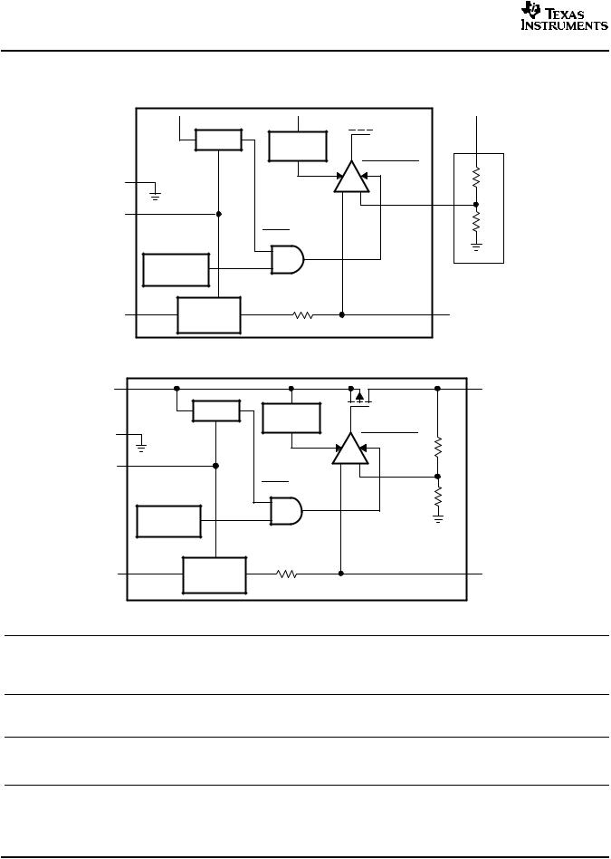
DEVICE INFORMATION
FUNCTIONAL BLOCK DIAGRAM – ADJUSTABLE VERSION
VIN 
 VOUT
VOUT
|
UVLO |
Current |
|
|
|
|
Sense |
|
|
|
|
ILIM |
SHUTDOWN |
R1 |
|
|
|
||
GND |
|
_ |
+ |
|
|
|
|||
|
|
|
|
FB |
EN |
|
|
|
|
|
|
UVLO |
|
R2 |
|
|
|
|
|
|
Thermal |
|
|
|
|
Shutdown |
|
|
External to |
|
|
|
|
the Device |
VIN |
Bandgap |
250 kΩ |
Vref |
Bypass |
Reference |
|
|
||
|
|
|
|
FUNCTIONAL BLOCK DIAGRAM – FIXED VERSION |
|
|||
VIN |
|
|
|
|
VOUT |
|
UVLO |
Current |
|
|
|
|
|
Sense |
|
|
|
GND |
|
ILIM |
|
SHUTDOWN |
|
|
|
|
R1 |
|
|
|
|
|
_ |
|
|
|
|
|
+ |
|
|
EN |
|
|
|
|
|
|
|
|
|
|
|
|
|
UVLO |
|
|
|
|
|
|
|
R2 |
|
|
Thermal |
|
|
|
|
|
Shutdown |
|
|
|
|
VIN |
Bandgap |
250 kΩ |
|
Vref |
Bypass |
Reference |
|
|
|
||
|
|
|
|
|
|
|
|
|
|
TERMINAL FUNCTIONS |
|
|
TERMINAL |
|
I/O |
DESCRIPTION |
|
NAME |
ADJ |
FIXED |
|||
|
|
||||
BYPASS |
4 |
4 |
|
An external bypass capacitor, connected to this terminal, in conjunction with an internal |
|
|
resistor, creates a low-pass filter to further reduce regulator noise. |
||||
|
|
|
|
||
EN |
3 |
3 |
I |
Enable input that enables or shuts down the device. When EN goes to a logic high, the |
|
device is enabled. When the device goes to a logic low, the device is in shutdown mode. |
|||||
|
|
|
|
||
FB |
5 |
N/A |
I |
Feedback input voltage for the adjustable device |
|
GND |
2 |
2 |
|
Regulator ground |
|
IN |
1 |
1 |
I |
Input to the device |
|
OUT |
6 |
5 |
O |
Regulated output of the device |
6 |
Submit Documentation Feedback |

TPS79301-EP, TPS79318-EP, TPS79325-EP, TPS79328-EP
TPS793285-EP, TPS79330-EP, TPS79333-EP, TPS793475-EP
www.ti.com
SGLS163B – APRIL 2003 – REVISED NOVEMBER 2006
TYPICAL CHARACTERISTICS
TPS79328
OUTPUT VOLTAGE vs
OUTPUT CURRENT
|
2.805 |
|
|
|
|
2.805 |
|
2.804 |
|
|
VI = 3.8 V |
|
|
|
|
|
Co = 10 F |
|
|
|
|
|
|
|
|
2.8 |
|
|
2.803 |
|
|
TJ = 25° C |
|
|
|
|
|
− V |
|
||
V |
2.802 |
|
|
|
|
|
Output V oltage − |
|
|
|
− Output V oltage |
2.795 |
|
|
|
|
|
|||
2.801 |
|
|
|
|
||
2.8 |
|
|
|
2.79 |
||
2.799 |
|
|
|
|
||
2.798 |
|
|
|
2.785 |
||
− |
|
|
|
O |
||
|
|
|
|
|||
O |
|
|
|
|
||
2.797 |
|
|
|
|
||
V |
|
|
|
V |
2.78 |
|
|
|
|
|
|
|
|
|
2.796 |
|
|
|
|
|
|
2.795 |
|
|
|
|
2.775 |
|
0 |
50 |
100 |
150 |
200 |
|
|
|
IO − Output Current − mA |
|
|
||
Figure 1.
TPS79328
|
TPS79328 |
|
|
|
TPS79328 |
|
|
|
||||||
OUTPUT VOLTAGE |
GROUND CURRENT |
|
||||||||||||
|
|
vs |
|
|
|
|
|
|
vs |
|
|
|
|
|
JUNCTION TEMPERATURE |
JUNCTION TEMPERATURE |
|||||||||||||
|
|
|
|
|
|
|
250 |
|
|
|
|
|
|
|
|
|
|
|
|
|
|
VI = 3.8 V |
|
|
|
|
|
|
|
|
|
|
|
|
|
A |
Co = 10 F |
|
IO = 1 mA |
|
|
|||
|
|
IO = 1 mA |
|
200 |
|
|
|
|
|
|
|
|||
|
|
|
µ |
|
|
|
|
|
|
|
|
|||
|
|
|
|
|
|
− |
|
|
|
|
|
|
|
|
|
|
|
|
|
|
Current |
150 |
|
|
IO = 200 mA |
|
|
||
|
|
|
|
|
|
|
|
|
|
|
|
|
||
|
|
|
|
|
|
|
|
|
|
|
|
|
|
|
|
IO = 200 mA |
|
|
Ground |
100 |
|
|
|
|
|
|
|
||
|
|
|
|
|
|
|
|
|
|
|
|
|
|
|
|
|
|
|
|
|
|
50 |
|
|
|
|
|
|
|
VI = 3.8 V |
|
|
|
|
|
|
|
|
|
|
|
|
|
|
Co = 10 F |
|
|
|
|
|
|
|
|
|
|
|
|
|
|
−40 −25 −10 5 |
20 |
35 |
50 |
65 |
80 |
95 110 125 |
0 |
|
|
|
|
|
|
|
−40 −25−10 5 |
20 |
35 |
50 |
65 |
80 |
95 110 125 |
||||||||
T − Junction T emperature − °C |
TJ − Junction T emperature − |
° |
||||||||||||
J |
|
|
|
|
|
|
C |
|||||||
|
|
Figure 2. |
|
|
|
|
Figure 3. |
|
|
|
||||
|
TPS79328 |
|
|
|
TPS79328 |
|
|
|
||||||
OUTPUT SPECTRAL NOISE DENSITY |
OUTPUT SPECTRAL NOISE DENSITY |
OUTPUT SPECTRAL NOISE DENSITY |
|
|
|
vs |
|
|
|
|
|
|
|
vs |
|
|
|
|
|
|
|
vs |
|
|
0.3 |
|
FREQUENCY |
|
|
|
0.3 |
|
FREQUENCY |
|
|
|
1.6 |
|
|
FREQUENCY |
|
|||
Hz |
|
|
|
|
|
Hz |
|
|
|
|
|
Hz |
|
|
|
|
|
|||
|
|
VI |
= 3.8 V |
|
|
|
|
VI = 3.8 V |
|
|
|
|
|
VI = 3.8 V |
||||||
|
|
|
|
|
|
|
|
|
|
1.4 |
|
|
|
|||||||
V/ |
|
|
C |
= 2.2 μF |
V/ |
|
|
|
C = 10 μF |
|
V/ |
|
|
|
IO = 200 mA |
|||||
0.25 |
|
o |
|
|
|
0.25 |
|
|
o |
|
|
|
|
|
|
Co= 10 μF |
||||
m |
|
C(byp) = 0.1 μF |
m |
|
|
C(byp) = 0.1 μF |
|
m |
|
|
|
|
||||||||
|
|
|
|
|
|
1.2 |
|
|
|
|||||||||||
|
|
|
|
|
|
|
|
|
|
|
|
|
|
DensityNoiseSpectralOutput− |
|
|
C(byp) = 0.001 μF |
|
||
DensityNoiseSpectralOutput− |
0 |
|
|
|
|
|
DensityNoiseSpectralOutput− |
0 |
|
|
|
|
|
0 |
|
|
|
|||
|
0.2 |
|
|
|
|
|
|
0.2 |
|
|
|
|
|
|
1 |
|
|
C(byp) = 0.0047 |
μ |
|
|
|
|
|
|
|
|
|
|
|
|
|
|
|
|
|
|
||||
|
|
|
|
|
|
|
|
|
|
|
|
|
|
|
|
|
|
F |
||
|
0.15 |
|
IO = 1 mA |
|
|
|
0.15 |
|
|
IO = 1 mA |
|
|
|
0.8 |
|
|
|
C(byp) = 0.01 μF |
||
|
|
|
|
|
|
|
|
|
|
|
|
|
|
|
|
|
|
|
||
|
0.1 |
|
|
|
|
|
|
0.1 |
|
|
|
|
|
|
0.6 |
|
|
|
C(byp) = 0.1 μF |
|
|
|
|
|
|
|
|
|
|
|
|
|
|
|
|
|
|
|
|
||
|
|
|
IO = 200 mA |
|
|
|
|
|
|
IO = 200 mA |
|
|
|
0.4 |
|
|
|
|
|
|
|
0.05 |
|
|
|
|
|
|
0.05 |
|
|
|
|
|
|
0.2 |
|
|
|
|
|
|
|
|
|
|
|
|
|
|
|
|
|
|
|
|
|
|
|
|
|
|
|
|
100 |
1 k |
10 k |
|
100 k |
|
100 |
|
1 k |
10 k |
|
100 k |
|
100 |
|
1 k |
10 k |
100 k |
|
|
|
|
f − Frequency − Hz |
|
|
|
|
|
f − Frequency − Hz |
|
|
|
|
|
|
f − Frequency − Hz |
|
|||
|
|
|
Figure 4. |
|
|
|
|
|
|
Figure 5. |
|
|
|
|
|
|
Figure 6. |
|
||
|
ROOT MEAN SQUARED OUTPUT NOISE |
|
|
OUTPUT IMPEDANCE |
|
|
|
|
|
TPS79328 |
|
|||||||||
(RMS) |
|
|
vs |
|
|
|
|
|
|
|
vs |
|
|
|
|
|
|
DROPOUT VOLTAGE |
||
|
|
BYPASS CAPACITANCE |
|
|
|
FREQUENCY |
|
|
|
|
|
|
|
vs |
|
|||||
60 |
|
|
|
|
|
|
2.5 |
|
|
|
|
|
|
|
JUNCTION TEMPERATURE |
|||||
V |
|
|
VO = 2.8 V |
|
VI = 3.8 V |
|
|
|
|
|
180 |
|
|
|
|
|
||||
m |
|
|
|
|
|
|
|
|
|
|
|
|
|
|||||||
|
|
IO = 200 mA |
|
Co = 10 F |
|
|
|
|
|
VI = 2.7 V |
|
|
||||||||
|
50 |
|
|
|
|
|
|
|
|
|
||||||||||
OutputSquaredNoise − |
|
Co = 10 |
μ |
F |
ImpedanceOutput− − Ω |
TJ = 25° C |
|
|
|
|
160 |
C |
o |
= 10 F |
|
|
||||
|
|
|
2 |
|
|
|
|
|
oltageVDropout− mV |
|
|
|
|
|
||||||
40 |
|
|
|
|
|
|
|
|
|
|
|
140 |
|
|
|
|
|
|||
|
|
|
|
|
|
|
|
|
|
|
|
|
|
|
|
|
||||
|
|
|
|
|
|
|
|
1.5 |
|
|
|
|
|
|
120 |
|
|
|
IO = 200 mA |
|
|
|
|
|
|
|
|
|
|
IO = 1 mA |
|
|
|
|
|
|
|
||||
|
30 |
|
|
|
|
|
|
|
|
|
|
|
100 |
|
|
|
|
|
||
|
|
|
|
|
|
|
|
|
|
|
|
|
|
|
|
|
|
|
||
|
|
|
|
|
|
|
|
|
|
|
|
|
|
|
|
|
|
|
|
|
|
20 |
|
|
|
|
|
|
1 |
|
|
|
|
|
|
80 |
|
|
|
|
|
|
|
|
|
|
|
|
|
|
|
|
|
|
|
|
|
|
|
|
||
|
|
|
|
|
|
|
IO = 100 mA |
|
|
|
|
|
|
|
|
|
|
|||
Mean |
|
|
|
|
|
|
Z |
|
|
|
DO |
40 |
|
|
|
|
|
|||
|
|
|
|
|
|
|
o |
0.5 |
|
|
|
|
|
− |
60 |
|
|
|
|
|
|
10 |
|
|
|
|
|
|
|
|
|
|
|
|
|
|
|
|
|||
Root− |
|
|
|
|
|
|
|
|
|
|
|
|
|
|
|
|
|
|
|
|
|
BW = 100 Hz to 100 |
|
|
|
|
|
|
|
|
|
|
V |
20 |
|
|
IO = 10 mA |
|
|||
|
|
|
|
|
|
|
|
|
|
|
|
|
|
|
|
|
|
|
||
RMS |
0 |
kHz |
|
|
|
|
0 |
|
|
|
|
|
|
|
|
|
|
|
|
|
0.001 |
0.01 |
|
|
0.1 |
|
10 |
100 |
1 k |
10 k 100 k |
1 M |
10 M |
|
0 |
|
|
|
50 65 80 |
95 110 125 |
||
|
|
|
C(byp) − Bypass Capacitance − |
μF |
|
|
|
f − Frequency − Hz |
|
|
|
−40 −25−10 5 20 35 |
||||||||
|
|
|
|
|
|
|
|
|
|
|
|
|
|
|
|
|
|
TJ − Junction T emperature − °C |
||
|
|
|
Figure 7. |
|
|
|
|
|
|
Figure 8. |
|
|
|
|
|
|
Figure 9. |
|
||
Submit Documentation Feedback |
7 |
Loading...