


 Loading...
Texas Instruments TVP3010-135MGAB, TVP3010-135MGA, TVP3010-135FN, TVP3010-110FN, TVP3010-85FNR Datasheet
...TVP3010C, TVP3010M
Data Manual
Video Interface Palette
SLAS082A
October 1997
Printed on Recycled Paper

IMPORTANT NOTICE
Texas Instruments (TI) reserves the right to make changes to its products or to discontinue any semiconductor product or service without notice, and advises its customers to obtain the latest version of relevant information to verify, before placing orders, that the information being relied on is current.
TI warrants performance of its semiconductor products and related software to the specifications applicable at the time of sale in accordance with TI's standard warranty. Testing and other quality control techniques are utilized to the extent TI deems necessary to support this warranty. Specific testing of all parameters of each device is not necessarily performed, except those mandated by government requirements.
Certain applications using semiconductor products may involve potential risks of death, personal injury, or severe property or environmental damage (ªCritical Applicationsº).
TI SEMICONDUCTOR PRODUCTS ARE NOT DESIGNED, INTENDED, AUTHORIZED, OR WARRANTED TO BE SUITABLE FOR USE IN LIFE-SUPPORT APPLICATIONS, DEVICES OR SYSTEMS OR OTHER CRITICAL APPLICATIONS.
Inclusion of TI products in such applications is understood to be fully at the risk of the customer. Use of TI products in such applications requires the written approval of an appropriate TI officer. Questions concerning potential risk applications should be directed to TI through a local SC sales office.
In order to minimize risks associated with the customer's applications, adequate design and operating safeguards should be provided by the customer to minimize inherent or procedural hazards.
TI assumes no liability for applications assistance, customer product design, software performance, or infringement of patents or services described herein. Nor does TI warrant or represent that any license, either express or implied, is granted under any patent right, copyright, mask work right, or other intellectual property right of TI covering or relating to any combination, machine, or process in which such semiconductor products or services might be or are used.
Copyright 1997, Texas Instruments Incorporated

Contents
Section |
Title |
Page |
1 Introduction . . . . . . . . . . . . . . . . . . . . . . . . . . . . . . . . . . . . . . . . . . . . . . . . . . . . . . . . . . . . . . . 1±1
1.1 Features (TVP3010C and TVP3010M) . . . . . . . . . . . . . . . . . . . . . . . . . . . . . . . . . . . . 1±3 1.2 Functional Block Diagram . . . . . . . . . . . . . . . . . . . . . . . . . . . . . . . . . . . . . . . . . . . . . . . 1±4 1.3 Terminal Assignments . . . . . . . . . . . . . . . . . . . . . . . . . . . . . . . . . . . . . . . . . . . . . . . . . . 1±5 1.4 Ordering Information . . . . . . . . . . . . . . . . . . . . . . . . . . . . . . . . . . . . . . . . . . . . . . . . . . . 1±7 1.5 Terminal Functions (TVP3010C and TVP3010M) . . . . . . . . . . . . . . . . . . . . . . . . . . . 1±7
2 Detailed Description . . . . . . . . . . . . . . . . . . . . . . . . . . . . . . . . . . . . . . . . . . . . . . . . . . . . . . . 2±1
2.1 MPU Interface . . . . . . . . . . . . . . . . . . . . . . . . . . . . . . . . . . . . . . . . . . . . . . . . . . . . . . . . . 2±1 2.2 Color Palette . . . . . . . . . . . . . . . . . . . . . . . . . . . . . . . . . . . . . . . . . . . . . . . . . . . . . . . . . . 2±4 2.2.1 Writing to Color-Palette RAM . . . . . . . . . . . . . . . . . . . . . . . . . . . . . . . . . . . . 2±4 2.2.2 Reading From Color-Palette RAM . . . . . . . . . . . . . . . . . . . . . . . . . . . . . . . 2±4 2.2.3 Palette Page Register . . . . . . . . . . . . . . . . . . . . . . . . . . . . . . . . . . . . . . . . . . 2±4 2.2.4 Read Masking . . . . . . . . . . . . . . . . . . . . . . . . . . . . . . . . . . . . . . . . . . . . . . . . 2±5
2.3Clock Selection and Output-Clock (SCLK, RCLK, and VCLK) Generation . . . . . 2±5
2.3.1 RCLK, SCLK, VCLK . . . . . . . . . . . . . . . . . . . . . . . . . . . . . . . . . . . . . . . . . . . 2±5 2.3.2 Frame-Buffer Clocking: Self-Clocked or Externally Clocked . . . . . . . . . 2±8 2.4 Multiplexing Scheme . . . . . . . . . . . . . . . . . . . . . . . . . . . . . . . . . . . . . . . . . . . . . . . . . . 2±12 2.4.1 Little-Endian and Big-Endian Data Format . . . . . . . . . . . . . . . . . . . . . . . 2±12 2.4.2 VGA Pass-Through Mode . . . . . . . . . . . . . . . . . . . . . . . . . . . . . . . . . . . . . 2±13 2.4.3 Pseudo-Color Mode . . . . . . . . . . . . . . . . . . . . . . . . . . . . . . . . . . . . . . . . . . 2±13 2.4.4 Direct-Color Mode . . . . . . . . . . . . . . . . . . . . . . . . . . . . . . . . . . . . . . . . . . . . 2±13 2.4.5 True-Color Mode . . . . . . . . . . . . . . . . . . . . . . . . . . . . . . . . . . . . . . . . . . . . . 2±14 2.4.6 Multiplex Control Registers . . . . . . . . . . . . . . . . . . . . . . . . . . . . . . . . . . . . 2±22
2.5 On-Chip Cursor . . . . . . . . . . . . . . . . . . . . . . . . . . . . . . . . . . . . . . . . . . . . . . . . . . . . . . . 2±23 2.5.1 Cursor RAM . . . . . . . . . . . . . . . . . . . . . . . . . . . . . . . . . . . . . . . . . . . . . . . . . 2±23 2.5.2 Two-Color 64 ×64 Cursor . . . . . . . . . . . . . . . . . . . . . . . . . . . . . . . . . . . . . 2±24 2.5.3 64 ×64 Cursor Positioning . . . . . . . . . . . . . . . . . . . . . . . . . . . . . . . . . . . . . 2±24 2.5.4 Crosshair Cursor . . . . . . . . . . . . . . . . . . . . . . . . . . . . . . . . . . . . . . . . . . . . . 2±25 2.5.5 Dual-Cursor Positioning . . . . . . . . . . . . . . . . . . . . . . . . . . . . . . . . . . . . . . . 2±26
2.6 Auxiliary Window, Port Select, and Color-Key Switching . . . . . . . . . . . . . . . . . . . . 2±27 2.6.1 Windowing Control . . . . . . . . . . . . . . . . . . . . . . . . . . . . . . . . . . . . . . . . . . . 2±28 2.6.2 Color-Key-Switching Control . . . . . . . . . . . . . . . . . . . . . . . . . . . . . . . . . . . 2±30 2.7 Overscan . . . . . . . . . . . . . . . . . . . . . . . . . . . . . . . . . . . . . . . . . . . . . . . . . . . . . . . . . . . . 2±31
2.8 Horizontal Zooming . . . . . . . . . . . . . . . . . . . . . . . . . . . . . . . . . . . . . . . . . . . . . . . . . . . 2±32 2.9 Test Functions . . . . . . . . . . . . . . . . . . . . . . . . . . . . . . . . . . . . . . . . . . . . . . . . . . . . . . . . 2±33 2.9.1 16-Bit CRC . . . . . . . . . . . . . . . . . . . . . . . . . . . . . . . . . . . . . . . . . . . . . . . . . . 2±33 2.9.2 Sense-Comparator Output and Test Register . . . . . . . . . . . . . . . . . . . . . 2±33 2.9.3 Identification Code (ID) Register . . . . . . . . . . . . . . . . . . . . . . . . . . . . . . . . 2±34 2.10 MUXOUT [SENSE]Output . . . . . . . . . . . . . . . . . . . . . . . . . . . . . . . . . . . . . . . . . . . . . 2±34
iii

Section |
|
Title |
Page |
2.11 |
Reset . . |
. . . . . . . . . . . . . . . . . . . . . . . . . . . . . . . . . . . . . . . . . . . . . . . . . . . . . . . . . . . . . |
2±34 |
|
2.11.1 |
Power-On Reset . . . . . . . . . . . . . . . . . . . . . . . . . . . . . . . . . . . . . . . . . . . . . |
2±34 |
|
2.11.2 |
Software Reset . . . . . . . . . . . . . . . . . . . . . . . . . . . . . . . . . . . . . . . . . . . . . . . |
2±34 |
2.12 |
Frame-Buffer Interface . . . . . . . . . . . . . . . . . . . . . . . . . . . . . . . . . . . . . . . . . . . . . . . . |
2±35 |
|
2.13 |
Analog-Output Specifications . . . . . . . . . . . . . . . . . . . . . . . . . . . . . . . . . . . . . . . . . . . |
2±35 |
|
2.14 |
Video Control: Horizontal Sync, Vertical Sync, and Blank . . . . . . . . . . . . . . . . . . . |
2±37 |
|
2.15 |
Split Shift Register Transfer VRAMs . . . . . . . . . . . . . . . . . . . . . . . . . . . . . . . . . . . . . |
2±37 |
|
2.16 |
Control Register Definitions . . . . . . . . . . . . . . . . . . . . . . . . . . . . . . . . . . . . . . . . . . . . |
2±38 |
|
|
2.16.1 |
Configuration Register . . . . . . . . . . . . . . . . . . . . . . . . . . . . . . . . . . . . . . . . |
2±38 |
|
2.16.2 |
General Control Register . . . . . . . . . . . . . . . . . . . . . . . . . . . . . . . . . . . . . . |
2±39 |
|
2.16.3 |
Cursor Control Register . . . . . . . . . . . . . . . . . . . . . . . . . . . . . . . . . . . . . . . |
2±40 |
|
2.16.4 |
Cursor Position X and Y Registers . . . . . . . . . . . . . . . . . . . . . . . . . . . . . . |
2±41 |
|
2.16.5 |
Sprite Origin X and Y Registers . . . . . . . . . . . . . . . . . . . . . . . . . . . . . . . . |
2±42 |
|
2.16.6 |
Window Start X and Y Registers . . . . . . . . . . . . . . . . . . . . . . . . . . . . . . . . |
2±43 |
|
2.16.7 |
Window Stop X and Y Registers . . . . . . . . . . . . . . . . . . . . . . . . . . . . . . . . |
2±44 |
|
2.16.8 |
Cursor Color 0, 1 RGB Registers . . . . . . . . . . . . . . . . . . . . . . . . . . . . . . . |
2±45 |
|
2.16.9 |
Cursor-RAM Address Register . . . . . . . . . . . . . . . . . . . . . . . . . . . . . . . . . |
2±46 |
|
2.16.10 |
Cursor RAM Data Register . . . . . . . . . . . . . . . . . . . . . . . . . . . . . . . . . . . . |
2±46 |
|
2.16.11 |
AuxiliaryControl Register . . . . . . . . . . . . . . . . . . . . . . . . . . . . . . . . . . . . . . |
2±47 |
|
2.16.12 |
Color-Key-Control Register . . . . . . . . . . . . . . . . . . . . . . . . . . . . . . . . . . . . |
2±48 |
|
2.16.13 |
Color-Key (Red, Green, Blue, Overlay) Low and High Registers . . . . |
2±49 |
|
2.16.14 |
Overscan Color RGB Registers . . . . . . . . . . . . . . . . . . . . . . . . . . . . . . . . |
2±50 |
|
2.16.15 |
CRC LSB and MSB Registers . . . . . . . . . . . . . . . . . . . . . . . . . . . . . . . . . . |
2±51 |
|
2.16.16 |
CRC Control Register . . . . . . . . . . . . . . . . . . . . . . . . . . . . . . . . . . . . . . . . . |
2±51 |
3 Electrical Characteristics . . . . . . . . . . . . . . . . . . . . . . . . . . . . . . . . . . . . . . . . . . . . . . . . . . 3±1
3.1 Absolute Maximum Ratings Over Operating Free-Air Temperature Range . . . . 3±1 3.2 Recommended Operating Conditions . . . . . . . . . . . . . . . . . . . . . . . . . . . . . . . . . . . . . 3±1
3.3Electrical Characteristics for TVP3010C Over Recommended Ranges of
Supply Voltage and Operating Free-Air Temperature . . . . . . . . . . . . . . . . . . . . . . . 3±2
3.4Electrical Characteristics for TVP3010M Over Recommended Ranges of
Supply Voltage and Operating Free-Air Temperature . . . . . . . . . . . . . . . . . . . . . . . 3±3 3.5 Operating Characteristics (TVP3010C) . . . . . . . . . . . . . . . . . . . . . . . . . . . . . . . . . . . 3±4 3.6 Operating Characteristics (TVP3010M) . . . . . . . . . . . . . . . . . . . . . . . . . . . . . . . . . . . 3±5 3.7 Timing Requirements (TVP3010C) . . . . . . . . . . . . . . . . . . . . . . . . . . . . . . . . . . . . . . . 3±6 3.8 Timing Requirements (TVP3010M) . . . . . . . . . . . . . . . . . . . . . . . . . . . . . . . . . . . . . . . 3±7
3.9Switching Characteristics for TVP3010C Over Recommended Ranges of
Supply Voltage and Operating Free-Air Temperature . . . . . . . . . . . . . . . . . . . . . . . 3±8 3.10 Switching Characteristics for TVP3010M Over Recommended Ranges of
Supply Voltage and Operating Free-Air Temperature . . . . . . . . . . . . . . . . . . . . . . 3±10 3.11 Timing Diagrams . . . . . . . . . . . . . . . . . . . . . . . . . . . . . . . . . . . . . . . . . . . . . . . . . . . . . . 3±11
iv

Section |
Title |
Page |
Appendix A Printed Circuit Board Layout Considerations . . . . . . . . . . . . . . . . . . . . . A±1 Appendix B RCLK Frequency < VCLK Frequency . . . . . . . . . . . . . . . . . . . . . . . . . . . . . B±1 Appendix C Little-Endian and Big-Endian Data Formats . . . . . . . . . . . . . . . . . . . . . . . C±1 Appendix D Examples: Register Settings . . . . . . . . . . . . . . . . . . . . . . . . . . . . . . . . . . . . . D±1 Appendix E Mechanical Data . . . . . . . . . . . . . . . . . . . . . . . . . . . . . . . . . . . . . . . . . . . . . . . . E±1
List of Illustrations
Figure |
Title |
Page |
2±1 |
Dot Clock/VCLK/RCLK/SCLK Relationship . . . . . . . . . . . . . . . . . . . . . . . . . . . . . . . |
. 2±7 |
2±2 |
SCLK/VCLK Control Timing |
|
|
(SSRT Disabled, RCLK/SCLK Frequency = VCLK Frequency) . . . . . . . . . . . . . . . . |
2±8 |
2±3 |
SCLK/VCLK Control Timing |
|
|
(SSRT Enabled, RCLK/SCLK Frequency = VCLK Frequency) . . . . . . . . . . . . . . . . |
2±9 |
2±4 |
SCLK/VCLK Control Timing |
|
|
(SSRT Disabled, RCLK/SCLK Frequency = 4 x VCLK Frequency) . . . . . . . . . . . . |
2±10 |
2±5 |
SCLK/VCLK Control Timing |
|
|
(SSRT Enabled, RCLK/SCLK Frequency = 4 x VCLK Frequency) . . . . . . . . . . . . |
2±10 |
2±6 |
CursorRAM Organization . . . . . . . . . . . . . . . . . . . . . . . . . . . . . . . . . . . . . . . . . . . . . . . |
2±24 |
2±7 |
Common Sprite-Origin Settings . . . . . . . . . . . . . . . . . . . . . . . . . . . . . . . . . . . . . . . . . . |
2±25 |
2±8 |
Dual-Cursor Positioning . . . . . . . . . . . . . . . . . . . . . . . . . . . . . . . . . . . . . . . . . . . . . . . . . |
2±26 |
2±9 |
One Possible Custom-Cursor Creation . . . . . . . . . . . . . . . . . . . . . . . . . . . . . . . . . . . . |
2±26 |
2±10 |
VGA in the Auxiliary Window . . . . . . . . . . . . . . . . . . . . . . . . . . . . . . . . . . . . . . . . . . . . |
2±29 |
2±11 |
Multiple VGA Windows Using Port Select (PSEL) . . . . . . . . . . . . . . . . . . . . . . . . . . |
2±30 |
2±12 |
Overscan . . . . . . . . . . . . . . . . . . . . . . . . . . . . . . . . . . . . . . . . . . . . . . . . . . . . . . . . . . . . . |
2±32 |
2±13 |
Equivalent Circuit of the Current Output (IOG) . . . . . . . . . . . . . . . . . . . . . . . . . . . . . |
2±35 |
2±14 |
Composite Video Output (With 0 IRE, 8-Bit Output) . . . . . . . . . . . . . . . . . . . . . . . . . |
2±36 |
2±15 |
Composite Video Output (With 7.5 IRE, 8-Bit Output) . . . . . . . . . . . . . . . . . . . . . . . |
2±36 |
2±16 |
Split Shift Register Transfer Timing . . . . . . . . . . . . . . . . . . . . . . . . . . . . . . . . . . . . . . . |
2±37 |
3±1 |
MPU Interface Timing . . . . . . . . . . . . . . . . . . . . . . . . . . . . . . . . . . . . . . . . . . . . . . . . . . . |
3±11 |
3±2 |
Video Input/Output Timing . . . . . . . . . . . . . . . . . . . . . . . . . . . . . . . . . . . . . . . . . . . . . . |
3±12 |
3±3 |
SFLAG Timing (When SSRT Function is Enabled) . . . . . . . . . . . . . . . . . . . . . . . . . . |
3±13 |
v

List of Tables
Table |
Title |
Page |
2±1 |
Direct Register Map . . . . . . . . . . . . . . . . . . . . . . . . . . . . . . . . . . . . . . . . . . . . . . . . . . . |
. . 2±1 |
2±2 |
Indirect Register Map (Extended Registers) . . . . . . . . . . . . . . . . . . . . . . . . . . . . . . . |
. 2±2 |
2±3 |
Allocation of Palette-Page Register Bits . . . . . . . . . . . . . . . . . . . . . . . . . . . . . . . . . . . |
. 2±5 |
2±4 |
Input-Clock-Selection Register . . . . . . . . . . . . . . . . . . . . . . . . . . . . . . . . . . . . . . . . . . . |
. 2±7 |
2±5 |
Output-Clock-Selection Register Format . . . . . . . . . . . . . . . . . . . . . . . . . . . . . . . . . . |
. 2±6 |
2±6 |
Multiplex Mode and Bus-Width Selection . . . . . . . . . . . . . . . . . . . . . . . . . . . . . . . . . . |
2±15 |
2±7 |
Pseudo-Color Mode Pixel-Latching Sequence . . . . . . . . . . . . . . . . . . . . . . . . . . . . . |
2±18 |
2±8 |
Direct-Color Mode Pixel-Latching Sequence (Little Endian) . . . . . . . . . . . . . . . . . . |
2±19 |
2±9 |
Direct-Color Mode Pixel-Latching Sequence (Big Endian) . . . . . . . . . . . . . . . . . . . |
2±20 |
2±10 |
True-Color Mode Pixel-Latching Sequence (Little Endian) . . . . . . . . . . . . . . . . . . . |
2±21 |
2±11 |
True-Color Mode Pixel-Latching Sequence (Big Endian) . . . . . . . . . . . . . . . . . . . . |
2±22 |
2±12 |
Two-Color 64 ×64 Cursor-RAM Selection . . . . . . . . . . . . . . . . . . . . . . . . . . . . . . . . . |
2±24 |
2±13 |
Crosshair-Cursor Color Selection . . . . . . . . . . . . . . . . . . . . . . . . . . . . . . . . . . . . . . . . |
2±25 |
2±14 |
Cursor-Intersection Truth Table . . . . . . . . . . . . . . . . . . . . . . . . . . . . . . . . . . . . . . . . . . |
2±27 |
2±15 |
Windowing Control . . . . . . . . . . . . . . . . . . . . . . . . . . . . . . . . . . . . . . . . . . . . . . . . . . . . . |
2±28 |
2±16 |
Zoom Control . . . . . . . . . . . . . . . . . . . . . . . . . . . . . . . . . . . . . . . . . . . . . . . . . . . . . . . . . . |
2±32 |
2±17 |
Sense-Test Register . . . . . . . . . . . . . . . . . . . . . . . . . . . . . . . . . . . . . . . . . . . . . . . . . . . . |
2±34 |
2±18 |
K1 and K2 Values Defined . . . . . . . . . . . . . . . . . . . . . . . . . . . . . . . . . . . . . . . . . . . . . . |
2±36 |
2±19 |
Configuration Register . . . . . . . . . . . . . . . . . . . . . . . . . . . . . . . . . . . . . . . . . . . . . . . . . . |
2±38 |
2±20 |
General Control Register . . . . . . . . . . . . . . . . . . . . . . . . . . . . . . . . . . . . . . . . . . . . . . . . |
2±39 |
2±21 |
Cursor Control Register . . . . . . . . . . . . . . . . . . . . . . . . . . . . . . . . . . . . . . . . . . . . . . . . . |
2±40 |
2±22 |
Cursor Position X (LSB) and X (MSB) . . . . . . . . . . . . . . . . . . . . . . . . . . . . . . . . . . . . . |
2±41 |
2±23 |
Sprite Origin X and Y Registers . . . . . . . . . . . . . . . . . . . . . . . . . . . . . . . . . . . . . . . . . . |
2±42 |
2±24 |
Window Start X and Y Registers . . . . . . . . . . . . . . . . . . . . . . . . . . . . . . . . . . . . . . . . . |
2±43 |
2±25 |
Window Stop X and Y Registers . . . . . . . . . . . . . . . . . . . . . . . . . . . . . . . . . . . . . . . . . |
2±44 |
2±26 |
Cursor-Color RGB Registers . . . . . . . . . . . . . . . . . . . . . . . . . . . . . . . . . . . . . . . . . . . . |
2±45 |
2±27 |
Cursor RAM Address Register . . . . . . . . . . . . . . . . . . . . . . . . . . . . . . . . . . . . . . . . . . . |
2±46 |
2±28 |
Cursor RAM Data Register . . . . . . . . . . . . . . . . . . . . . . . . . . . . . . . . . . . . . . . . . . . . . . |
2±46 |
2±29 |
Auxiliary-Control Register . . . . . . . . . . . . . . . . . . . . . . . . . . . . . . . . . . . . . . . . . . . . . . . |
2±47 |
2±30 |
Color-Key Control Register . . . . . . . . . . . . . . . . . . . . . . . . . . . . . . . . . . . . . . . . . . . . . . |
2±48 |
2±31 |
Color-Key Low and High Registers . . . . . . . . . . . . . . . . . . . . . . . . . . . . . . . . . . . . . . . |
2±49 |
2±32 |
Overscan-Color RGB Register . . . . . . . . . . . . . . . . . . . . . . . . . . . . . . . . . . . . . . . . . . . |
2±50 |
2±33 |
CRC MSB and LSB Registers . . . . . . . . . . . . . . . . . . . . . . . . . . . . . . . . . . . . . . . . . . . |
2±51 |
2±34 |
CRC Control Register Format . . . . . . . . . . . . . . . . . . . . . . . . . . . . . . . . . . . . . . . . . . . . |
2±51 |
vi

1 Introduction
The TVP3010C and the TVP3010M palettes are commercial and military versions, respectively, of an advanced Video Interface Palette (VIP) from Texas Instruments implemented in the EPIC 0.8-micron CMOS process. Differences between the two versions are outlined in separate tables. In both versions, maximum flexibility is provided by the pixel multiplexing scheme. The scheme accommodates 64-, 32-, 16-, 8-, and 4-bit pixel buses without any circuit modification. This enables the system to be easily reconfigured for varying amounts of available video RAM. The device supports selection of littleor big-endian data format for the pixel-bus/frame-buffer interface. Data can be split into 1, 2, 4, or 8 bit-planes for pseudo-color mode or split into 12-, 16or 24-bit true-color and direct-color modes. For the 24-bit direct-color modes, an 8-bit overlay plane is available. The 16-bit direct-color and true-color modes can be configured to IBM XGA (5, 6, 5), TARGA (5, 5, 5, 1), or (6, 6, 4) as another existing format. An additional 12-bit mode (4, 4, 4, 4) is supported with 4 bits for each color and overlay. An on-chip, IBM XGA-compatible hardware cursor is incorporated so that further increases in graphics-system performance are possible. Both devices are software compatible with the INMOS IMSG176/8 and Brooktree Bt476/8 color palettes.
An internal-frequency doubler is incorporated, allowing convenient and cost-effective clock-source alternatives to be utilized. An auxiliary windowing function and a pixel-port select function are provided so that overlay or VGA graphics can be displayed on top of direct color inside or outside a specified auxiliary window. Color-keyed switching of direct color and overlay is also supported.
Clocking is provided through one of five TTL inputs, CLK0±CLK4, and is software selectable. Additionally, CLK1/CLK2 and CLK3/CLK4 can be selected as differential ECL clock sources. The video, shift-clock, and reference-clock outputs provide a software-selected divide ratio of the chosen clock input. The reference clock can optionally be provided as an output on CLK3, and a data-latch clock can optionally be input on CLK4.
The TVP3010C and the TVP3010M have three 256 8 color look-up tables with triple 8-bit video digital-to-analog converters (DACs) capable of directly driving a doubly-terminated 75-Ω line. The lookup tables are designed with a dual-ported RAM architecture that enables ultra-high speed operation. Sync generation is incorporated on the green output channel. Horizontal sync and vertical sync are fed through the device and optionally inverted to indicate screen resolution to the monitor. A palette-page register provides the additional bits of palette address when 1, 2, or 4 bit-planes are used. This allows the screen colors to be changed with only one microprocessor-interface unit (MPU) write cycle.
Each device features a separate VGA bus that allows data from the feature connector of most VGA-supported personal computers to be fed directly into the palette without the need for external data multiplexing. This allows a replacement graphics board to remain downwards compatible by utilizing the existing graphics circuitry often located on the motherboard.
Both the TVP3010 VIP and the TVP3010M VIP are highly system integrated. Either device can be connected to the serial port of a VRAM device without external buffer logic and each device can be connected to many graphics engines directly. The split shift register transfer function, which is supported by VRAM, is also supported by the TVP3010C and TVP3010M.
The system-integration concept is carried to manufacturing testing and field diagnosis levels. To support these testing and diagnostic levels, several highly-integrated test functions have been designed to enable simplified testing of the palette, the graphics board, and the graphics system.
EPIC is a trademark of Texas Instruments Incorporated.
XGA is a registered trademark of International Business Machines Corporation.
TARGA is a registered trademark of Truevision Incorporated.
INMOS is a trademark of INMOS International Limited.
Brooktree is a trademark of Brooktree Corporation.
1±1

The TVP3010C and TVP3010M are 32-bit devices and both are pin compatible with the TLC3407X VIP, allowing convenient performance upgrades when using devices in the TI Video Interface Palette family.
NOTE:
The TVP3010C and TVP3010M include circuits that are patented as well as circuit designs that have patents pending.
1±2

1.1Features (TVP3010C and TVP 3010M)
•Second-Generation Video Interface Palette
•Supports System Resolutions of:
±1600 × 1280 × 1, 2, 4, 8, 16 Bits/Pixel @ 60-Hz Refresh Rate
±1280 × 1024 × 1, 2, 4, 8, 16 Bits/Pixel @ 60-Hz and 72-Hz Refresh Rate
± 1024 × 768 × 1, 2, 4, 8, 16, 24 Bits/Pixel @ 60-Hz and 72-Hz Refresh Rate
±And Lower Resolutions
•Direct-Color Modes:
±24-Bit/Pixel With 8-Bit Overlay
±16-Bit/Pixel (5, 6, 5) XGA Configuration
±16-Bit/Pixel (6, 6, 4) Configuration
±15-Bit/Pixel With 1-Bit Overlay (5, 5, 5, 1) TARGA Configuration
±12-Bit/Pixel With 4-Bit Overlay (4, 4, 4, 4)
•True-Color Modes:
±24-Bit/Pixel With Gamma Correction
±16-Bit/Pixel (5, 6, 5) XGA Configuration With Gamma Correction
±16-Bit/Pixel (6, 6, 4) Configuration With Gamma Correction
±15-Bit/Pixel (5, 5, 5) TARGA Configuration With Gamma Correction
±12-Bit/Pixel (4, 4, 4) With Gamma Correction
•RCLK/SCLK/LCLK Data Latching Mechanism to Allow Flexible Control of VRAM Timing
•Direct Interfacing to Video RAM
•Support for Split Shift Register Transfers
•Supports 64-Bit-Wide Pixel Bus
•On-Chip Hardware Cursor:
±64 × 64 × 2 Cursor (XGA Functionally Compatible)
±Full-Window Crosshair
±Dual-Cursor Mode
•85-,110-,135-, and 170-MHz Versions
•Supports Overscan for Creation of Custom Screen Borders
•Versatile Pixel Bus Interface to Support Littleand Big-Endian Data Formats
•Windowed-Overlay and VGA Capability
•Color-Keyed Switching of Direct Color and Overlay
•On-Chip Clock Selection
•Internal Frequency Doubler
•Triple 8-Bit D/A Converters
•Analog Output Comparators
•Triple 256 × 8 Color-Palette RAMs
•RS-343A Compatible Outputs
•Direct VGA Pass-Through Capability
•Palette-Page Register
•Horizontal Zooming Capability
•Software Downward Compatible With IMSG176/8 and Bt476/8
•Directly to Graphics Processors
•EPIC 0.8-µm CMOS Process
1±3

1.2Functional Block Diagram
The following functional block diagram applies to both the TVP3010C and TVP3010M.
|
|
|
|
|
|
|
|
|
|
|
|
|
|
|
|
REF |
|
|
|
|
|
|
|
|
|
24 |
|
|
|
|
|
|
|
Vref |
|
FS ADJUST |
|
|
|
|
|
|
|
8 ± 8 ± 8 |
|
12 - 24 |
|
|
|
|
1.235 V |
|
|
|||
|
|
|
|
|
|
|
|
|
|
|
|
|
|
|||||
|
|
|
|
|
|
16 |
|
|
|
|
|
|
|
|
|
|
||
|
|
|
|
|
|
6 ± 6 ± 4 |
|
|
|
|
|
|
|
|
|
|
||
|
|
|
|
|
|
|
Stuffing |
|
|
|
Direct-Color |
|
|
|
|
|||
|
|
|
|
True-Color |
16 |
|
|
|
|
|
|
|
|
|||||
|
|
|
|
5 ± 6 ± 5 |
|
|
|
|
|
|
|
|
||||||
|
|
32 |
32 |
|
Logic |
|
|
Pipeline Delay |
|
|
|
|
||||||
P(0 ± 31) |
Input |
Multiplexer |
5 ± 5 ± 5 |
15 |
|
24 |
24 |
24 |
|
|
||||||||
|
|
|
|
|
|
|
|
COMP |
||||||||||
32 |
Latch |
|
|
|
|
4 ± 4 ± 4 |
12 |
|
|
|
|
|
|
|
|
|
|
|
|
|
|
|
|
|
|
|
|
|
|
|
|
|
|
|
|
|
|
|
|
|
32 Pseudo- |
|
|
|
|
|
|
8 |
|
256 ×8 |
|
|
|
|
||
|
|
|
|
Color |
|
|
|
|
|
|
|
8 |
Red |
8 |
|
|
|
|
|
|
|
|
MUX |
2 |
|
|
|
|
|
|
8 |
RAM |
|
DAC |
IOR |
||
|
|
|
|
|
Read |
|
Page |
|
|
|
|
|
||||||
|
|
|
|
1:1 |
4 |
|
|
|
|
|
|
256 ×8 |
|
|
8 |
|
||
|
|
|
|
8 |
Mask |
8 |
Reg |
8 |
|
|
|
|
|
|
||||
|
|
|
|
2:1 |
8 |
|
8 |
|
Green |
|
|
|
|
|||||
|
Input |
|
|
|
|
|
|
|
|
8 |
8 |
|
|
|
||||
VGA(0 ± 7) |
|
|
4:1 |
|
|
|
|
|
|
|
RAM |
|
|
|
||||
|
|
|
|
|
|
|
|
|
8 |
|
|
|
||||||
8 |
Latch |
8 |
|
8:1 |
|
|
|
|
|
|
|
|
|
256 ×8 |
|
|
|
|
|
|
|
|
16:1 |
|
|
|
|
|
|
|
8 |
|
Blue |
8 |
|
|
|
|
|
|
|
32:1 |
|
|
|
|
|
|
|
8 |
8 |
RAM |
Output |
DAC |
IOG |
|
|
|
|
|
|
|
|
|
|
|
|
|
|
1 ×24 |
|
MUX |
8 |
|
|
|
|
|
|
|
|
|
|
|
8 |
24 |
|
|
|
|
|
|||
|
|
|
|
|
|
|
|
|
64 ×64 |
|
|
|
|
|
||||
|
|
|
|
|
|
|
|
|
|
Cursor |
|
|
|
|
||||
|
|
|
|
|
|
|
|
|
|
|
|
24 |
|
|
|
|||
|
|
|
|
|
|
Frequency |
|
|
|
|
Cursor |
|
Color 0 |
|
|
|
||
|
|
|
|
|
|
|
Color-Key |
|
|
|
|
|
|
|||||
|
|
|
|
|
|
|
|
RAM |
|
1 ×24 |
|
|
|
|
||||
|
|
|
|
|
|
Doubler |
|
Switch |
|
|
|
|
|
|
||||
|
|
|
|
|
|
|
|
and |
|
Cursor |
24 |
|
|
|
||||
|
|
|
|
|
|
|
|
|
|
|
|
|
|
|
|
|||
|
|
|
|
|
|
|
|
|
|
|
|
Control |
|
Color 1 |
|
DAC |
IOB |
|
|
|
|
|
|
|
|
|
|
|
|
|
|
|
|
||||
|
|
|
|
|
|
|
|
|
|
|
|
|
|
|
|
|
||
|
|
|
|
|
|
|
|
|
|
|
|
|
|
1 ×24 |
|
|
8 |
|
|
|
|
|
|
|
|
|
|
|
|
|
|
|
|
|
|
|
|
D(0 ± 7) |
|
|
|
|
|
|
|
|
|
|
|
|
|
Overscan |
24 |
|
|
|
8 |
|
|
|
|
|
|
|
|
|
|
|
|
|
|
|
|
|
|
RS(0 ± 2) |
MPU |
|
|
|
|
|
|
|
|
|
|
|
|
|
|
|
|
|
Registers |
|
|
|
|
|
|
|
|
|
|
|
|
2 |
|
|
Test Function |
|
|
3 |
and |
|
|
Clock Select |
|
|
|
|
|
|
|
|
|
|
and |
|
||
|
|
|
|
|
|
|
|
|
|
|
|
|
|
|||||
RD |
Control |
|
|
|
and |
|
|
|
|
|
|
|
|
|
|
Sense Comparator |
|
|
|
|
|
|
|
|
|
|
|
|
|
|
|
|
|
||||
|
Logic |
|
|
|
Control |
|
|
|
|
|
|
|
|
|
|
|
MUXOUT [SENSE] |
|
WR |
|
|
|
|
|
|
|
|
|
|
|
|
|
Auxiliary Window |
|
|||
|
|
|
|
|
|
|
|
|
|
|
|
|
Video-Signal |
HSYNCOUT |
||||
|
|
|
|
|
2 |
|
|
|
|
|
|
|
|
and |
|
|||
|
|
|
|
|
|
|
|
|
|
|
|
Port Select |
Control |
VSYNCOUT |
||||
|
|
|
|
|
|
|
|
|
|
|
|
|
|
|||||
CLK0 |
CLK1/CLK2 |
SFLAG |
CLK3 [LCLK] |
CLK3 [RCLK] SCLK VCLK |
8/6 [OVS] |
RS3 [PSEL] |
HSYNC |
|
VSYNC |
SYSBL |
VGABL |
|
|||||||||||
|
|
||||||||||
|
|
|
|
|
|
|
|||||
|
|
|
|
|
|
|
|
|
|
1±4
1.3Terminal Assignments
84-PIN PLCC PACKAGE
P18 P19 P20 P21 P22 P23 P24 P25 P26 P27 P28 |
P29 P30 |
P31 DV |
GND SCLK |
VCLK CLK0 CLK1 CLK2 |
|
|
DD |
|
|
|
|
|
|
|
|
|
|
|
|
|
|
|
|
|
|
|
|
|
|
|
|
|
|
|
|
|
|
|
|
|
|
|
|
|
|
|
|
|
|
|
|
|
|
|
|
|
|
|
|
|
P17 |
|
11 10 |
9 |
|
8 |
|
7 |
|
6 |
|
5 |
|
4 |
|
3 |
|
2 |
|
1 |
|
84 83 82 81 80 79 |
78 77 76 75 |
|
|
|
|||||||||||||||||||||||||
|
|
|
|
|
|
|
|
|
|
|
||||||||||||||||||||||||||||||||||||||||
|
12 |
|
|
|
|
|
|
|
|
|
|
|
|
|
|
|
|
|
|
|
|
|
|
|
|
|
|
|
|
|
|
|
|
|
74 |
|
||||||||||||||
|
|
|
|
|
|
|
|
|
|
|
|
|
|
|
|
|
|
|
|
|
|
|
|
|
|
|
|
|
|
|
|
|
|
|
||||||||||||||||
P16 |
|
13 |
|
|
|
|
|
|
|
|
|
|
|
|
|
|
|
|
|
|
|
|
|
|
|
|
|
|
|
|
|
|
|
|
|
73 |
|
|||||||||||||
|
|
|
|
|
|
|
|
|
|
|
|
|
|
|
|
|
|
|
|
|
|
|
|
|
|
|
|
|
|
|
|
|
|
|
||||||||||||||||
P15 |
|
14 |
|
|
|
|
|
|
|
|
|
|
|
|
|
|
|
|
|
|
|
|
|
|
|
|
|
|
|
|
|
|
|
|
|
72 |
|
|||||||||||||
|
|
|
|
|
|
|
|
|
|
|
|
|
|
|
|
|
|
|
|
|
|
|
|
|
|
|
|
|
|
|
|
|
|
|
||||||||||||||||
P14 |
|
15 |
|
|
|
|
|
|
|
|
|
|
|
|
|
|
|
|
|
|
|
|
|
|
|
|
|
|
|
|
|
|
|
|
|
71 |
|
|||||||||||||
|
|
|
|
|
|
|
|
|
|
|
|
|
|
|
|
|
|
|
|
|
|
|
|
|
|
|
|
|
|
|
|
|
|
|
||||||||||||||||
P13 |
|
16 |
|
|
|
|
|
|
|
|
|
|
|
|
|
|
|
|
|
|
|
|
|
|
|
|
|
|
|
|
|
|
|
|
|
70 |
|
|||||||||||||
|
|
|
|
|
|
|
|
|
|
|
|
|
|
|
|
|
|
|
|
|
|
|
|
|
|
|
|
|
|
|
|
|
|
|
||||||||||||||||
P12 |
|
17 |
|
|
|
|
|
|
|
|
|
|
|
|
|
|
|
|
|
|
|
|
|
|
|
|
|
|
|
|
|
|
|
|
|
69 |
|
|||||||||||||
|
|
|
|
|
|
|
|
|
|
|
|
|
|
|
|
|
|
|
|
|
|
|
|
|
|
|
|
|
|
|
|
|||||||||||||||||||
P11 |
|
18 |
|
|
|
|
|
|
|
|
|
|
|
|
|
|
|
|
|
|
|
|
|
|
|
|
|
|
|
|
|
|
|
|
|
68 |
|
|||||||||||||
|
|
|
|
|
|
|
|
|
|
|
|
|
|
|
|
|
|
|
|
|
|
|
|
|
|
|
|
|
|
|
|
|||||||||||||||||||
P10 |
|
19 |
|
|
|
|
|
|
|
|
|
|
|
|
|
|
|
|
|
|
|
|
|
|
|
|
|
|
|
|
|
|
|
|
|
67 |
|
|||||||||||||
|
|
|
|
|
|
|
|
|
|
|
|
|
|
|
|
|
|
|
|
|
|
|
|
|
|
|
|
|
|
|
|
|||||||||||||||||||
|
|
P9 |
|
20 |
|
|
|
|
|
|
|
|
|
|
|
|
|
|
|
|
|
|
|
|
|
|
|
|
|
|
|
|
|
|
|
|
|
66 |
|
|||||||||||
|
|
|
|
|
|
|
|
|
|
|
|
|
|
|
|
|
|
|
|
|
|
|
|
|
|
|
|
|
|
|
|
|
|
|||||||||||||||||
|
|
P8 |
|
21 |
|
|
|
|
|
|
|
|
|
|
|
|
|
|
|
|
|
|
|
|
|
|
|
|
|
|
|
|
|
|
|
|
|
65 |
|
|||||||||||
|
|
|
|
|
|
|
|
|
|
|
|
|
|
|
|
|
|
|
|
|
|
|
|
|
|
|
|
|
|
|
|
|
|
|||||||||||||||||
|
|
P7 |
|
22 |
|
|
|
|
|
|
|
|
|
|
|
|
|
|
|
|
|
|
|
|
|
|
|
|
|
|
|
|
|
|
|
|
|
64 |
|
|||||||||||
|
|
|
|
|
|
|
|
|
|
|
|
|
|
|
|
|
|
|
|
|
|
|
|
|
|
|
|
|
|
|
|
|
|
|||||||||||||||||
|
|
P6 |
|
23 |
|
|
|
|
|
|
|
|
|
|
|
|
|
|
|
|
|
|
|
|
|
|
|
|
|
|
|
|
|
|
|
|
|
63 |
|
|||||||||||
|
|
|
|
|
|
|
|
|
|
|
|
|
|
|
|
|
|
|
|
|
|
|
|
|
|
|
|
|
|
|
|
|
|
|||||||||||||||||
|
|
P5 |
|
24 |
|
|
|
|
|
|
|
|
|
|
|
|
|
|
|
|
|
|
|
|
|
|
|
|
|
|
|
|
|
|
|
|
|
62 |
|
|||||||||||
|
|
|
|
|
|
|
|
|
|
|
|
|
|
|
|
|
|
|
|
|
|
|
|
|
|
|
|
|
|
|
|
|
|
|||||||||||||||||
|
|
P4 |
|
25 |
|
|
|
|
|
|
|
|
|
|
|
|
|
|
|
|
|
|
|
|
|
|
|
|
|
|
|
|
|
|
|
|
|
61 |
|
|||||||||||
|
|
|
|
|
|
|
|
|
|
|
|
|
|
|
|
|
|
|
|
|
|
|
|
|
|
|
|
|
|
|
|
|
|
|||||||||||||||||
|
|
P3 |
|
26 |
|
|
|
|
|
|
|
|
|
|
|
|
|
|
|
|
|
|
|
|
|
|
|
|
|
|
|
|
|
|
|
|
|
60 |
|
|||||||||||
|
|
|
|
|
|
|
|
|
|
|
|
|
|
|
|
|
|
|
|
|
|
|
|
|
|
|
|
|
|
|
|
|
|
|||||||||||||||||
|
|
P2 |
|
27 |
|
|
|
|
|
|
|
|
|
|
|
|
|
|
|
|
|
|
|
|
|
|
|
|
|
|
|
|
|
|
|
|
|
59 |
|
|||||||||||
|
|
|
|
|
|
|
|
|
|
|
|
|
|
|
|
|
|
|
|
|
|
|
|
|
|
|
|
|
|
|
|
|
|
|||||||||||||||||
|
|
P1 |
|
28 |
|
|
|
|
|
|
|
|
|
|
|
|
|
|
|
|
|
|
|
|
|
|
|
|
|
|
|
|
|
|
|
|
|
58 |
|
|||||||||||
|
|
|
|
|
|
|
|
|
|
|
|
|
|
|
|
|
|
|
|
|
|
|
|
|
|
|
|
|
|
|
|
|
|
|||||||||||||||||
|
|
P0 |
|
|
29 |
|
|
|
|
|
|
|
|
|
|
|
|
|
|
|
|
|
|
|
|
|
|
|
|
|
|
|
|
|
|
|
|
|
57 |
|
||||||||||
|
|
|
|
|
|
|
|
|
|
|
|
|
|
|
|
|
|
|
|
|
|
|
|
|
|
|
|
|
|
|
|
|
|
|
|
|
|
|||||||||||||
|
|
|
|
|
|
30 |
|
|
|
|
|
|
|
|
|
|
|
|
|
|
|
|
|
|
|
|
|
|
|
|
|
|
|
|
|
|
|
|
|
56 |
|
|||||||||
|
WR |
|
|
|
|
|
|
|
|
|
|
|
|
|
|
|
|
|
|
|
|
|
|
|
|
|
|
|
|
|
|
|
|
|
|
|
|
|||||||||||||
|
|
|
|
|
|
|
|
|
|
|
|
|
|
|
|
|
|
|
|
|
|
|
|
|
|
|
|
|
|
|
|
|
|
|
|
|
||||||||||||||
|
|
|
|
|
|
31 |
|
|
|
|
|
|
|
|
|
|
|
|
|
|
|
|
|
|
|
|
|
|
|
|
|
|
|
|
|
|
|
|
|
55 |
|
|||||||||
|
|
RD |
|
|
|
|
|
|
|
|
|
|
|
|
|
|
|
|
|
|
|
|
|
|
|
|
|
|
|
|
|
|
|
|
|
|
||||||||||||||
|
|
|
|
|
|
|
|
|
|
|
|
|
|
|
|
|
|
|
|
|
|
|
|
|
|
|
|
|
|
|
|
|
|
|
|
|
|
|
||||||||||||
RS0 |
|
|
32 |
|
|
|
|
|
|
|
|
|
|
|
|
|
|
|
|
|
|
|
|
|
|
|
|
|
|
|
|
|
|
|
|
|
54 |
|
||||||||||||
|
|
|
|
|
|
|
|
|
|
|
|
|
|
|
|
|
|
|
|
|
|
|
|
|
|
|
|
|
|
|
|
|
|
|
|
|||||||||||||||
|
|
|
|
|
|
33 |
34 35 36 37 38 39 40 41 42 43 44 45 46 47 48 49 50 51 52 53 |
|
|
|||||||||||||||||||||||||||||||||||||||||
|
|
|
|
|
|
|
|
|
|
|
|
|
|
|
|
|
|
|
|
|
|
|
|
|
|
|
|
|
|
|
|
|
|
|
|
|
|
|
|
|
|
|
|
|
|
|
|
|
|
|
|
|
|
|
|
|
|
RS1 |
RS2 |
RS3[PSEL] |
D0 |
D1 |
D2 |
D3 |
D4 |
D5 |
D6 |
D7 |
GND DV HSYNCOUT VSYNCOUT IOR IOG |
|
IOB ADJUSTFS COMP REF |
|
|||||||||||||||||||||||||||||
|
|
|
|
|
|
|
|
|
|
|
|
|
|
|
|
|
|
|
|
|
|
|
|
|
|
|
|
|
|
|
DD |
|
|
|
|
|
|
|
|
|
|
|
||||||||
CLK3[RCLK]
CLK3[LCLK]
VGA7
VGA6
VGA5
VGA4
VGA3
VGA2
VGA1
VGA0
8/6[OVS]
MUXOUT [SENSE] SFLAG
VGABL
SYSBL
VSYNC
HSYNC
AVDD
GND
AVDD
GND
1±5

1.3Terminal Assignments (continued)
84-PIN GA PACKAGE (TOP VIEW)
12 |
RS0 |
|
D0 |
D1 |
D3 |
|
D5 |
D7 |
AVDD |
HSYNC- |
IOR |
IOB |
|
|
FS |
|
|
REF |
|||||||||||
|
|
OUT |
ADJUST |
|
|
||||||||||||||||||||||||
|
|
|
|
|
|
|
|
|
|
|
|
|
|
|
|
|
|
|
|
|
|||||||||
|
|
|
|
|
|
|
|
|
|
|
|
|
|
|
|
|
|
|
|
|
|
|
|
|
|
|
|
|
|
|
|
|
|
RS2 |
RS3 |
D2 |
|
D4 |
D6 |
|
VSYNC- |
IOG |
COMP |
|
|
|
|
|
|
|
|
|
|
|
|
|
|
||
11 |
|
WR |
|
GND |
|
AVDD |
|
|
DVDD |
||||||||||||||||||||
|
|
OUT |
|
|
|
||||||||||||||||||||||||
|
|
|
|
|
|
|
[PSEL] |
|
|
|
|
|
|
|
|
|
|
|
|
|
|
|
|
|
|
|
|
|
|
|
|
|
|
|
|
|
|
|
|
|
|
|
|
|
|
|
|
|
|
|
|
|
|
|
|
|
|
|
|
|
|
|
|
|
|
|
|
|
|
|
|
|
|
|
|
|
|
|
|
|
|
|
|
|
|
|
|
|
|
|
|
P0 |
|
|
RS1 |
|
|
|
|
|
|
|
GND |
|
GND |
|
|
|
|
|
|
||||||||
10 |
|
|
RD |
|
|
|
|
|
|
|
|
|
|
HSYNC |
|
|
|||||||||||||
|
|
|
|
|
|
|
|
|
|
|
|
|
|
|
|
|
|
|
|
|
|
|
|
|
|
|
|
|
|
|
|
P2 |
|
P1 |
|
|
|
|
|
|
|
|
|
|
|
|
|
|
|
|
|
|
|
|
|
||||
9 |
|
|
|
|
|
|
|
|
|
|
|
VSYNC |
|
|
|
|
SYSBL |
|
|
||||||||||
|
|
|
|
|
|
|
|
|
|
|
|
|
|
|
|
|
|
|
|
|
|
|
|
|
|
|
|
|
|
8 |
|
P4 |
|
P3 |
|
|
|
|
|
|
|
|
|
|
|
|
SFLAG |
||||||||||||
|
|
|
|
|
|
|
|
|
|
|
|
VGABL |
|
|
|||||||||||||||
|
|
|
|
|
|
|
|
|
|
|
|
|
|
|
|
|
|
|
|
|
|
|
|
|
|
|
|
|
|
|
|
|
|
|
|
|
|
|
|
|
|
|
|
|
|
|
|
|
|
|
|
|
|
|
|
|
|
|
|
|
|
P6 |
|
P5 |
|
|
|
|
|
|
|
|
|
8/6 |
|
|
|
|
|
|
|
|
|
|
|||||
7 |
|
|
|
|
|
|
|
|
|
|
|
|
|
|
|
MUXOUT |
|||||||||||||
|
|
|
|
|
|
|
|
|
|
|
|
|
[OVS] |
||||||||||||||||
|
|
|
|
|
|
|
|
|
|
|
|
|
|
|
|
|
|
[SENSE] |
|||||||||||
|
|
|
|
|
|
|
|
|
|
|
|
|
|
|
|
|
|
|
|
|
|
|
|
||||||
|
|
|
|
|
|
|
|
|
|
|
|
|
|
|
|
|
|
|
|
|
|
|
|
|
|
|
|
|
|
6 |
|
P8 |
|
P7 |
|
|
|
|
|
|
|
|
|
|
VGA1 |
|
|
VGA0 |
|||||||||||
|
|
|
|
|
|
|
|
|
|
|
|
|
|
|
|
|
|
|
|
|
|
|
|
|
|
|
|
|
|
5 |
|
P9 |
P10 |
|
|
|
|
|
|
|
|
|
|
VGA3 |
|
|
VGA2 |
||||||||||||
|
|
|
|
|
|
|
|
|
|
|
|
|
|
|
|
|
|
|
|
|
|
|
|
|
|
|
|
|
|
4 |
P11 |
P12 |
|
|
(ESD symbol or alignment |
|
|
|
|
VGA5 |
|
|
VGA4 |
||||||||||||||||
|
|
|
|
|
|
|
|
|
|
dot on top) |
|
|
|
|
|
|
|
|
|
|
|
|
|
|
|
|
|
|
|
|
|
|
|
|
|
|
|
|
|
|
|
|
|
|
|
|
|
|
|
|
|
|
|
|
|
|
|
|
|
|
|
|
|
|
|
|
|
|
|
|
|
|
|
|
|
|
|
||||||||||||
3 |
P13 |
P15 |
P17 |
|
|
|
|
|
|
|
CLK2 |
|
|
CLK3 |
|
|
|
|
VGA6 |
||||||||||
|
|
|
|
|
|
|
|
|
|
|
|
|
|
|
|
|
[LCLK] |
|
|
|
|
|
|
||||||
|
|
|
|
|
|
|
|
|
|
|
|
|
|
|
|
|
|
|
|
|
|
|
|
|
|
|
|
|
|
2 |
P14 |
P16 |
P19 |
P22 |
|
P24 |
P27 |
P29 |
P31 |
GND |
CLK0 |
|
CLK1 |
|
|
VGA7 |
|||||||||||||
|
|
|
|
|
|
|
|
|
|
|
|
|
|
|
|
|
|
|
|
|
|
|
|
|
|
|
|
|
|
1 |
P18 |
P20 |
P21 |
P23 |
|
P25 |
P26 |
P28 |
P30 |
AVDD |
SCLK |
|
VCLK |
|
|
CLK3 |
|||||||||||||
|
|
|
|
[RCLK] |
|||||||||||||||||||||||||
|
|
|
|
|
|
|
|
|
|
|
|
|
|
|
|
|
|
|
|
|
|
|
|
|
|
||||
|
|
|
|
|
|
|
|
|
|
|
|
|
|
|
|
|
|
|
|
|
|
|
|
|
|
|
|
|
|
|
|
A |
B |
C |
D |
|
E |
F |
G |
H |
J |
K |
|
|
L |
|
|
M |
|||||||||||
1±6

1.4Ordering Information
TVP3010 XXX ± X ± XX
Pixel Clock Frequency Indicator Must contain three letters:
±85: 85-MHz pixel clock ±110: 110-MHz pixel clock ±135: 135-MHz pixel cock ±170: 170-MHz pixel clock
Military Extension M
Commercial Extension C
Package
Must contain two Letters:
FN: square plastic J-leaded chip carrier
GA: 84-pin (12 x 12) ceramic pin-grid array
1.5Terminal Functions (TVP3010C and TVP3010M)
|
|
|
TERMINAL |
|
I/O |
DESCRIPTION |
||
|
NAME |
NO. (FN) |
NO. (GA) |
|||||
|
|
|
|
|
||||
|
|
|
|
|
|
|
|
|
|
AVDD |
55, 57 |
J1, L11, G12 |
|
Analog power. All AVDD terminals must be connected. |
|||
|
CLK0 |
77 |
K2 |
I |
Dot clock 0 input. CLK0 can be selected to drive the dot |
|||
|
|
|
|
|
(TTL |
clock at frequencies up to 140 MHz. When VGA mode is |
||
|
|
|
|
|
compatible) |
active, the default clock source is CLK0. The maximum |
||
|
|
|
|
|
|
frequency in VGA mode is 85 MHz. |
||
|
|
|
|
|
|
|
|
|
|
CLK1, CLK2 |
75, 76 |
L2, K3 |
I |
Dual-mode dot clock input. These inputs are essentially |
|||
|
|
|
|
|
(TTL/ECL |
ECL-compatible inputs, but two TTL clocks may be used |
||
|
|
|
|
|
compatible) |
on the CLK1 and CLK2 if so selected in the input clock |
||
|
|
|
|
|
|
select register. These inputs may be selected as the dot |
||
|
|
|
|
|
|
clock up to the device limit while in the ECL mode or up to |
||
|
|
|
|
|
|
140 MHz in the TTL mode. |
||
|
|
|
|
|
|
|
|
|
|
CLK3[RCLK] |
74 |
M1 |
I/O |
Dot clock 3 TTL input or reference clock output. When |
|||
|
|
|
|
|
|
configured as CLK3, this terminal is similar to CLK0 and |
||
|
|
|
|
|
|
can be selected to drive the dot clock at frequencies up to |
||
|
|
|
|
|
|
140 MHz. When configured as RCLK, this terminal outputs |
||
|
|
|
|
|
|
the reference clock signal, which is similar to the SCLK |
||
|
|
|
|
|
|
signal but not gated off during blanking. This signal can be |
||
|
|
|
|
|
|
used for pixel-port timing reference or other system |
||
|
|
|
|
|
|
synchronization. The terminal defaults to CLK3 after reset. |
||
|
|
|
|
|
|
|
|
|
|
|
|
73 |
L3 |
I |
Dot clock 4 TTL input or pixel-port latch clock. |
|
|
|
CLK3[LCLK] |
CLK3[LCLK] |
||||||
|
|
|
|
|
|
can be configured to drive dot clock frequencies up to 140 |
||
|
|
|
|
|
|
MHz, or it can be configured as a latch-clock input to latch |
||
|
|
|
|
|
|
pixel-port input data. It defaults to CLK4 after reset, and |
||
|
|
|
|
|
|
LCLK is internally connected to RCLK to latch pixel-port |
||
|
|
|
|
|
|
data. |
||
|
|
|
|
|
|
|||
|
COMP |
52 |
K11 |
I |
Compensation. COMP provides compensation for the |
|||
|
|
|
|
|
|
internal reference amplifier. A 0.1- F ceramic capacitor is |
||
|
|
|
|
|
|
required between COMP and AVDD. The COMP capacitor |
||
|
|
|
|
|
|
must be as close to the device as possible to avoid noise |
||
|
|
|
|
|
|
pick up. |
||
|
|
|
|
|
|
|
|
|
NOTE 1: All unused inputs should be tied to a logic level and not be allowed to float.
1±7

1.5Terminal Functions (TVP3010C and TVP3010M) Continued
|
|
|
TERMINAL |
|
I/O |
|
DESCRIPTION |
|||
|
NAME |
NO. (FN) |
NO. (GA) |
|
||||||
|
|
|
|
|
||||||
|
|
|
|
|
|
|
|
|
|
|
|
DVDD |
45, 81 |
M11 |
|
Digital power. All DVDD terminals must be connected |
|||||
|
|
|
|
|
|
|
|
together. |
||
|
|
|
|
|
|
|
|
|
|
|
|
D(0 ± 7) |
36± 43 |
B12, C12, |
I/O |
MPU interface data bus. Data terminals are used to |
|||||
|
|
|
|
|
|
D11, D12, |
(TTL |
transfer data in and out of the register map and |
||
|
|
|
|
|
|
E11, E12, |
compatible) |
palette/overlay RAM. |
||
|
|
|
|
|
|
F11, F12 |
|
|
|
|
|
|
|
|
|
|
|
|
|
|
|
|
FS ADJUST |
51 |
L12 |
I |
Full-scale adjustment. A resistor connected between |
|||||
|
|
|
|
|
|
|
|
FS ADJUST and ground controls the full-scale range |
||
|
|
|
|
|
|
|
|
of the DACs. |
||
|
|
|
|
|
|
|
|
|
|
|
|
GND |
44, 54, |
J2, L10, |
|
Ground. All GND terminals must be connected. The |
|||||
|
|
|
|
|
56, 80 |
K10, G11 |
|
GNDs are connected internally. |
||
|
|
|
|
|
|
|
|
|
|
|
|
HSYNCOUT |
46 |
H12 |
O |
Horizontal sync output after pipeline delay. For |
|||||
|
|
|
|
|
|
|
(TTL |
system mode the horizontal-sync output can be |
||
|
|
|
|
|
|
|
compatible) |
programmed, but for the VGA mode the output |
||
|
|
|
|
|
|
|
|
carries the same polarity as the input. |
||
|
|
|
|
|
|
|
|
|
|
|
|
IOR, IOG, IOB |
48, 49, 50 |
J12, J11, |
O |
Analog current outputs. These outputs can drive a |
|||||
|
|
|
|
|
|
K12 |
|
37.5-Ω load directly (doubly terminated 75-Ω line), |
||
|
|
|
|
|
|
|
|
thus eliminating the requirement for any external |
||
|
|
|
|
|
|
|
|
buffering. |
||
|
|
|
|
|
|
|
|
|
|
|
|
|
|
|
|
63 |
M7 |
O |
Multiplexer output control or DAC comparator output |
||
|
MUXOUT |
|
[SENSE] |
|
||||||
|
|
|
|
|
|
|
(TTL |
signal. When MUXOUT is configured as a multi- |
||
|
|
|
|
|
|
|
compatible) |
plexer output control, it is software programmable |
||
|
|
|
|
|
|
|
|
through the configuration register. When the |
||
|
|
|
|
|
|
|
|
multiplexer control register is set to VGA mode, this |
||
|
|
|
|
|
|
|
|
output terminal and corresponding configuration |
||
|
|
|
|
|
|
|
|
register bit are set low to indicate to external devices |
||
|
|
|
|
|
|
|
|
that the VGA pass-through mode is being used. |
||
|
|
|
|
|
|
|
|
Alternatively, |
SENSE |
can be configured as the DAC |
|
|
|
|
|
|
|
|
comparator output. In this case, the SENSE is low |
||
|
|
|
|
|
|
|
|
when one or more of the DAC output analog levels is |
||
|
|
|
|
|
|
|
|
above the internal comparator reference of 350 mV |
||
|
|
|
|
|
|
|
|
" 50 mV. |
||
|
|
|
|
|
|
|||||
|
P(0 ± 31) |
1 ± 29, |
A10, B9, A9, |
I |
Pixel input port. The port can be used in various |
|||||
|
|
|
|
|
82± 84 |
B8, A8, B7, |
(TTL |
modes as shown in the multiplexer control register. |
||
|
|
|
|
|
|
A7, B6, A6, |
compatible) |
All the unused terminals need to be tied to GND. |
||
|
|
|
|
|
|
A5, B5, A4, |
|
|
|
|
|
|
|
|
|
|
B4, A3, A2, |
|
|
|
|
|
|
|
|
|
|
B3, B2, C3, |
|
|
|
|
|
|
|
|
|
|
A1, C2, B1, |
|
|
|
|
|
|
|
|
|
|
C1, D2, D1, |
|
|
|
|
|
|
|
|
|
|
E2, E1, F1, |
|
|
|
|
|
|
|
|
|
|
F2, G1, G2, |
|
|
|
|
|
|
|
|
|
|
H1, H2 |
|
|
|
|
NOTE 1: All unused inputs should be tied to a logic level and not be allowed to float.
1±8

1.5Terminal Functions (TVP3010C and TVP3010M) Continued
|
|
|
|
|
|
TERMINAL |
|
I/O |
|
|
DESCRIPTION |
||||
|
|
NAME |
NO. (FN) |
NO. (GA) |
|
|
|||||||||
|
|
|
|
|
|
|
|
|
|
||||||
|
|
|
|
|
|
|
|
|
|
|
|
|
|
|
|
|
REF |
53 |
M12 |
|
Voltage reference for DACs. An internal voltage reference |
||||||||||
|
|
|
|
|
|
|
|
|
of nominally 1.235 V is provided, which requires an |
||||||
|
|
|
|
|
|
|
|
|
external 0.1- F ceramic capacitor between REF and |
||||||
|
|
|
|
|
|
|
|
|
analog GND. However, the internal reference voltage can |
||||||
|
|
|
|
|
|
|
|
|
be overdriven by an externally supplied reference voltage. |
||||||
|
|
|
|
|
|
|
|
|
A typical connection is shown in Appendix A. |
||||||
|
|
|
|
|
|
|
|
|
|
|
|
|
|
|
|
|
|
|
|
|
|
31 |
B10 |
I |
Read strobe inputs When cleared to 0, |
|
initiates a |
||||
|
RD |
|
|
|
|
RD |
|||||||||
|
|
|
|
|
|
|
|
(TTL |
read from the register map. Reads are performed |
||||||
|
|
|
|
|
|
|
|
compatible) |
asynchronously and are initiated on the low-going edge of |
||||||
|
|
|
|
|
|
|
|
|
RD (see Figure 3±1). |
||||||
|
|
|
|
|
|
|
|
|
|
|
|
|
|||
|
RS(0 ± 2) |
32± 34 |
A12, C10, |
I |
Register-select inputs. The RS terminals specify the |
||||||||||
|
|
|
|
|
|
|
B11 |
(TTL |
location in the register map that is to be accessed (see |
||||||
|
|
|
|
|
|
|
|
compatible) |
Table 2±1). |
||||||
|
|
|
|
|
|
|
|
|
|
|
|
|
|||
|
RS3 [PSEL] |
35 |
C11 |
I |
Register-select input or port-select input. When configured |
||||||||||
|
|
|
|
|
|
|
|
(TTL |
as the RS3 input, this terminal has no effect. When |
||||||
|
|
|
|
|
|
|
|
compatible) |
configured as the port-select input, RS3 [PSEL] allows the |
||||||
|
|
|
|
|
|
|
|
|
creation of VGA or overlay windows in a direct-color |
||||||
|
|
|
|
|
|
|
|
|
background on a pixel-by-pixel basis. |
||||||
|
|
|
|
|
|
|
|
|
|
|
|
|
|||
|
SCLK |
79 |
K1 |
O |
Shift clock output. SCLK is selected as a division of the dot |
||||||||||
|
|
|
|
|
|
|
|
(TTL |
clock input. The output signals are gated off during |
||||||
|
|
|
|
|
|
|
|
compatible) |
blanking, although SCLK is still used internally to |
||||||
|
|
|
|
|
|
|
|
|
synchronize with the activation of Blank. |
||||||
|
|
|
|
|
|
|
|
|
|
|
|
|
|||
|
SFLAG |
62 |
M8 |
I |
Split shift register transfer flag. The TVP3010 detects a |
||||||||||
|
|
|
|
|
|
|
|
(TTL |
low-to-high transition on SFLAG during a blanking |
||||||
|
|
|
|
|
|
|
|
compatible) |
sequence and immediately generates an SCLK pulse. This |
||||||
|
|
|
|
|
|
|
|
|
early SCLK pulse replaces the first SCLK pulse in the |
||||||
|
|
|
|
|
|
|
|
|
normal sequence. |
||||||
|
|
|
|
|
|
|
|
|
|
|
|
||||
|
|
|
|
|
|
60 |
M9 |
I |
System blank input. |
|
|
is active (low). |
|||
|
SYSBL |
|
|
|
SYSBL |
||||||||||
|
|
|
|
|
|
|
|
(TTL |
|
|
|
|
|
|
|
|
|
|
|
|
|
|
|
compatible) |
|
|
|
|
|
|
|
|
|
|
|
|
|
|
|
|
|
|
|
||||
|
|
|
58, 59 |
M10, L9 |
I |
Horizontal and vertical sync inputs. These signals |
|||||||||
|
HSYNC |
, |
|||||||||||||
|
VSYNC |
|
|
(TTL |
generate the sync level on the green current output. They |
||||||||||
|
|
|
|
|
|
|
|
compatible) |
are active (low) inputs, but the HSYNCOUT and |
||||||
|
|
|
|
|
|
|
|
|
VSYNCOUT outputs can be programmed through the |
||||||
|
|
|
|
|
|
|
|
|
general control register. |
||||||
|
|
|
|
|
|
|
|
|
|||||||
|
VCLK |
78 |
L1 |
O |
Video clock output. VCLK is the user-programmable |
||||||||||
|
|
|
|
|
|
|
|
(TTL |
output for synchronization to the graphics processor. |
||||||
|
|
|
|
|
|
|
|
compatible) |
|
|
|
|
|
|
|
|
|
|
|
|
|
|
|
||||||||
|
|
|
|
|
|
61 |
L8 |
I |
VGA blank input. |
|
|
is active (low). |
|||
|
VGABL |
|
VGABL |
||||||||||||
|
|
|
|
|
|
|
|
(TTL |
|
|
|
|
|
|
|
|
|
|
|
|
|
|
|
capability) |
|
|
|
|
|
|
|
|
|
|
|
|
|
||||||||||
|
VGA(0 ± 7) |
65± 72 |
M6, L6, M5, |
I |
VGA pass-through bus. These buses can be selected as |
||||||||||
|
|
|
|
|
|
|
L5, M4, L4, |
(TTL |
the pixel bus for VGA mode, but it does not allow for any |
||||||
|
|
|
|
|
|
|
M3, M2 |
capability) |
multiplexing. |
||||||
NOTE 1: All unused inputs should be tied to a logic level and not be allowed to float.
1±9

1.5Terminal Functions (TVP3010C and TVP3010M) Continued
|
|
|
|
|
TERMINAL |
|
I/O |
DESCRIPTION |
||||
|
|
|
|
NAME |
NO. (FN) |
NO. (GA) |
||||||
|
|
|
|
|
|
|
|
|
|
|||
|
|
|
|
|
|
|
|
|
|
|
|
|
|
VSYNCOUT |
47 |
H11 |
O |
Vertical sync output after pipeline delay. For system |
|||||||
|
|
|
|
|
|
|
(TTL |
mode, the output can be programmed, but for the |
||||
|
|
|
|
|
|
|
capability) |
VGA mode the output carries the same polarity as |
||||
|
|
|
|
|
|
|
|
the input. |
||||
|
|
|
|
|
|
|
|
|
|
|
|
|
|
|
|
|
|
30 |
A11 |
I |
Write strobe input. A low on |
|
initiates a write to the |
||
|
WR |
|
WR |
|||||||||
|
|
|
|
|
|
|
(TTL |
register map. As with RD, write transfers are |
||||
|
|
|
|
|
|
|
capability) |
asynchronous and initiated on the low-going edge of |
||||
|
|
|
|
|
|
|
|
WR, (see Figure 3±1). |
||||
|
|
|
|
|
|
|
|
|||||
|
8/6 |
[OVS] |
64 |
L7 |
I |
DAC resolution selection or overscan input. The 8/6 |
||||||
|
|
|
|
|
|
|
(TTL |
terminal selects the data-bus width (8 or 6 bits) for |
||||
|
|
|
|
|
|
|
capability) |
the DAC and is essentially provided in order to |
||||
|
|
|
|
|
|
|
|
maintain compatibility with the IMSG176. When 8/6 |
||||
|
|
|
|
|
|
|
|
[OVS] is high, 8-bit bus transfers are used with D7 |
||||
|
|
|
|
|
|
|
|
the MSB and D0 the LSB. For 6-bit bus operation, |
||||
|
|
|
|
|
|
|
|
while the color palette still has the 8-bit information, |
||||
|
|
|
|
|
|
|
|
D5 shifts to the bit 7 position with D0 shifted to the bit |
||||
|
|
|
|
|
|
|
|
2 position and the 2 LSBs are filled with zeros at the |
||||
|
|
|
|
|
|
|
|
output multiplexer to DAC. The palette-holding |
||||
|
|
|
|
|
|
|
|
register zeroes the two MSBs when it is read in the |
||||
|
|
|
|
|
|
|
|
6-bit mode. The terminal can also be configured to |
||||
|
|
|
|
|
|
|
|
function as the overscan input facilitating the |
||||
|
|
|
|
|
|
|
|
creation of custom screen borders. This terminal |
||||
|
|
|
|
|
|
|
|
defaults to 8/6 after reset. |
||||
|
|
|
|
|
|
|
|
|
|
|
|
|
NOTE 1: All unused inputs should be tied to a logic level and not be allowed to float.
1±10

2 Detailed Description
The TVP3010C and TVP3010M VIPs are identical in their operation. Both the TVP3010C and TVP3010M are 32-bit devices; both devices are terminal compatible with the TLC34076 and each device offers advanced features. To facilitate the enhanced functionality, some terminals have dual functions. The dual-function terminals are controlled by the configuration register discussed in subsection 2.16.1. At reset, all pins default to the TLC34076 terminal functions.
2.1MPU Interface
The microprocessor unit (MPU) interface is controlled using read and write strobes (RD, WR), three register-select terminals [RS(0±2)], and the 8/6-select terminal. The 8/6 pin selects between an 8- or 6-bit-wide data path to the color-palette RAM and is provided in order to maintain compatibility with the IMSG176. Since the 8/6 [OVS] pin is a dual-function pin, 2 bits are provided in the configuration register to control this function. Configuration-register bit 1 determines whether the 8/6 [OVS] pin operates as 8/6 or OVS. If configuration register bit 1 is cleared to 0 (default), then 8/6 operation is controlled by the pin. With 8/6 held low, data on the lowest 6 bits of the data bus are internally shifted up by 2 bits to occupy the upper 6 bits at the output multiplexer and the bottom 2 bits are then cleared to 0. This operation is carried out in order to utilize the maximum range of the DACs.
The direct register map is shown in Table 2±1. Extended registers can be accessed through the index register. The index register map is shown in Table 2±2. In general, the index register must first be loaded with the target address value. Successive reads or writes from and to the data register then access the target location. The MPU interface operates asynchronously, with data transfers being synchronized by internal logic.
NOTE:
RS3 is a do not care for register addressing but is used as the PSEL input (see Section 2.6).
Table 2±1. Direct Register Map
RS2 |
RS1 |
RS0 |
REGISTER ADDRESSED BY MPU |
R / W |
DEFAULT (HEX) |
|
|
|
|
|
|
0 |
0 |
0 |
Palette Address Register ± Write Mode |
R / W |
XX |
|
|
|
|
|
|
0 |
0 |
1 |
Color Palette Holding Register |
R / W |
XX |
|
|
|
|
|
|
0 |
1 |
0 |
Pixel Read Mask |
R / W |
FF |
|
|
|
|
|
|
0 |
1 |
1 |
Palette Address Register ± Read Mode |
R / W |
XX |
|
|
|
|
|
|
1 |
0 |
0 |
Reserved |
|
XX |
|
|
|
|
|
|
1 |
0 |
1 |
Reserved |
|
XX |
|
|
|
|
|
|
1 |
1 |
0 |
Index Register |
R / W |
XX |
|
|
|
|
|
|
1 |
1 |
1 |
Data Register |
R / W |
XX |
|
|
|
|
|
|
2±1

Table 2±2. Indirect Register Map (Extended Registers)
INDEX REGISTER |
R / W |
DEFAULT |
REGISTER ADDRESSED |
|
(HEX) |
(HEX) |
BY INDEX REGISTER |
||
|
||||
|
|
|
|
|
00 |
R / W |
00 |
Cursor Position X LSB |
|
|
|
|
|
|
01 |
R / W |
00 |
Cursor Position X MSB |
|
|
|
|
|
|
02 |
R / W |
00 |
Cursor Position Y LSB |
|
|
|
|
|
|
03 |
R / W |
00 |
Cursor Position Y MSB |
|
|
|
|
|
|
04 |
R / W |
1F |
Sprite Origin X |
|
|
|
|
|
|
05 |
R / W |
1F |
Sprite Origin Y |
|
|
|
|
|
|
06 |
R / W |
00 |
Cursor Control Register |
|
|
|
|
|
|
07 |
|
|
Reserved |
|
|
|
|
|
|
08 |
W |
XX |
Cursor RAM Address LSB |
|
|
|
|
|
|
09 |
W |
XX |
Cursor RAM Address MSB |
|
|
|
|
|
|
0A |
R / W |
XX |
Cursor RAM Data |
|
|
|
|
|
|
0B |
|
|
Reserved |
|
|
|
|
|
|
0C ± 0F |
|
|
Reserved-Undefined |
|
|
|
|
|
|
10 |
R / W |
XX |
Window Start X LSB |
|
|
|
|
|
|
11 |
R / W |
XX |
Window Start X MSB |
|
|
|
|
|
|
12 |
R / W |
XX |
Window Stop X LSB |
|
|
|
|
|
|
13 |
R / W |
XX |
Window Stop X MSB |
|
|
|
|
|
|
14 |
R / W |
XX |
Window Start Y LSB |
|
|
|
|
|
|
15 |
R / W |
XX |
Window Start Y MSB |
|
|
|
|
|
|
16 |
R / W |
XX |
Window Stop Y LSB |
|
|
|
|
|
|
17 |
R / W |
XX |
Window Stop Y MSB |
|
|
|
|
|
|
18 |
R / W |
80 |
Multiplexer Control Register 1 |
|
|
|
|
|
|
19 |
R / W |
98 |
Multiplexer Control Register 2 |
|
|
|
|
|
|
1A |
R / W |
00 |
Input-Clock Selection Register |
|
|
|
|
|
|
1B |
R / W |
3E |
Output-Clock Selection Register |
|
|
|
|
|
|
1C |
R / W |
00 |
Palette Page Register |
|
|
|
|
|
|
1D |
R / W |
20 |
General Control Register |
|
|
|
|
|
|
1E |
R / W |
00 |
Configuration Register |
|
|
|
|
|
|
1F |
|
|
Reserved-Undefined |
|
|
|
|
|
|
20 |
R / W |
XX |
Overscan Color Red |
|
|
|
|
|
|
21 |
R / W |
XX |
Overscan Color Green |
NOTE 1: Reserved registers should be avoided; otherwise, circuit behavior could deviate from that specified. Reserved-undefined registers are nonexistent locations on the register map.
2±2

Table 2±2. Indirect Register Map (Extended Registers) (Continued)
INDEX REGISTER |
R / W |
DEFAULT |
REGISTER ADDRESSED |
|
(HEX) |
(HEX) |
BY INDEX REGISTER |
||
|
||||
|
|
|
|
|
22 |
R / W |
XX |
Overscan Color Blue |
|
|
|
|
|
|
23 |
R / W |
XX |
Cursor Color 0, Red |
|
|
|
|
|
|
24 |
R / W |
XX |
Cursor Color 0, Green |
|
|
|
|
|
|
25 |
R / W |
XX |
Cursor Color 0, Blue |
|
|
|
|
|
|
26 |
R / W |
XX |
Cursor Color 1, Red |
|
|
|
|
|
|
27 |
R / W |
XX |
Cursor Color 1, Green |
|
|
|
|
|
|
28 |
R / W |
XX |
Cursor Color 1, Blue |
|
|
|
|
|
|
29 |
R / W |
09 |
Auxiliary-Control Register |
|
|
|
|
|
|
2A |
|
|
Reserved |
|
|
|
|
|
|
2B |
|
|
Reserved |
|
|
|
|
|
|
2C |
|
|
Reserved |
|
|
|
|
|
|
2D |
|
|
Reserved |
|
|
|
|
|
|
2E |
|
|
Reserved |
|
|
|
|
|
|
2F |
|
|
Reserved |
|
|
|
|
|
|
30 |
R / W |
XX |
Color-Key OL/VGA Low |
|
|
|
|
|
|
31 |
R / W |
XX |
Color-Key OL/VGA High |
|
|
|
|
|
|
32 |
R / W |
XX |
Color-Key Red Low |
|
|
|
|
|
|
33 |
R / W |
XX |
Color-Key Red High |
|
|
|
|
|
|
34 |
R / W |
XX |
Color-Key Green Low |
|
|
|
|
|
|
35 |
R / W |
XX |
Color-Key Green High |
|
|
|
|
|
|
36 |
R / W |
XX |
Color-Key Blue Low |
|
|
|
|
|
|
37 |
R / W |
XX |
Color-Key Blue High |
|
|
|
|
|
|
38 |
R / W |
10 |
Color-Key Control Register |
|
|
|
|
|
|
39 |
|
|
Reserved-Undefined |
|
|
|
|
|
|
3A |
R / W |
00 |
Sense-Test Register |
|
|
|
|
|
|
3B |
R |
XX |
Test-Data Register |
|
|
|
|
|
|
3C |
R |
XX |
CRC LSB |
|
|
|
|
|
|
3D |
R |
XX |
CRC MSB |
|
|
|
|
|
|
3E |
W |
XX |
CRC Control Register |
|
|
|
|
|
|
3F |
R |
10 |
ID Register |
|
|
|
|
|
|
FF |
W |
XX |
Reset Register |
|
|
|
|
|
NOTE 1: Reserved registers should be avoided; otherwise, circuit behavior could deviate from that specified. Reserved-undefined registers are nonexistent locations on the register map.
2±3

2.2Color Palette
The color palette is addressed by an internal 8-bit address register for reading/writing data from/to the RAM. This register is automatically incremented following a RAM transfer, allowing the entire palette to be read/written with only one access of the address register. When the address register increments beyond the last location in RAM, it is reset to the first location (address 0). All read and write accesses to the RAM are asynchronous to SCLK, VCLK, and dot clock but performed within one dot clock. Therefore, they do not cause any noticeable disturbance on the display.
The color RAM is 24 bits wide for each location and 8 bits wide for each color. Since the MPU access is 8 bits wide, the color data stored in the palette is 8 bits even when the 6-bit mode is chosen (8/6 = 0). If the 6-bit mode is chosen, the 2 MSBs of color data in the palette have the values previously written. However, if they are read back in the 6-bit mode, the 2 MSBs are 0s to be compatible with IMSG176 and Bt176. The output multiplexer shifts the six LSB to the six MSB positions and fills the 2 LSBs with 0s after the color palette. The multiplexer then feeds the data to the DAC. The test register and the CRC calculation both take data after the output multiplexer, enabling total system verification. The color-palette access is described in the following two sections, and it is fully compatible with IMSG176/8 and Bt476/8.
2.2.1Writing to Color-Palette RAM
To load the color palette, the MPU must first write to the address register (write mode) with the address where the modification is to start. This is then followed by three successive writes to the palette-holding register with 8 bits of red, green, and blue data. After the blue write cycle, the three bytes of color data are concatenated into a 24-bit word that is then written to the RAM location specified by the address register. The address register then increments to the next location, which the MPU may modify by simply writing another sequence of red, green, and blue data. A block of color values in consecutive locations may be written to by writing the start address and performing continuous red, green, and blue write cycles until the entire block has been written.
2.2.2Reading From Color-Palette RAM
Reading from the palette is performed by writing to the address register (read mode) with the location to be read. This then initiates a transfer from the palette RAM into the holding register, followed by an increment of the address register. Three successive MPU reads from the holding register produce red, green, and blue color data (6 or 8 bits depending on the 8/6 mode) for the specified location. Following the blue read-cycle, the contents of the color-palette RAM at the address specified by the address register are copied into the holding register and the address register is again incremented. As with writing to the palette, a block of color values in consecutive locations may be read by writing the start address and performing continuous red, green, and blue read-cycles until the entire block has been read. Since the color-palette RAM is dual ported, the RAM may be read during active display without disturbing the video.
2.2.3Palette Page Register
The palette page register appears as an 8-bit register on the extended register map (see Section 2.1). Its purpose is to provide high-speed color changing by removing the need for palette reloading. When using 1, 2, or 4 bit-planes, the additional planes are provided from the page register. When using four bit-planes, the pixel inputs specify the lower 4 bits of the palette address with the upper 4 bits specified from the page register. This gives the user the capability of selecting from 16 palette pages with only one-chip access, thus allowing all the screen colors to be changed at the line frequency. A bit-to-bit correspondence is used; therefore, in the above configuration, page-register bits 7 through 4 map onto palette-address bits 7 through 4, respectively. This is illustrated in Table 2±3.
2±4
NOTE:
The additional bits from the page register are inserted after the read mask.
The palette page register specifies the additional bit-planes for the overlay field in direct-color modes with less than 8 bits per pixel overlay.
Table 2±3. Allocation of Palette Page Register Bits
NUMBER OF BIT PLANES |
MSB |
|
PALETTE-ADDRESS BITS |
|
LSB |
||||
|
|
|
|
|
|
|
|
|
|
8 |
M² |
M |
|
M |
M |
M |
M |
M |
M |
4 |
P7³ |
P6 |
|
P5 |
P4 |
M |
M |
M |
M |
2 |
P7 |
P6 |
|
P5 |
P4 |
P3 |
P2 |
M |
M |
|
|
|
|
|
|
|
|
|
|
1 |
P7 |
P6 |
|
P5 |
P4 |
P3 |
P2 |
P1 |
M |
² M = bit from pixel port
³Pn = n bit from page register
2.2.4Read Masking
The read-mask register is an 8-bit register used to enable or disable a bit-plane from addressing the color-palette RAM in the pseudo-color modes. Each palette address bit is logically ANDed with the corresponding bit from the read mask register before going to the palette page register and addressing the palette RAM.
In order to provide maximum flexibility to control palette data, the read mask operation is performed before the addition of the page register bits. Therefore, care must be taken in those modes that have less than 8 bits per pixel of pseudo-color or overlay data. Be aware of the palette page register settings in these modes.
2.3Clock Selection and Output-Clock (SCLK, RCLK, and VCLK) Generation
The TVP3010C and the TVP3010M VIP provide a maximum of five clock inputs. CLK0 is dedicated as a TTL input. The other four clock inputs can be selected as either two differential ECL input or two extra TTL inputs. The TTL inputs can be used for video rates up to 140 MHz. The dual-mode clock input (ECL/TTL) is primarily an ECL input but can be used as TTL-compatible inputs if the input-clock selection register is so programmed. The clock source used at power up is CLK0; an alternative source can be selected by software during normal operation. This chosen clock input can be used unmodified as the dot clock (representing pixel rate to the monitor). Alternatively, when the input-clock selection register is programmed to use the internal frequency-doubler, the chosen clock source is used as a reference for multiplication. Each device also allows for user programming of RCLK, SCLK and VCLK outputs (reference, shift and video clocks) by using the output-clock selection register. The input-clock and output-clock selection registers are located in the indirect register map (see Table 2±2).
The ECL inputs can be used as differential or single-ended inputs. When CLK1 or CLK3 is used as a single-ended ECL input, CLK2 or CLK4 needs to be externally terminated to set the input common-mode signal level. This can be done with a simple resistor divider, as is the case with fully differential ECL. Care needs to be taken when choosing the resistor values to ensure that the dc level on CLK2 or CLK4 is in the middle of the CLK1 or CLK3 ECL-input signal range.
2.3.1RCLK, SCLK, VCLK
Both VIP devices provide a user-programmable reference clock (RCLK), a shift clock (SCLK), and video (VCLK) clock outputs that can be set as divisions of the dot clock. RCLK is a continuously-running reference clock and is not disabled during the Blank signal. RCLK can be selected as divisions of 1, 2, 4, 8, 16, 32 or 64 of the
2±5
dot clock (see Table 2±4). It is provided as a clock reference and is typically connected back to the LCLK input to latch pixel-port data. Since pixel-port data is latched on the rising edge of LCLK, the RCLK frequency must be set as a function of the desired multiplexing ratio (that depends on the pixel-bus width and number of bit-planes, see Section 2.4).
Table 2±4. Output-Clock Selection Register Format
|
OUTPUT-CLOCK SELECTION-REGISTER BITS (see Note 2) |
FUNCTION (see Notes 2, 3, 4, and 5) |
|||||||
|
6 |
5 |
4 |
3 |
2 |
1 |
0 |
||
|
|
||||||||
|
|
|
|
|
|
|
|
|
|
|
|
0 |
|
0 |
0 |
x |
x |
x |
VCLK /1 output ratio |
|
|
|
|
|
|
|
|
|
|
|
|
0 |
|
0 |
1 |
x |
x |
x |
VCLK /2 output ratio |
|
|
|
|
|
|
|
|
|
|
|
|
0 |
|
1 |
0 |
x |
x |
x |
VCLK /4 output ration |
|
|
|
|
|
|
|
|
|
|
|
|
0 |
|
1 |
1 |
x |
x |
x |
VCLK /8 output ratio |
|
|
|
|
|
|
|
|
|
|
|
|
1 |
|
0 |
0 |
x |
x |
x |
VCLK /16 output ratio |
|
|
|
|
|
|
|
|
|
|
|
|
1 |
|
0 |
1 |
x |
x |
x |
VCLK /32 output ratio |
|
|
|
|
|
|
|
|
|
|
|
|
1 |
|
1 |
0 |
x |
x |
x |
VCLK /64 output ratio |
|
|
|
|
|
|
|
|
|
|
|
|
1 |
|
1 |
1 |
x |
x |
x |
VCLK output held at logic 1² |
|
|
x |
|
x |
x |
0 |
0 |
0 |
RCLK /1 output ratio (see Notes 2 and 5) |
|
|
|
|
|
|
|
|
|
|
|
|
x |
|
x |
x |
0 |
0 |
1 |
RCLK /2 output ratio (see Notes 2 and 5) |
|
|
|
|
|
|
|
|
|
|
|
|
x |
|
x |
x |
0 |
1 |
0 |
RCLK /4 output ratio (see Notes 2 and 5) |
|
|
|
|
|
|
|
|
|
|
|
|
x |
|
x |
x |
0 |
1 |
1 |
RCLK /8 output ratio (see Notes 2 and 5) |
|
|
|
|
|
|
|
|
|
|
|
|
x |
|
x |
x |
1 |
0 |
0 |
RCLK /16 output ratio (see Notes 2 and 5) |
|
|
|
|
|
|
|
|
|
|
|
|
x |
|
x |
x |
1 |
0 |
1 |
RCLK /32 output ratio (see Notes 2 and 5) |
|
|
|
|
|
|
|
|
|
|
|
|
x |
|
x |
x |
1 |
1 |
0 |
RCLK /64 output ratio (see Notes 2 and 5) |
|
|
|
|
|
|
|
|
|
|
|
0 |
x |
|
x |
x |
1 |
1 |
0 |
RCLK /64, SCLK output held at logic 0² |
|
0 |
x |
|
x |
x |
1 |
1 |
1 |
RCLK, SCLK outputs held at logic 0 |
|
|
|
|
|
|
|
|
|
|
|
x |
1 |
|
1 |
1 |
1 |
1 |
1 |
Clock counter reset (6) |
|
² These lines indicate the reset conditions as required for VGA pass-through. |
||||||||
|
NOTES: |
2. Register bit 6 enables (1) and disables (default = 0) the SCLK output buffer. Register bit 7 is a don't |
|||||||
|
|
|
care bit. |
|
|
|
|
|
|
3.When the clocks are selected from one mode to the other, a minimum of 30 ns is needed before the new clocks are stabilized and running.
4.When the output-clock-selection register is written with 3F (hex), the clock counter is reset,
RCLK = SCLK = 0, and VCLK = 1.
5.SCLK is the same as RCLK except that it is disabled during blank. When the RCLK divide ratio is chosen, this sets the SCLK ratio as well.
SCLK is the same as RCLK but disabled during the Blank active period. SCLK is designed to be used as the shift clock to interface directly with the VRAM. If SCLK is not used, the output can be switched off and held low to protect against VRAM lockup due to invalid SCLK frequencies. The detailed SCLK control timing is discussed in subsection 2.3.2.
VCLK is designed to be used as the timing reference by the graphics processor or other custom-designed control logic to generate the graphics system control signals (SYSBL, HSYNC, and VSYNC). VCLK can be selected as divisions of 1, 2, 4, 8, 16, 32, or 64 of the dot clock and can also be held at high (see Table 2±4). The default setup is VCLK held at high since it is not used in VGA pass-through mode. Since these control signals are sampled by VCLK, VCLK must be enabled for these to function properly.
Even though RCLK/SCLK and VCLK can be selected independently, there is still a relationship between the two as discussed below. Many system considerations have been carefully covered in their design, leaving maximum freedom to the user.
2±6

Internally, RCLK, SCLK, and VCLK are generated from a common clock counter that is counted at the rising edge of the dot clock. Therefore, when VCLK is enabled, it is naturally in phase with RCLK and SCLK as shown in Figure 2±1.
Normally, the video-control signal inputs HSYNC, VSYNC, and SYSBL are latched on the falling edge of VCLK when in a non-VGA mode. When the configuration register is programmed for opposite VCLK polarity, these video-control signals are latched on the rising edge of VCLK.
The internal clock counter is initialized any time the output-clock selection register is written with 3F (hex). This provides a simple mechanism to synchronize multiple palettes or system devices by providing a known phase relationship for the various system clocks. It is left up to the user to provide some means of disabling the dot-clock input to the part while this reset is occurring if multiple parts are to be synchronized.
The reset default divide ratio for RCLK is 64:1 with SCLK held low and VCLK held at high. When choosing certain video timing parameters, exercise caution if the selected RCLK frequency is less than the selected VCLK frequency (see Appendix B for a more detailed discussion).
Dot Clock
VCLK (dot clock/4 as an example)
RCLK = SCLK (dot clock/2 as an example)
Figure 2±1. Dot Clock / VCLK / RCLK / SCLK Relationship
The input-clock-selection register selects the desired input-clock source. Table 2±5 details how to program the various options.
Table 2±5. Input-Clock Selection Register
INPUT-CLOCK-SELECT REGISTER |
FUNCTION (see Note 7) |
|
(HEX) (see Note 6) |
||
|
||
|
|
|
00 |
Select CLK0 as TTL-clock source² |
|
01 |
Select CLK1 as TTL-clock source |
|
|
|
|
02 |
Select CLK2 as TTL-clock source |
|
|
|
|
03 |
Select CLK3 as TTL-clock source |
|
|
|
|
04 |
Select CLK4 as TTL-clock source |
|
|
|
|
06 |
Select CLK3/CLK4 as ECL-clock source up to 140 MHz |
|
|
|
|
07 |
Select CLK1/CLK2 as ECL-clock source up to device limit |
|
|
|
|
10 |
Select CLK0 as doubled TTL-clock source |
|
|
|
|
11 |
Select CLK1 as doubled TTL-clock source |
|
|
|
|
12 |
Select CLK2 as doubled TTL-clock source |
|
|
|
|
13 |
Select CLK3 as doubled TTL-clock source |
|
|
|
|
14 |
Select CLK4 as doubled TTL-clock source |
|
|
|
|
16 |
Select CLK3/CLK4 as doubled ECL-clock source |
|
|
|
|
17 |
Select CLK1/CLK2 as doubled ECL-clock source |
² CLK0 is chosen at reset as required for VGA pass-through. NOTES: 6. Register bits 3 and 7 are don't-care bits.
7.Register bits 5 and 6 are reserved.
8.When the clocks are selected from one input clock source to another, a minimum of 30 ns is needed before the new clocks are stabilized and running.
2±7
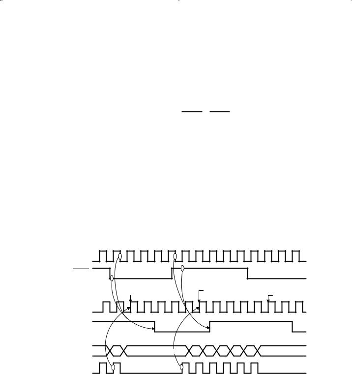
The output-clock-selection register is used to program the desired divided-down frequencies for the reference/shift and video clocks.
2.3.2Frame-Buffer Clocking: Self-Clocked or Externally Clocked
The TVP3010C and the TVP3010M have two pixel-data latching modes, allowing for flexibility in the frame-buffer interface timing. For the pixel port P(0±31), data is always latched on the rising edge of LCLK. If auxiliary-control register (ACR) bit 3 is set to 1 (default), the internal circuitry is configured for self-clocked mode. In this mode, the RCLK or SCLK output of the palette must be used as the timing reference to present data to the pixel port P(0±31). In self-clocked mode, RCLK can be directly tied back to LCLK or LCLK can be a delayed version of RCLK within the timing requirements of the VIP. The self-clocked mode of frame-buffer latching is similar to the operation of the TLC3407X video-interface palette devices.
The VIP internal Blank signal is generated from either VGABL or SYSBL, depending on whether the VGA port is enabled (multiplexer control register 2 (MCR2) bit 7 = 1) or disabled (MCR2 bit 7 = 0). The rising edge of CLK0 latches VGABL when the VGA port is enabled. The falling edge of VCLK is used to sample and latch the SYSBL input when the VGA port is disabled. When the internal Blank signal becomes active, SCLK is disabled as soon as possible. For example, if SCLK is high when the sampled SYSBL goes low, SCLK is allowed to complete the clock cycle and return to the low state. SCLK then is held low until the sampled SYSBL signal goes back high. At this time, SCLK is enabled to clock the first pixel data valid from VRAM. The VIP video-blanking circuitry is designed with sufficient pipeline delay to allow the internal sampled SYSBL and VGABL signals to align with the pipelined RGB data to the video DACs. The logic described previously works in situations where the SCLK period is shorter than, equal to, or longer than the VCLK period.
When in the self-clocked mode, the SCLK control timing is designed to interface directly with the external VRAM. The shift register in the system VRAM is supposed to be updated during the blank active period. When the SYSBL input is sampled high by the falling edge of VCLK, the VRAM shift clock (SCLK) is restarted to clock the VRAM and enable the first group of pixel data to appear on the pixel bus as well as at the TVP3010 pixel input port. The second SCLK causes the VRAM shift register to shift out the second group of data. At the same time, LCLK latches the first group of pixel data into the VIP (see Figure 2±2 for a detailed timing-diagram).
VCLK
In Phase
SYSBL
at Input Terminal
Latch Last Group
of Pixel Data
LD
Internal Delayed
LCLK = RCLK
Blank (internal signal before dot-clock pipeline delay)
Latch First Group of Pixel Data Latch Last Group of Pixel Data
1st |
2nd |
3rd |
4th |
5th |
Group Group |
Group Group Group |
|||
Pixel Data |
Last Group of Pixel Data |
6th |
|
at Input Terminal |
Group |
||
|
SCLK
Figure 2±2. SCLK / VCLK Control Timing
(SSRT Disabled, RCLK / SCLK Frequency = VCLK Frequency)
The RCLK/SCLK phase relationship is designed so that timing specifications are satisfied for the case where SCLK is driving a typical 2-MB VRAM load and RCLK is connected to LCLK. If an external buffer is
2±8

required on SCLK so that it can drive a larger load, a similar buffer can be placed on RCLK to match the signal delay before connecting to LCLK. However, the delay from LCLK to RCLK cannot exceed one RCLK period ±7 ns, (see the timing-parameter specifications for more details).
When the VRAM split shift register operation is performed (see Figure 2±3 and Figure 2±4), the SCLK timing is adjusted to work with the SFLAG input. Basically, the split shift register operation inserts an SCLK during the blank period. This causes the first group of pixel data to appear at the pixel port during blank and allows the first group of data to be displayed as soon as the palette comes out of blank. Figures 2±3 and 2±5 show the case when the SSRT (split shift register transfer) function is enabled. When a rising edge occurs on the SFLAG input, one SCLK with a minimum 15-ns pulse duration is generated after the specified delay. Since this is designed to meet VRAM timing requirements, the SSRT-generated SCLK replaces the first SCLK in the regular shift register transfer case as described above (see Section 2.15 for a detailed explanation of the SSRT function).
VCLK
In Phase
SYSBL
at Input Terminal
SFLAG Input |
|
|
|
|
|
|
|
|
Latch Last Group |
|
Latch First Group of Pixel Data Latch Last Group |
||||
|
of Pixel Data |
|
|||||
LD |
|
|
|
|
|
|
of Pixel Data |
Internal Delayed |
|
|
|
|
|
|
|
LCLK = RCLK |
|
|
|
|
|
|
|
Blank |
|
|
|
|
|
|
|
(internal signal |
|
|
|
|
|
|
|
before dot-clock |
|
|
|
|
|
|
|
pipeline delay) |
|
|
|
|
|
|
|
Pixel Data |
Last |
1st Group of |
2nd |
3rd |
4th |
5th |
6th |
at Input Terminal |
Group |
Pixel Data |
Group |
Group |
Group |
Group |
Group |
SCLK Between Split Shift-Register and Regular Shift-Register Transfer
SCLK
Figure 2±3. SCLK/VCLK Control Timing
(SSRT Enabled, RCLK/SCLK Frequency = VCLK Frequency)
2±9

VCLK
In Phase
SYSBL
at Input Terminal
Latch Last Group
of Pixel Data
LD
Internal Delayed LCLK = RCLK
 Latch first Group of Pixel Data
Blank (internal signal before dot-clock pipeline delay)
Pixel Data |
Last Group of Pixel Data |
1st |
2nd |
3rd |
4th |
5th |
6th |
7th |
|
at Input Terminal |
Group |
Group |
Group |
Group |
Group |
Group |
Group |
||
|
SCLK
Figure 2±4. SCLK/VCLK Control Timing
(SSRT Disabled, RCLK/SCLK Frequency = 4 x VCLK Frequency)
VCLK
In Phase
SYSBL
at Input Terminal
SFLAG Input
|
Latch Last Group |
Latch Second Group |
LD |
of Pixel Data |
of Pixel Data |
|
|
|
Internal Delayed |
|
|
LCLK = RCLK |
|
|
Blank |
|
Latch First Group of Pixel Data |
|
|
|
(internal signal |
|
|
before dot-clock |
|
|
pipeline delay) |
|
|
Pixel Data
at Input Terminal
SCLK
Last |
First Group of Pixel Data |
2nd |
3rd |
4th |
5th |
6th |
7th |
|
Group |
Group |
Group |
Group |
Group |
Group |
Group |
||
|
SCLK Between Split Shift-Register Transfer and Regular Shift-Register Transfer
Figure 2±5. SCLK/VCLK Control Timing
(SSRT Enabled, RCLK/SCLK Frequency = 4 x VCLK Frequency)
2±10

Externally clocked timing can be chosen for the pixel bus P(10±31) by clearing auxiliary control register bit 3 to 0. In externally clocked mode, the RCLK or SCLK output of the palette is not used as the timing reference to present data to the pixel bus. Instead, pixel data is presented to the palette with a synchronous clock and all palette timing is referenced to this clock. In this mode, the external clock should be connected to LCLK and the selected clock input. (When the VGA port is enabled, the CLK0 input is selected independent of the input-clock selection register.)
The externally clocked frame-buffer interface mode is intended for applications where windowed or pixel-by-pixel switching between the VGA port and the pixel port is desired in non-VRAM-based graphics systems. In such applications, the VGA port is enabled (multiplexer control register bit 7 set to 1) and the appropriate direct-color mode is set in the multiplexer control register. The auxiliary-window, port-select, and/or color-key switching functions are then configured and enabled to perform the desired switching. By setting the frame-buffer interface to the externally clocked mode, the pixel port and VGA port timing and pipeline delay are made the same. Also, since the VGA port is enabled, all video-control signal timing is referenced to CLK0, utilizing the VGABL, HSYNC, and VSYNC inputs.
The externally clocked frame-buffer interface timing can also be used in non-VGA switching applications, utilizing only the pixel port or only the VGA port. In either case, it is recommended that VGA video-control signals be used (i.e., VGABL, HSYNC, VSYNC). In this way, all pixel data and video-control signals are referenced to CLK0 and video blank and sync are aligned with pixel data.
NOTE:
When the pixel port is used in externally clocked mode (ACR3 = 0), RCLK must be set to VCLK/1 (DOT/1) in the output-clock selection register and a 1:1 multiplexing mode must be selected in the multiplexer control registers (see Table 2±6). The external clock should be connected to the LCLK input as well as the selected clock input. When the VGA port is also enabled (MCRB7 = 1), CLK0 is selected as the input clock independent of the input-clock selection-register setting.
VGA switching can only be performed using a 1:1 multiplexing mode.
Overlay switching can only be performed using a 1:1 multiplexing mode when the pixel port is set for externally clocked mode. When the pixel port is self-clocked, any of the multiplex ratios may be used (see subsection 2.4.6).
When VGA switching is to be performed using externally clocked mode (ACR3 = 0), the full VGA port frequency of 85 MHz may be utilized provided that the VGA port and the pixel port are both synchronized to the CLK0 input clock.
If VGA switching is to be performed using self-clocked mode (ACR3 = 1), the maximum pixel rate cannot exceed 50 MHz. This is because of internal delay from the CLK0 input to the RCLK output. For external clocked timing, the LCLK input needs to be enabled on terminal 73 (TVP3010C) or terminal L3 (TVP3010M) by programming the configuration register bit 5 to 1.
VGA-data pipeline delay is adjusted within each VIP depending on whether selfor externally clocked frame-buffer interface timing is used (see subsection 2.3.2 ). If the VIP is programmed for self-clocked timing, three additional dot-clock pipeline delays are inserted into the internal VGA-data path and into the internal blanking signal. The additional pipeline delay accounts for the difference between VGABL or SYSBL and the pixel-data inputs P(0±31) when used in the selfand externally clocked modes. This is so the VGA and pixel-port data remain synchronous in time when doing auxiliary window, port select, or color-keyed switching (see Section 2.6). When externally clocked timing is used, the VGA port and the pixel port are already synchronous since both data and blanking are presented to the palette during the same CLK0 clock cycle.
2±11
Loading...