


TPS77127DGKR
Texas Instruments TPS77127DGKR, TPS77127DGK, TPS77118DGKR, TPS77118DGK, TPS77101DGKR Datasheet
...
TPS77101, TPS77118, TPS77127, TPS77128, TPS77133 WITH RESET OUTPUT
TPS77201, TPS77218, TPS77227, TPS77228, TPS77233 WITH POWER GOOD OUTPUT
150-mA LDO REGULATORS WITH INTEGRATED RESET OR PG
SLVS225A – FEBRUARY 2000 – REVISED MARCH 2000
1
POST OFFICE BOX 655303 • DALLAS, TEXAS 75265
D
Open Drain Power-On Reset With 220-ms
Delay (TPS771xx)
D
Open Drain Power-Good (PG) Status
Output (TPS772xx)
D
150-mA Low-Dropout Voltage Regulator
D
Available in 1.8-V, 2.7-V, 2.8-V, 3.3-V, Fixed
Output and Adjustable Versions
D
Dropout Voltage Typically 115 mV
at 150 mA (TPS77133, TPS77233)
D
Ultra Low 92-µA Quiescent Current (Typ)
D
8-Pin MSOP (DGK) Package
D
Low Noise (55 µV
rms
) Without External
Filter (Bypass) Capacitor (TPS77118,
TPS77218)
D
2% Tolerance Over Specified Conditions
for Fixed-Output Versions
D
Fast Transient Response
D
Thermal Shutdown Protection
description
The TPS771xx and TPS772xx are low dropout
regulators with integrated power-on reset and
power good (PG) function respectively. These
devices are capable of supplying 150 mA of output
current with a dropout of 115 mV (TPS77133,
TPS77233). Quiescent current is 92 µA at full load
dropping down to 1 µA when device is disabled.
These devices are optimized to be stable with a
wide range of output capacitors including low ESR
ceramic (10 µF) or low capacitance (1 µF)
tantalum capacitors. These devices have ex-
tremely low noise output performance (55 µV
rms
)
without using any added filter capacitors.
TPS771xx and TPS772xx are designed to have
fast transient response for larger load current
changes.
The TPS771xx or TPS772xx is offered in 1.8-V, 2.7-V, 2.8-V and 3.3-V fixed-voltage versions and in an
adjustable version (programmable over the range of 1.5 V to 5.5 V). Output voltage tolerance is 2% over line,
load, and temperature ranges. The TPS771xx and TPS772xx families are available in 8-pin MSOP (DGK)
packages.
Please be aware that an important notice concerning availability, standard warranty, and use in critical applications of
Texas Instruments semiconductor products and disclaimers thereto appears at the end of this data sheet.
This document contains information on products in more than one phase
of development. The status of each device is indicated on the page(s)
specifying its electrical characteristics.
Copyright 2000, Texas Instruments Incorporated
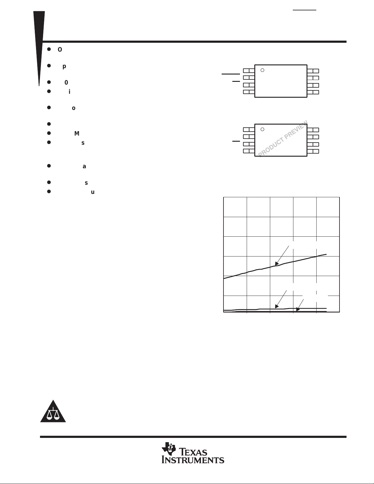
FB/SENSE
PG
EN
GND
OUT
OUT
IN
IN
TPS772xx
DGK PACKAGE
(TOP VIEW)
TPS77x33
DROPOUT VOLTAGE
vs
JUNCTION TEMPERATURE
150
100
50
0
–40 0 40 80
200
250
300
120 140
T
J
– Junction Temperature – °C
– Dropout Voltage – mV
V
DO
I
O
= 150 mA
I
O
= 10 mA
I
O
= 0 A
FB/SENSE
RESET
EN
GND
OUT
OUT
IN
IN
TPS771xx
DGK PACKAGE
(TOP VIEW)
1
2
3
4
8
7
6
5
1
2
3
4
8
7
6
5
TPS77101, TPS77118, TPS77127, TPS77128, TPS77133 WITH RESET OUTPUT
TPS77201, TPS77218, TPS77227, TPS77228, TPS77233 WITH POWER GOOD OUTPUT
150-mA LDO REGULATORS WITH INTEGRATED RESET OR PG
SLVS225A – FEBRUARY 2000 – REVISED MARCH 2000
2
POST OFFICE BOX 655303 • DALLAS, TEXAS 75265
description (continued)
Because the PMOS device behaves as a low-value resistor, the dropout voltage is very low (typically 115 mV
at an output current of 150 mA for 3.3 volt option) and is directly proportional to the output current. Additionally ,
since the PMOS pass element is a voltage-driven device, the quiescent current is very low and independent
of output loading (typically 92 µA over the full range of output current, 0 mA to 150 mA). These two key
specifications yield a significant improvement in operating life for battery-powered systems.
The device is enabled when the EN
pin is connected to a low-level input voltage. This LDO family also features
a sleep mode; applying a TTL high signal to EN (enable) shuts down the regulator, reducing the quiescent
current to less than 1 µA at T
J
= 25°C.
The TPS771xx features an integrated power-on reset, commonly used as a supply voltage supervisor (SVS)
or reset output voltage. The RESET output of the TPS771xx initiates a reset in DSP, microcomputer or
microprocessor systems at power-up and in the event of an undervoltage condition. An internal comparator in
the TPS771xx monitors the output voltage of the regulator to detect an undervoltage condition on the regulated
output voltage. When OUT
reaches 95% of its regulated voltage, RESET will go to a high-impedance state after
a 220 ms delay . RESET will go to low-impedance state when OUT is pulled below 95% (i.e. over load condition)
of its regulated voltage.
For the TPS772xx, the power good terminal (PG) is an active high output, which can be used to implement a
power-on reset or a low-battery indicator. An internal comparator in the TPS772xx monitors the output voltage
of the regulator to detect an undervoltage condition on the regulated output voltage. When OUT falls below 82%
of its regulated voltage, PG will go to a low-impedance state. PG will go to a high-impedance state when OUT
is above 82% of its regulated voltage.
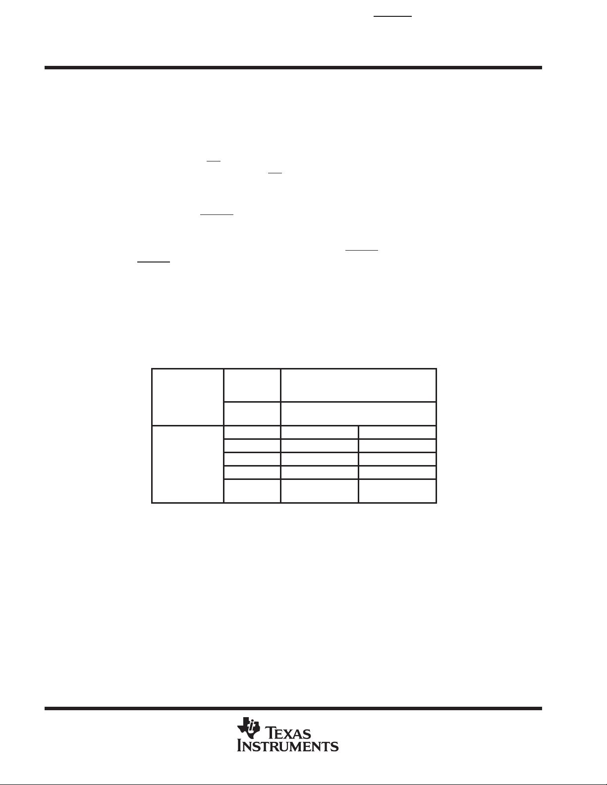
AVAILABLE OPTIONS
T
OUTPUT
VOLTAGE
(V)
PACKAGED DEVICES
J
TYP
MSOP
(DGK)
3.3 TPS77133DGK TPS77233DGK
2.8 TPS77128DGK TPS77228DGK
–
°
°
2.7 TPS77127DGK TPS77227DGK
–40 C
to
125 C
1.8 TPS77118DGK TPS77218DGK
Adjustable
1.5 V to 5.5 V
TPS77101DGK TPS77201DGK
The TPS77101 and TPS77201 are programmable using an external resistor divider
(see application information). The DGK package is available taped and reeled. Add
an R suffix to the device type (e.g., TPS77101DGKR).
TPS77101, TPS77118, TPS77127, TPS77128, TPS77133 WITH RESET OUTPUT
TPS77201, TPS77218, TPS77227, TPS77228, TPS77233 WITH POWER GOOD OUTPUT
150-mA LDO REGULATORS WITH INTEGRATED RESET OR PG
SLVS225A – FEBRUARY 2000 – REVISED MARCH 2000
3
POST OFFICE BOX 655303 • DALLAS, TEXAS 75265
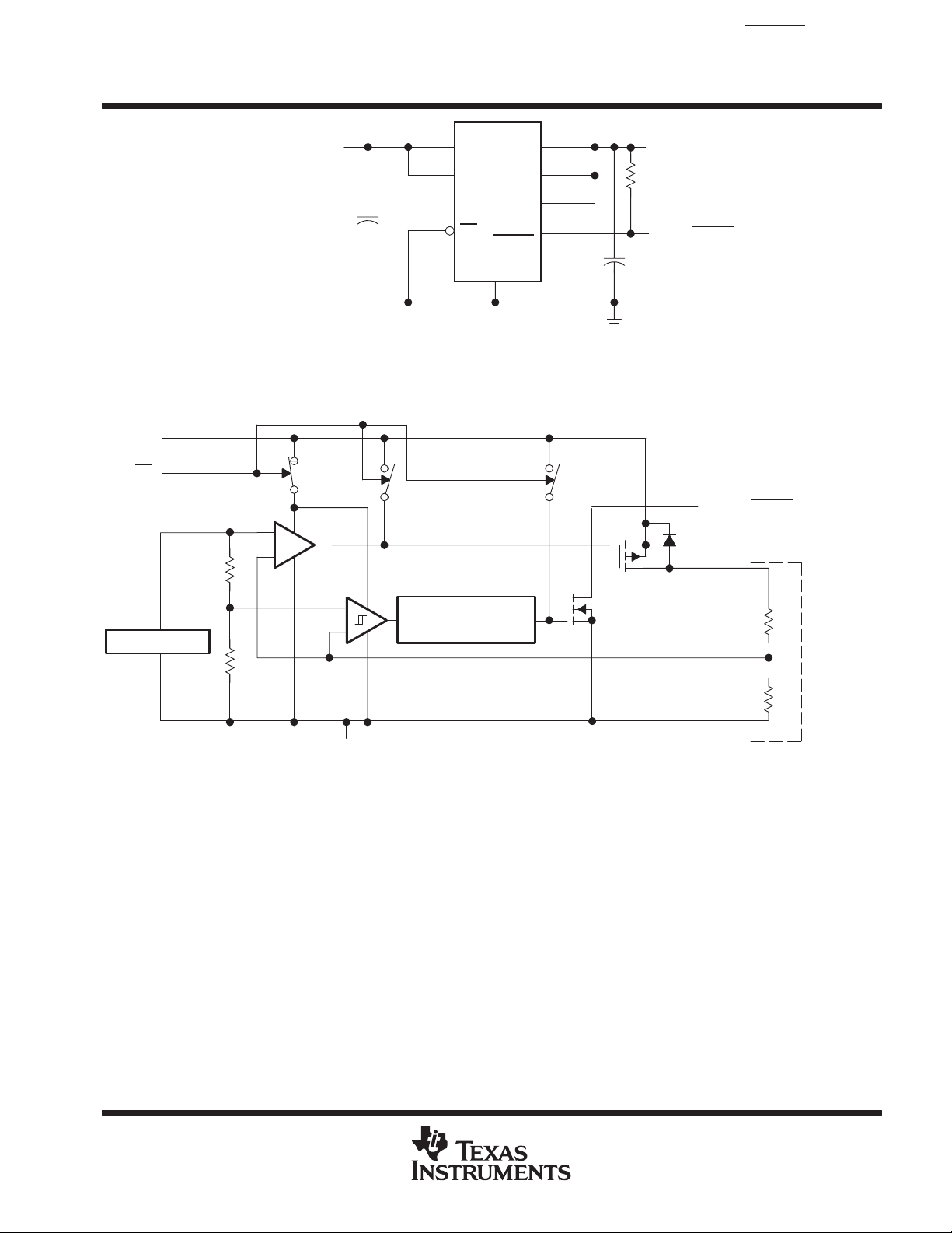
OUT
SENSE
6
5
3
IN
IN
EN
GND
4
7
1
V
I
0.1 µF
10 µF
+
OUT
8
V
O
PG or RESET
PG or
RESET
2
Figure 1. Typical Application Configuration (For Fixed Output Options)
functional block diagram—adjustable version
220 ms Delay
(for TPS771xx Option)
_
+
V
ref
= 1.1834 V
OUT
FB/SENSE
EN
GND
PG or RESET
_
+
IN
External
to
the
device
R1
R2
TPS77101, TPS77118, TPS77127, TPS77128, TPS77133 WITH RESET OUTPUT
TPS77201, TPS77218, TPS77227, TPS77228, TPS77233 WITH POWER GOOD OUTPUT
150-mA LDO REGULATORS WITH INTEGRATED RESET OR PG
SLVS225A – FEBRUARY 2000 – REVISED MARCH 2000
4
POST OFFICE BOX 655303 • DALLAS, TEXAS 75265
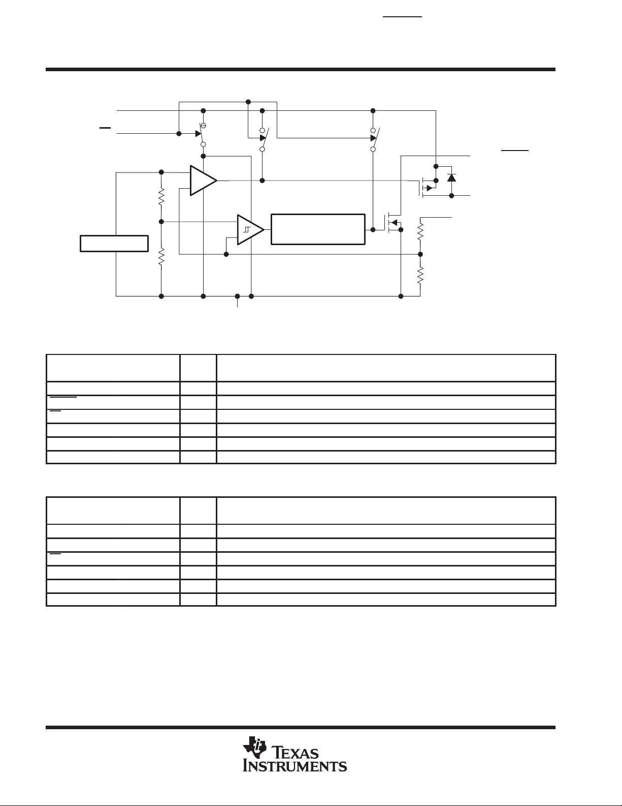
functional block diagram—fixed-voltage version
_
+
V
ref
= 1.1834 V
OUT
EN
GND
R1
R2
PG or RESET
_
+
IN
SENSE
220 ms Delay
(for TPS771xx Option)
Terminal Functions (TPS771xx)
TERMINAL
NAME NO.
I/O
DESCRIPTION
FB/SENSE 1 I Feedback input voltage for adjustable device (sense input for fixed options)
RESET 2 O Reset output
EN 3 I Enable input
GND 4 Regulator ground
IN 5, 6 I Input voltage
OUT 7, 8 O Regulated output voltage
Terminal Functions (TPS772xx)
TERMINAL
NAME NO.
I/O
DESCRIPTION
FB/SENSE 1 I Feedback input voltage for adjustable device (sense input for fixed options)
PG 2 O Power good
EN 3 I Enable input
GND 4 Regulator ground
IN 5, 6 I Input voltage
OUT 7, 8 O Regulated output voltage
TPS77101, TPS77118, TPS77127, TPS77128, TPS77133 WITH RESET OUTPUT
TPS77201, TPS77218, TPS77227, TPS77228, TPS77233 WITH POWER GOOD OUTPUT
150-mA LDO REGULATORS WITH INTEGRATED RESET OR PG
SLVS225A – FEBRUARY 2000 – REVISED MARCH 2000
5
POST OFFICE BOX 655303 • DALLAS, TEXAS 75265
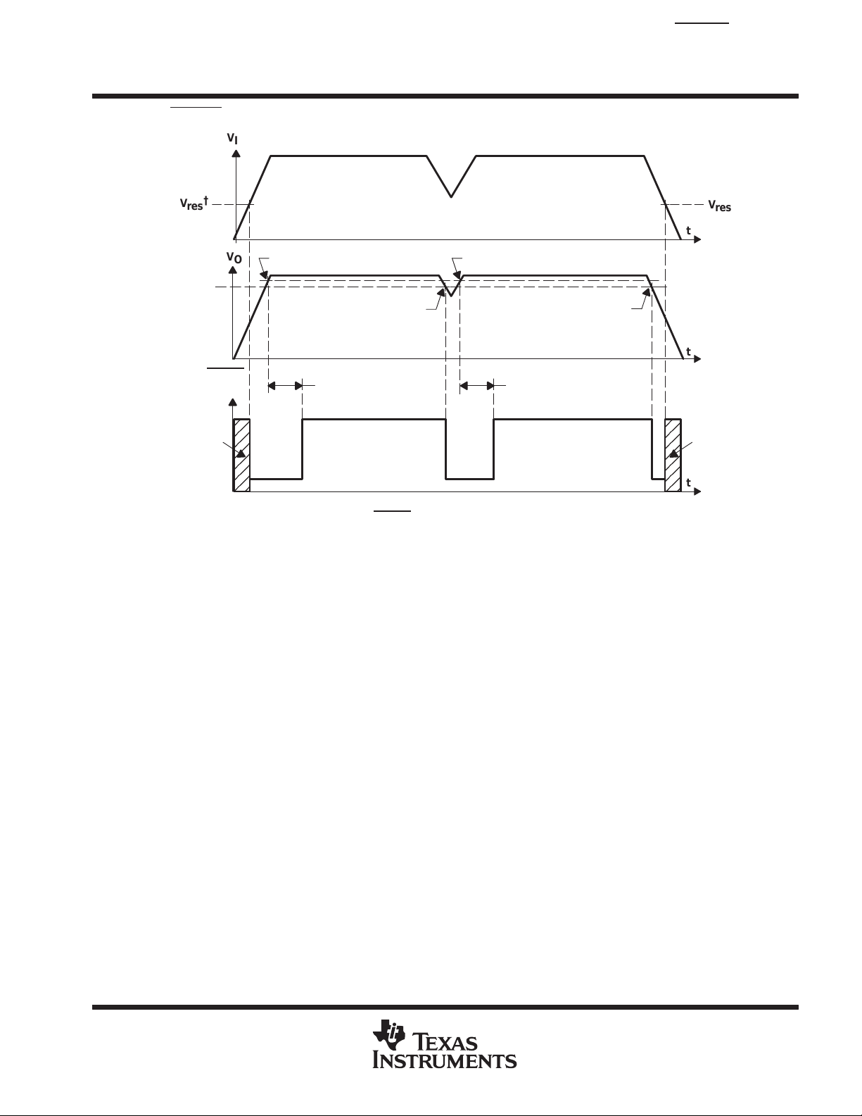
TPS771xx RESET timing diagram
†
V
res
is the minimum input voltage for a valid RESET . The symbol V
res
is not currently listed within EIA or JEDEC standards
for semiconductor symbology.
V
I
V
res
†
V
res
t
t
t
V
O
Threshold
Voltage
RESET
Output
220 ms
Delay
220 ms
Delay
Output
Undefined
Output
Undefined
V
IT+
‡
V
IT–
‡
V
IT–
‡
V
IT+
‡
‡
VIT –Trip voltage is typically 5% lower than the output voltage (95%V
O
) V
IT–
to V
IT+
is the hysteresis voltage.
TPS77101, TPS77118, TPS77127, TPS77128, TPS77133 WITH RESET OUTPUT
TPS77201, TPS77218, TPS77227, TPS77228, TPS77233 WITH POWER GOOD OUTPUT
150-mA LDO REGULATORS WITH INTEGRATED RESET OR PG
SLVS225A – FEBRUARY 2000 – REVISED MARCH 2000
6
POST OFFICE BOX 655303 • DALLAS, TEXAS 75265
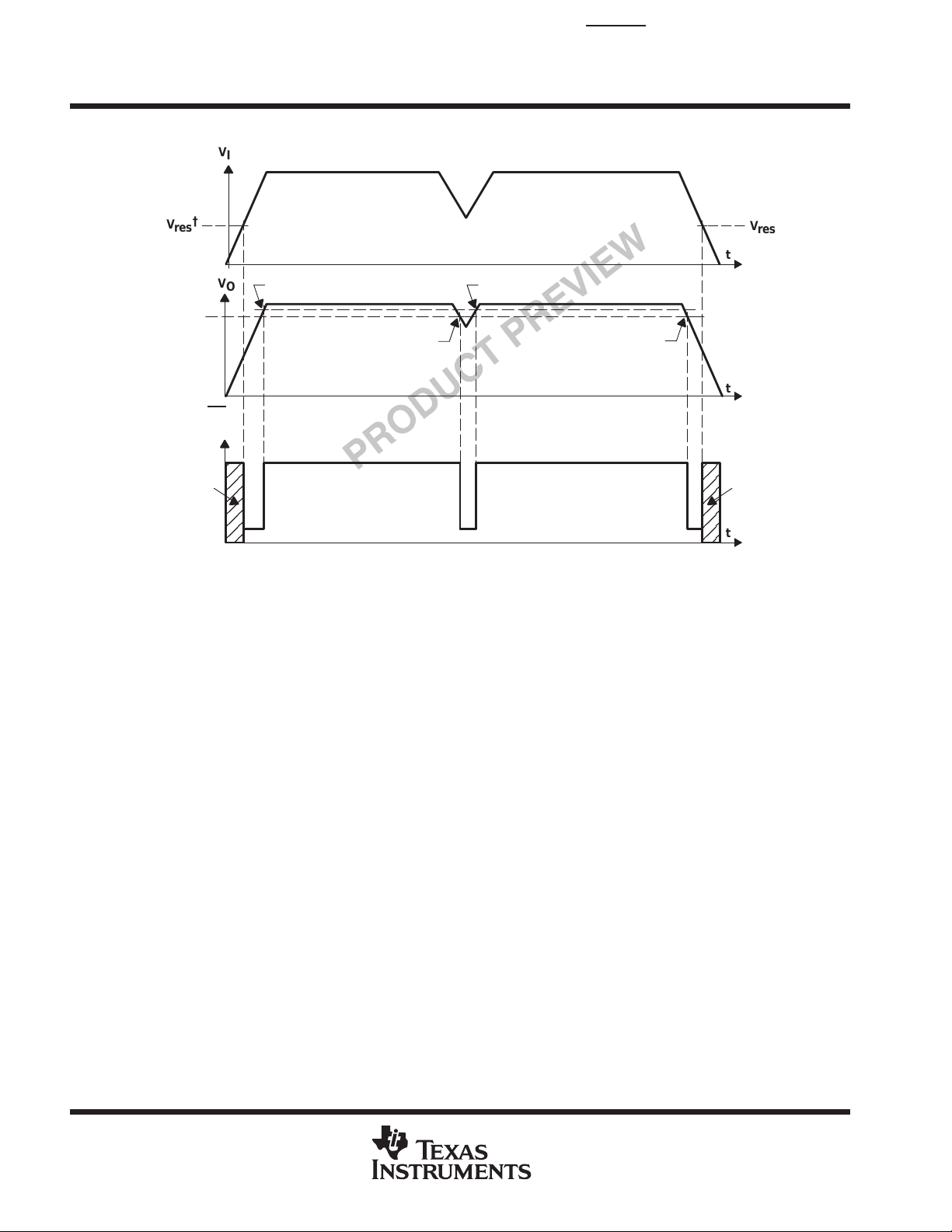
TPS772xx PG timing diagram
†
V
res
is the minimum input voltage for a valid PG. The symbol V
res
is not currently listed within EIA or JEDEC standards for
semiconductor symbology .
V
I
V
res
†
V
res
t
t
t
V
O
Threshold
Voltage
PG
Output
Output
Undefined
Output
Undefined
V
IT+
‡
V
IT–
‡
V
IT–
‡
V
IT+
‡
‡
VIT –Trip voltage is typically 18% lower than the output voltage (82%V
O
) V
IT–
to V
IT+
is the hysteresis voltage.
TPS77101, TPS77118, TPS77127, TPS77128, TPS77133 WITH RESET OUTPUT
TPS77201, TPS77218, TPS77227, TPS77228, TPS77233 WITH POWER GOOD OUTPUT
150-mA LDO REGULATORS WITH INTEGRATED RESET OR PG
SLVS225A – FEBRUARY 2000 – REVISED MARCH 2000
7
POST OFFICE BOX 655303 • DALLAS, TEXAS 75265
absolute maximum ratings over operating junction temperature range
(unless otherwise noted)
Ĕ
Input voltage range
‡
, V
I
–0.3 V to 13.5 V. . . . . . . . . . . . . . . . . . . . . . . . . . . . . . . . . . . . . . . . . . . . . . . . . . . . . . . . . .
Voltage range at EN –0.3 V to 16.5 V. . . . . . . . . . . . . . . . . . . . . . . . . . . . . . . . . . . . . . . . . . . . . . . . . . . . . . . . . . . . . .
Maximum RESET voltage (TPS771xx) 16.5 V. . . . . . . . . . . . . . . . . . . . . . . . . . . . . . . . . . . . . . . . . . . . . . . . . . . . . .
Maximum PG voltage (TPS772xx) 16.5 V. . . . . . . . . . . . . . . . . . . . . . . . . . . . . . . . . . . . . . . . . . . . . . . . . . . . . . . . .
Peak output current Internally limited. . . . . . . . . . . . . . . . . . . . . . . . . . . . . . . . . . . . . . . . . . . . . . . . . . . . . . . . . . . . . .
Continuous total power dissipation See dissipation rating tables. . . . . . . . . . . . . . . . . . . . . . . . . . . . . . . . . . . . . .
Output voltage, V
O
(OUT, FB) 5.5 V. . . . . . . . . . . . . . . . . . . . . . . . . . . . . . . . . . . . . . . . . . . . . . . . . . . . . . . . . . . . . .
Operating virtual junction temperature range, T
J
–40°C to 125°C. . . . . . . . . . . . . . . . . . . . . . . . . . . . . . . . . . . . .
Storage temperature range, T
stg
–65°C to 150°C. . . . . . . . . . . . . . . . . . . . . . . . . . . . . . . . . . . . . . . . . . . . . . . . . . .
ESD rating, HBM 2 kV. . . . . . . . . . . . . . . . . . . . . . . . . . . . . . . . . . . . . . . . . . . . . . . . . . . . . . . . . . . . . . . . . . . . . . . . . .
†
Stresses beyond those listed under “absolute maximum ratings” may cause permanent damage to the device. These are stress ratings only, and
functional operation of the device at these or any other conditions beyond those indicated under “recommended operating conditions” is not
implied. Exposure to absolute-maximum-rated conditions for extended periods may affect device reliability.
‡
All voltage values are with respect to network terminal ground.
DISSIPATION RATING TABLE – FREE-AIR TEMPERATURES
PACKAGE
AIR FLOW
(CFM)
θ
JA
(°C/W)
θ
JC
(°C/W)
T
A
< 25°C
POWER RATING
DERATING FACTOR
ABOVE T
A
= 25°C
T
A
= 70°C
POWER RATING
T
A
= 85°C
POWER RATING
0 266.2 3.84 376 mW 3.76 mW/°C 207 mW 150 mW
DGK
150 255.2 3.92 392 mW 3.92 mW/°C 216 mW 157 mW
250 242.8 4.21 412 mW 4.12 mW/°C 227 mW 165 mW
recommended operating conditions
MIN MAX UNIT
Input voltage, V
I
§
2.7 10 V
Output voltage range, V
O
1.5 5.5 V
Output current, I
O
(see Note 1) 0 150 mA
Operating virtual junction temperature, T
J
(see Note 1) –40 125 °C
§
To calculate the minimum input voltage for your maximum output current, use the following equation: V
I(min)
= V
O(max)
+ V
DO(max
load)
.
NOTE 1: Continuous current and operating junction temperature are limited by internal protection circuitry, but it is not recommended that the
device operate under conditions beyond those specified in this table for extended periods of time.
 Loading...