


Texas Instruments CD74ACT153M96, CD74ACT153M, CD74ACT153E, CD74AC153M96, CD74AC153E Datasheet
...
Data sheet acquired from Harris Semiconductor SCHS237
September 1998
CD74AC153,
CD74ACT153
Dual 4-Input Multiplexer
Features |
Description |
||||||
• |
Buffered Inputs |
The CD74AC153 and CD74ACT153 are dual 4-input multi- |
|||||
• |
Typical Propagation Delay |
plexers that utilize the Harris Advanced CMOS Logic tech- |
|||||
nology. One of the four sources for each section is selected |
|||||||
|
- 6.3ns at VCC = 5V, TA = 25oC, CL = 50pF |
||||||
|
by the common Select inputs, S0 and S1. When the Enable |
||||||
• |
Exceeds 2kV ESD Protection MIL-STD-883, Method |
inputs |
(1E, |
|
2E) |
are HIGH, the outputs are in the low state. |
|
|
|
|
|
|
|||
|
3015 |
Ordering Information |
|||||
|
|
||||||
|
• |
SCR-Latchup-Resistant CMOS Process and Circuit |
|
|
|
|
|||
[ /Title |
|
Design |
|
PART |
TEMP. |
PACKAGE |
PKG. |
||
|
|
|
|
NUMBER |
RANGE (oC) |
NO. |
|||
(CD74 |
• Speed of Bipolar FAST™/AS/S with Significantly |
|
CD74AC153E |
0 to 70oC, -40 to 85, |
16 Ld PDIP |
E16.3 |
|||
AC153 |
|
Reduced Power Consumption |
|
|
|
-55 to 125 |
|
|
|
|
|
|
|
|
|
|
|
||
, |
• |
Balanced Propagation Delays |
|
CD74ACT153E |
0 to 70oC, -40 to 85, |
16 Ld PDIP |
E16.3 |
||
CD74 |
• AC Types Feature 1.5V to 5.5V Operation and |
|
|
|
-55 to 125 |
|
|
||
|
|
|
0 to 70oC, -40 to 85, |
|
|
||||
ACT15 |
|
Balanced Noise Immunity at 30% of the Supply |
|
CD74AC153M96 |
16 Ld SOIC |
M16.15 |
|||
3) |
• ±24mA Output Drive Current |
|
|
|
-55 to 125 |
|
|
||
|
CD74ACT153M |
0 to 70oC, -40 to 85, |
16 Ld SOIC |
M16.15 |
|||||
/Sub- |
|
- |
Fanout to 15 FAST™ ICs |
|
|||||
|
|
|
|
-55 to 125 |
|
|
|||
ject |
|
- |
Drives 50Ω Transmission Lines |
|
|
|
|
|
|
|
|
NOTES: |
|
|
|
|
|||
(Dual |
|
|
|
|
|
|
|
|
|
|
|
|
|
1. When ordering, use the entire part number. Add the suffix 96 to |
|||||
4-Input |
|
|
|
|
|||||
|
|
|
|
obtain the variant in the tape and reel. |
|
|
|||
Multi- |
|
|
|
|
2. Wafer and die for this part number is available which meets all elec- |
||||
plexer) |
|
|
|
|
trical specifications. Please contact your local sales office or Harris |
||||
|
|
|
|
customer service for ordering information. |
|
||||
/Autho |
|
|
|
|
|
||||
|
|
|
|
|
|
|
|
|
|
r () |
|
|
|
|
|
|
|
|
|
/Key- |
Pinout |
|
|
|
|
|
|
||
words |
|
|
|
|
|
|
|||
|
|
CD74AC153, CD74ACT153 |
|
|
|
||||
(Har- |
|
|
|
|
|
||||
|
|
|
|
(PDIP, SOIC) |
|
|
|
|
|
ris |
|
|
|
|
|
|
|
|
|
|
|
|
|
TOP VIEW |
|
|
|
|
|
Semi- |
|
|
|
|
|
|
|
|
|
con- |
|
|
1E |
1 |
16 VCC |
|
|
|
|
ductor, |
|
|
|
|
|
||||
|
|
S1 |
2 |
15 |
2E |
|
|
|
|
Advan |
|
|
|
|
|
||||
|
|
1I3 |
3 |
14 |
S0 |
|
|
|
|
ced |
|
|
|
|
|
||||
|
|
1I2 |
4 |
13 |
2I3 |
|
|
|
|
CMOS |
|
|
|
|
|
||||
|
|
1I1 |
5 |
12 |
2I2 |
|
|
|
|
) |
|
|
|
|
|
||||
|
|
1I0 |
6 |
11 |
2I1 |
|
|
|
|
/Cre- |
|
|
|
|
|
||||
|
|
1Y |
7 |
10 |
2I0 |
|
|
|
|
ator () |
|
|
|
|
|
||||
|
|
GND |
8 |
9 |
2Y |
|
|
|
|
/DOCI |
|
|
|
|
|
||||
|
|
|
|
|
|
|
|
|
|
NFO |
|
|
|
|
|
|
|
|
|
pdf- |
|
|
|
|
|
|
|
|
|
mark |
|
|
|
|
|
|
|
|
|
CAUTION: These devices are sensitive to electrostatic discharge. Users should follow proper IC Handling Procedures.
File Number 1966.1
FAST™ is a Trademark of Fairchild Semiconductor. |
1 |
|
Copyright © Harris Corporation 1998 |
||
|
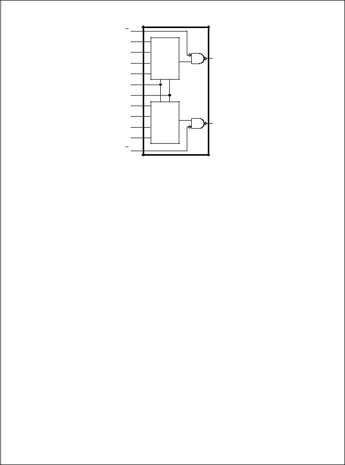
CD74AC153, CD74ACT153
Functional Diagram
1 |
|
|
1E |
|
|
6 |
|
|
1I0 |
|
|
5 |
|
|
1I1 |
SEL/MUX |
7 1Y |
4 |
||
1I2 |
|
|
3 |
|
|
1I3 |
|
|
14 |
|
|
S0 |
|
|
2 |
|
|
S1 |
|
|
10 |
|
|
2I0 |
|
|
11 |
|
|
2I1 |
SEL/MUX |
9 2Y |
12 |
||
2I2 |
|
|
13 |
|
|
2I3 |
|
|
15 |
|
|
2E |
|
|
|
|
GND = 8 |
|
|
VCC = 16 |
TRUTH TABLE
|
|
|
|
|
|
ENABLE |
|
||
SELECT INPUTS |
|
DATA INPUTS |
|
INPUTS |
OUTPUT |
||||
|
|
|
|
|
|
|
|
|
|
S1 |
S0 |
nI0 |
nI1 |
nI2 |
nI3 |
|
|
|
nY |
|
nE |
||||||||
X |
X |
X |
X |
X |
X |
|
H |
L |
|
|
|
|
|
|
|
|
|
|
|
L |
L |
L |
X |
X |
X |
|
L |
L |
|
|
|
|
|
|
|
|
|
|
|
L |
L |
H |
X |
X |
X |
|
L |
H |
|
|
|
|
|
|
|
|
|
|
|
L |
H |
X |
L |
X |
X |
|
L |
L |
|
|
|
|
|
|
|
|
|
|
|
L |
H |
X |
H |
X |
X |
|
L |
H |
|
|
|
|
|
|
|
|
|
|
|
H |
L |
X |
X |
L |
X |
|
L |
L |
|
|
|
|
|
|
|
|
|
|
|
H |
L |
X |
X |
H |
X |
|
L |
H |
|
|
|
|
|
|
|
|
|
|
|
H |
H |
X |
X |
X |
L |
|
L |
L |
|
|
|
|
|
|
|
|
|
|
|
H |
H |
X |
X |
X |
H |
|
L |
H |
|
|
|
|
|
|
|
|
|
|
|
Select inputs S1 and S0 are common to both sections. H = High Level, L = Low Level, X = Don’t Care, Z = High Impedance.
2

CD74AC153, CD74ACT153
Absolute Maximum Ratings
DC Supply Voltage, VCC . . . . . . . . . . . . . . . . . . . . . . . . |
-0.5V to 6V |
DC Input Diode Current, IIK |
±20mA |
For VI < -0.5V or VI > VCC + 0.5V . . . . . . . . . . . . . . . . . . |
|
DC Output Diode Current, IOK |
±50mA |
For VO < -0.5V or VO > VCC + 0.5V . . . . . . . . . . . . . . . . |
|
DC Output Source or Sink Current per Output Pin, IO |
±50mA |
For VO > -0.5V or VO < VCC + 0.5V . . . . . . . . . . . . . . . . |
|
DC VCC or Ground Current, ICC or IGND (Note 3) . . . . . . |
. . .±100mA |
Thermal Information |
|
Thermal Resistance (Typical, Note 5) |
θJA (oC/W) |
PDIP Package . . . . . . . . . . . . . . . . . . . . . . . . . . . . |
. 90 |
SOIC Package . . . . . . . . . . . . . . . . . . . . . . . . . . . . |
. 160 |
Maximum Junction Temperature (Plastic Package) . . . |
. . . . . . . 150oC |
Maximum Storage Temperature Range . . . . . . . . . . |
-65oC to 150oC |
Maximum Lead Temperature (Soldering 10s) . . . . . . |
. . . . . . . 300oC |
Operating Conditions
Temperature Range, TA . . . . . . . . . . . . . . . . . . . . . . -55oC to 125oC
Supply Voltage Range, VCC (Note 4)
AC Types. . . . . . . . . . . . . . . . . . . . . . . . . . . . . . . . . . .1.5V to 5.5V
ACT Types . . . . . . . . . . . . . . . . . . . . . . . . . . . . . . . . .4.5V to 5.5V
DC Input or Output Voltage, VI, VO . . . . . . . . . . . . . . . . . 0V to VCC
Input Rise and Fall Slew Rate, dt/dv
AC Types, 1.5V to 3V . . . . . . . . . . . . . . . . . . . . . . . . . 50ns (Max)
AC Types, 3.6V to 5.5V . . . . . . . . . . . . . . . . . . . . . . . . 20ns (Max)
ACT Types, 4.5V to 5.5V. . . . . . . . . . . . . . . . . . . . . . . 10ns (Max)
CAUTION: Stresses above those listed in “Absolute Maximum Ratings” may cause permanent damage to the device. This is a stress only rating and operation of the device at these or any other conditions above those indicated in the operational sections of this specification is not implied.
NOTES:
3.For up to 4 outputs per device, add ±25mA for each additional output.
4.Unless otherwise specified, all voltages are referenced to ground.
5.θJA is measured with the component mounted on an evaluation PC board in free air.
DC Electrical Specifications
|
|
TEST |
|
|
|
-40oC TO |
-55oC TO |
|
|||
|
|
CONDITIONS |
VCC |
25oC |
85oC |
125oC |
|
||||
PARAMETER |
SYMBOL |
VI (V) |
IO (mA) |
(V) |
MIN |
MAX |
MIN |
MAX |
MIN |
MAX |
UNITS |
AC TYPES |
|
|
|
|
|
|
|
|
|
|
|
|
|
|
|
|
|
|
|
|
|
|
|
High Level Input Voltage |
VIH |
- |
- |
1.5 |
1.2 |
- |
1.2 |
- |
1.2 |
- |
V |
|
|
|
|
3 |
2.1 |
- |
2.1 |
- |
2.1 |
- |
V |
|
|
|
|
|
|
|
|
|
|
|
|
|
|
|
|
5.5 |
3.85 |
- |
3.85 |
- |
3.85 |
- |
V |
|
|
|
|
|
|
|
|
|
|
|
|
Low Level Input Voltage |
VIL |
- |
- |
1.5 |
- |
0.3 |
- |
0.3 |
- |
0.3 |
V |
|
|
|
|
3 |
- |
0.9 |
- |
0.9 |
- |
0.9 |
V |
|
|
|
|
|
|
|
|
|
|
|
|
|
|
|
|
5.5 |
- |
1.65 |
- |
1.65 |
- |
1.65 |
V |
|
|
|
|
|
|
|
|
|
|
|
|
High Level Output Voltage |
VOH |
VIH or VIL |
-0.05 |
1.5 |
1.4 |
- |
1.4 |
- |
1.4 |
- |
V |
|
|
|
-0.05 |
3 |
2.9 |
- |
2.9 |
- |
2.9 |
- |
V |
|
|
|
|
|
|
|
|
|
|
|
|
|
|
|
-0.05 |
4.5 |
4.4 |
- |
4.4 |
- |
4.4 |
- |
V |
|
|
|
|
|
|
|
|
|
|
|
|
|
|
|
-4 |
3 |
2.58 |
- |
2.48 |
- |
2.4 |
- |
V |
|
|
|
|
|
|
|
|
|
|
|
|
|
|
|
-24 |
4.5 |
3.94 |
- |
3.8 |
- |
3.7 |
- |
V |
|
|
|
|
|
|
|
|
|
|
|
|
|
|
|
-75 |
5.5 |
- |
- |
3.85 |
- |
- |
- |
V |
|
|
|
(Note 6, 7) |
|
|
|
|
|
|
|
|
|
|
|
|
|
|
|
|
|
|
|
|
|
|
|
-50 |
5.5 |
- |
- |
- |
- |
3.85 |
- |
V |
|
|
|
(Note 6, 7) |
|
|
|
|
|
|
|
|
|
|
|
|
|
|
|
|
|
|
|
|
3
 Loading...