


Texas Instruments SN74ABTH162245DGGR, SN74ABTH162245DGVR, SN74ABTH162245DL, SN74ABTH162245DLR Datasheet
|
SN54ABTH162245, SN74ABTH162245 |
||||||||
|
16-BIT BUS TRANSCEIVERS |
||||||||
|
|
|
WITH 3-STATE OUTPUTS |
||||||
|
SCBS712A ± FEBRUARY 1998 ± REVISED APRIL 1999 |
||||||||
|
|
|
|
|
|
|
|
|
|
D Members of the Texas Instruments |
SN54ABTH162245 . . . WD PACKAGE |
||||||||
Widebus Family |
SN74ABTH162245 . . . DGG, DGV, OR DL PACKAGE |
||||||||
D A-Port Outputs Have Equivalent 25-Ω |
|
(TOP VIEW) |
|
|
|
|
|
||
|
|
|
|
|
|
|
|
|
|
Series Resistors, So No External Resistors |
1DIR |
|
|
|
|
|
|
|
|
|
1 |
48 |
|
1OE |
|||||
Are Required |
|
|
|||||||
1B1 |
|
2 |
47 |
|
1A1 |
||||
|
|
||||||||
D State-of-the-Art EPIC-ΙΙB BiCMOS Design |
|
|
|||||||
1B2 |
|
3 |
46 |
|
1A2 |
||||
|
|
||||||||
Significantly Reduces Power Dissipation |
|
|
|||||||
GND |
|
4 |
45 |
|
GND |
||||
|
|
||||||||
D Typical VOLP (Output Ground Bounce) |
|
|
|||||||
1B3 |
|
5 |
44 |
|
1A3 |
||||
|
|
||||||||
< 1 V at VCC = 5 V, TA = 25°C |
1B4 |
|
6 |
43 |
|
1A4 |
|||
|
|
||||||||
D Distributed VCC and GND Pin Configuration |
VCC |
|
7 |
42 |
|
VCC |
|||
|
|
||||||||
|
|
||||||||
Minimizes High-Speed Switching Noise |
1B5 |
|
8 |
41 |
|
1A5 |
|||
D Flow-Through Architecture Optimizes PCB |
1B6 |
|
9 |
40 |
|
1A6 |
|||
|
|
||||||||
|
|
||||||||
Layout |
GND |
|
10 |
39 |
|
GND |
|||
|
|
||||||||
D Bus Hold on Data Inputs Eliminates the |
1B7 |
|
11 |
38 |
|
1A7 |
|||
1B8 |
|
12 |
37 |
|
1A8 |
||||
|
|
||||||||
Need for External Pullup/Pulldown |
|
|
|||||||
2B1 |
|
13 |
36 |
|
2A1 |
||||
|
|
||||||||
Resistors |
|
|
|||||||
2B2 |
|
14 |
35 |
|
2A2 |
||||
D Latch-Up Performance Exceeds 500 mA Per |
|
|
|||||||
GND |
|
15 |
34 |
|
GND |
||||
|
|
||||||||
JESD 17 |
|
|
|||||||
2B3 |
|
16 |
33 |
|
2A3 |
||||
|
|
||||||||
D ESD Protection Exceeds 2000 V Per |
|
|
|||||||
2B4 |
|
17 |
32 |
|
2A4 |
||||
|
|
||||||||
MIL-STD-833, Method 3015; Exceeds 200 V |
VCC |
|
18 |
31 |
|
VCC |
|||
|
|
||||||||
Using Machine Model (C = 200 pF, R = 0) |
|
|
|||||||
2B5 |
|
19 |
30 |
|
2A5 |
||||
D Package Options Include Plastic Thin |
|
|
|||||||
2B6 |
|
20 |
29 |
|
2A6 |
||||
|
|
||||||||
Shrink Small-Outline (DGG), Thin Very |
GND |
|
21 |
28 |
|
GND |
|||
|
|
||||||||
Small-Outline (DGV), and Shrink |
2B7 |
|
22 |
27 |
|
2A7 |
|||
|
|
||||||||
Small-Outline (DL) Packages and 380-mil |
2B8 |
|
23 |
26 |
|
2A8 |
|||
|
|
||||||||
Fine-Pitch Ceramic Flat (WD) Package |
2DIR |
|
24 |
25 |
|
|
|
|
|
|
|
2OE |
|
||||||
Using 25-mil Center-to-Center Spacings |
|
|
|
|
|
|
|
|
|
|
|
|
|
|
|
|
|
|
|
description
The 'ABTH162245 devices are 16-bit noninverting 3-state transceivers designed for synchronous two-way communication between data buses. The control-function implementation minimizes external timing requirements.
These devices can be used as two 8-bit transceivers or one 16-bit transceiver. They allow data transmission from the A bus to the B bus or from the B bus to the A bus, depending on the logic level at the direction-control (DIR) input. The output-enable (OE) input can be used to disable the device so that the buses are effectively isolated.
The A-port outputs, which are designed to source or sink up to 12 mA, include equivalent 25-Ω series resistors to reduce overshoot and undershoot.
Active bus-hold circuitry is provided to hold unused or floating data inputs at a valid logic level.
To ensure the high-impedance state during power up or power down, OE should be tied to VCC through a pullup resistor; the minimum value of the resistor is determined by the current-sinking capability of the driver.
The SN54ABTH162245 is characterized for operation over the full military temperature range of ±55°C to 125°C. The SN74ABTH162245 is characterized for operation from ±40°C to 85°C.
Please be aware that an important notice concerning availability, standard warranty, and use in critical applications of Texas Instruments semiconductor products and disclaimers thereto appears at the end of this data sheet.
Widebus and EPIC-ΙΙB are trademarks of Texas Instruments Incorporated.
UNLESS OTHERWISE NOTED this document contains PRODUCTION DATA information current as of publication date. Products conform to specifications per the terms of Texas Instruments standard warranty. Production processing does not necessarily include testing of all parameters.
Copyright 1999, Texas Instruments Incorporated
POST OFFICE BOX 655303 •DALLAS, TEXAS 75265 |
1 |

SN54ABTH162245, SN74ABTH162245 16-BIT BUS TRANSCEIVERS
WITH 3-STATE OUTPUTS
SCBS712A ± FEBRUARY 1998 ± REVISED APRIL 1999
FUNCTION TABLE (each 8-bit section)
|
INPUTS |
OPERATION |
|
|
|
|
|
|
|
DIR |
|
|
OE |
||
|
|
||
|
L |
L |
B data to A bus |
|
L |
H |
A data to B bus |
|
H |
X |
Isolation |
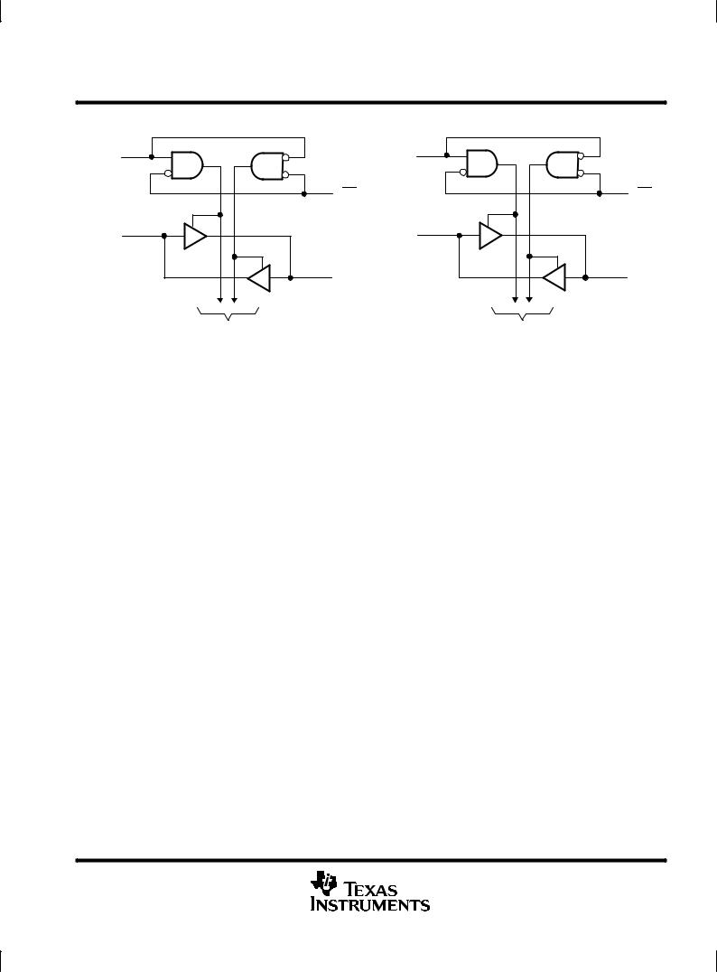
logic symbol²
48 |
G3 |
|
1OE |
|
|
1 |
3 EN1 [BA] |
|
1DIR |
|
|
25 |
3 EN2 [AB] |
|
G6 |
|
|
2OE |
|
|
24 |
6 EN4 [BA] |
|
2DIR |
|
|
|
6 EN5 [AB] |
|
47 |
1 |
2 |
1A1 |
1B1 |
|
46 |
|
2 |
|
3 |
|
1A2 |
|
1B2 |
44 |
|
5 |
1A3 |
|
1B3 |
43 |
|
6 |
1A4 |
|
1B4 |
41 |
|
8 |
1A5 |
|
1B5 |
40 |
|
9 |
1A6 |
|
1B6 |
38 |
|
11 |
1A7 |
|
1B7 |
37 |
|
12 |
1A8 |
|
1B8 |
36 |
4 |
13 |
2A1 |
2B1 |
|
35 |
|
5 |
|
14 |
|
2A2 |
|
2B2 |
33 |
|
16 |
2A3 |
|
2B3 |
32 |
|
17 |
2A4 |
|
2B4 |
30 |
|
19 |
2A5 |
|
2B5 |
29 |
|
20 |
2A6 |
|
2B6 |
27 |
|
22 |
2A7 |
|
2B7 |
26 |
|
23 |
2A8 |
|
2B8 |
² This symbol is in accordance with ANSI/IEEE Std 91-1984 and IEC Publication 617-12.
2 |
POST OFFICE BOX 655303 •DALLAS, TEXAS 75265 |
SN54ABTH162245, SN74ABTH162245 16-BIT BUS TRANSCEIVERS WITH 3-STATE OUTPUTS
SCBS712A ± FEBRUARY 1998 ± REVISED APRIL 1999
logic diagram (positive logic)
1 |
24 |
1DIR |
2DIR |
48 |
25 |
1OE |
2OE |
1A1 |
47 |
36 |
|
2A1 |
2 |
1B1 |
13 |
2B1 |
|
|
To Seven Other Channels |
To Seven Other Channels |
absolute maximum ratings over operating free-air temperature range (unless otherwise noted)²
Supply voltage range, VCC . . . . . . . . . . . . . . . . . . . . . . . . . . . . . . . . . . . . . . . . . . . . . . . . . . . . . . . . . |
. ±0.5 V to 7 |
V |
Input voltage range, VI (except I/O ports) (see Note 1) . . . . . . . . . . . . . . . . . . . . . . . . . . . . . . . . . |
. ±0.5 V to 7 |
V |
Voltage range applied to any output in the high or power-off state, VO . . . . . . . . . . . . . . . . . . . |
±0.5 V to 5.5 |
V |
Current into any output in the low state, IO: SN54ABTH162245 (B port) . . . . . . . . . . . . . . . . . |
. . . . . . . 96 mA |
|
SN74ABTH162245 (B port) . . . . . . . . . . . . . . . . . |
. . . . . . 128 mA |
|
SN54/74ABTH162245 (A port) . . . . . . . . . . . . . . . |
. . . . . . . 30 mA |
|
Input clamp current, IIK (VI < 0) . . . . . . . . . . . . . . . . . . . . . . . . . . . . . . . . . . . . . . . . . . . . . . . . . . . . . |
. . . . . . ±18 mA |
|
Output clamp current, IOK (VO < 0) . . . . . . . . . . . . . . . . . . . . . . . . . . . . . . . . . . . . . . . . . . . . . . . . . . |
. . . . . . ±50 mA |
|
Package thermal impedance, θJA (see Note 2): DGG package . . . . . . . . . . . . . . . . . . . . . . . . . . |
. . . . . . 89°C/W |
|
DGV package . . . . . . . . . . . . . . . . . . . . . . . . . . |
. . . . . . 93°C/W |
|
DL package . . . . . . . . . . . . . . . . . . . . . . . . . . . . |
. . . . . . 94°C/W |
|
Storage temperature range, Tstg . . . . . . . . . . . . . . . . . . . . . . . . . . . . . . . . . . . . . . . . . . . . . . . . . . . |
±65°C to 150°C |
|
²Stresses beyond those listed under ªabsolute maximum ratingsº may cause permanent damage to the device. These are stress ratings only, and functional operation of the device at these or any other conditions beyond those indicated under ªrecommended operating conditionsº is not implied. Exposure to absolute-maximum-rated conditions for extended periods may affect device reliability.
NOTES: 1. The input and output negative-voltage ratings may be exceeded if the input and output clamp-current ratings are observed. 2. The package thermal impedance is calculated in accordance with JESD 51.
POST OFFICE BOX 655303 •DALLAS, TEXAS 75265 |
3 |
 Loading...