


SN65LVDS104D
Texas Instruments SN65LVDS104D, SN65LVDS104DR, SN65LVDS104PW, SN65LVDS104PWR, SN65LVDS105D Datasheet
...
SN65LVDS104, SN65LVDS105
4-PORT LVDS AND 4-PORT TTL-TO-LVDS REPEATERS
SLLS396B– SEPTEMBER 1999 – REVISED DECEMBER 1999
1
POST OFFICE BOX 655303 • DALLAS, TEXAS 75265
D
Receiver and Drivers Meet or Exceed the
Requirements of ANSI EIA/TIA-644
Standard
– SN65LVDS105 Receives Low-Voltage TTL
(LVTTL) Levels
– SN65LVDS104 Receives Differential Input
Levels, ±100 mV
D
Designed for Signaling Rates up to
630 Mbps
D
Operates From a Single 3.3-V Supply
D
Low-Voltage Differential Signaling With
Typical Output Voltage of 350 mV and a
100-Ω Load
D
Propagation Delay Time
– SN65LVDS105 . . . 2.2 ns (Typ)
– SN65LVDS104 . . . 3.1 ns (Typ)
D
Electrically Compatible With LVDS, PECL,
LVPECL, LVTTL, L VCMOS, GTL, BTL, CTT,
SSTL, or HSTL Outputs With External
Networks
D
Driver Outputs Are High Impedance When
Disabled or With V
CC
<1.5 V
D
Bus-Pin ESD Protection Exceeds 16 kV
D
SOIC and TSSOP Packaging
description
The SN65LVDS104 and SN65LVDS105 are a
differential line receiver and a LVTTL input
(respectively) connected to four differential line
drivers that implement the electrical characteris-
tics of low-voltage differential signaling (LVDS).
LVDS, as specified in EIA/TIA-644 is a data
signaling technique that offers low-power, low-
noise coupling, and switching speeds to transmit
data at speeds up to 655 Mbps at relatively long
distances. (Note: The ultimate rate and distance
of data transfer is dependent upon the attenuation
characteristics of the media, the noise coupling to
the environment, and other system characteris-
tics.)
The intended application of this device and signaling technique is for point-to-point baseband data transmission
over controlled impedance media of approximately 100 Ω. The transmission media may be printed-circuit board
traces, backplanes, or cables. Having the drivers integrated into the same substrate, along with the low pulse
skew of balanced signaling, allows extremely precise timing alignment of the signals repeated from the input.
This is particularly advantageous in distribution or expansion of signals such as clock or serial data stream.
The SN65LVDS104 and SN65LVDS105 are characterized for operation from –40°C to 85°C.
Copyright 1999, Texas Instruments Incorporated
PRODUCTION DATA information is current as of publication date.
Products conform to specifications per the terms of Texas Instruments
standard warranty. Production processing does not necessarily include
testing of all parameters.
Please be aware that an important notice concerning availability, standard warranty, and use in critical applications of
Texas Instruments semiconductor products and disclaimers thereto appears at the end of this data sheet.
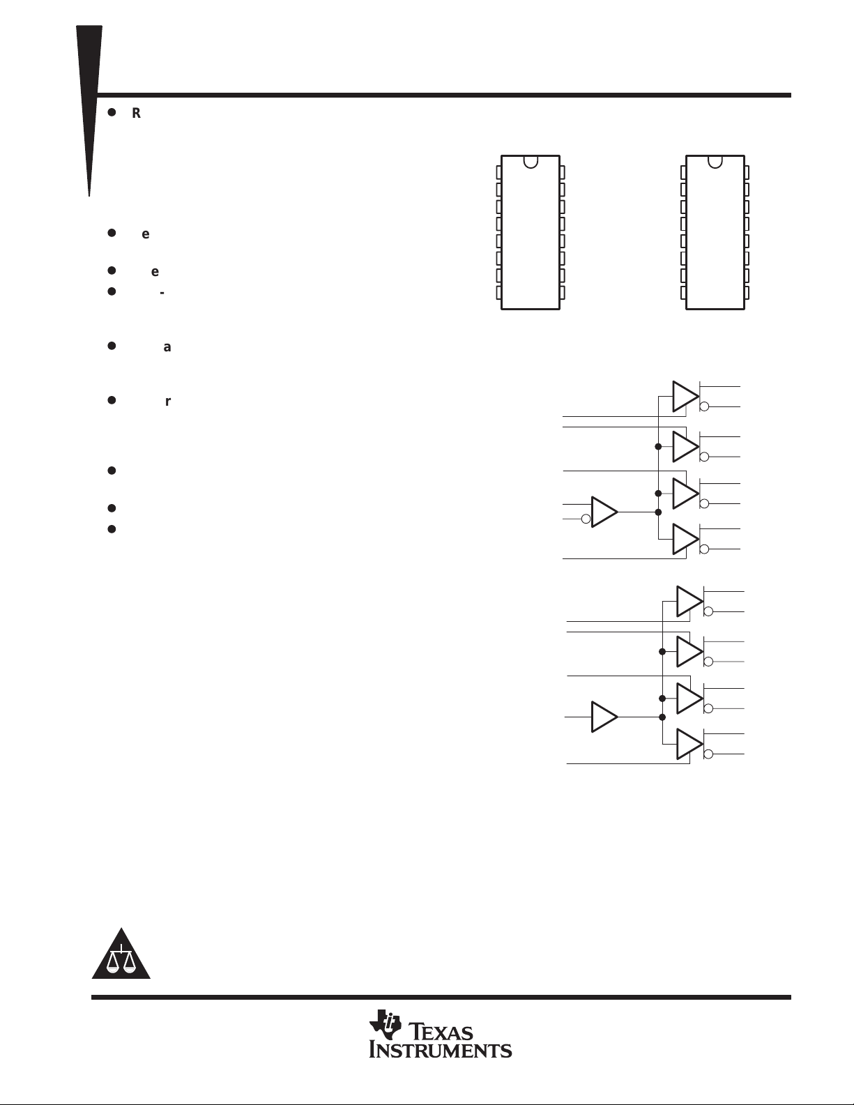
4Z
4Y
3Z
3Y
2Z
2Y
1Z
1Y
EN1
EN2
A
’LVDS104
EN4
logic diagram (positive logic)
EN3
B
4Z
4Y
3Z
3Y
2Z
2Y
1Z
1Y
EN1
EN2
A
’LVDS105
EN4
EN3
1
2
3
4
5
6
7
8
16
15
14
13
12
11
10
9
EN1
EN2
EN3
V
CC
GND
A
B
EN4
1Y
1Z
2Y
2Z
3Y
3Z
4Y
4Z
SN65LVDS104
D OR PW PACKAGE
(TOP VIEW)
1
2
3
4
5
6
7
8
16
15
14
13
12
11
10
9
EN1
EN2
EN3
V
CC
GND
A
NC
EN4
1Y
1Z
2Y
2Z
3Y
3Z
4Y
4Z
SN65LVDS105
D OR PW PACKAGE
(TOP VIEW)
SN65LVDS104, SN65LVDS105
4-PORT LVDS AND 4-PORT TTL-TO-LVDS REPEATERS
SLLS396B– SEPTEMBER 1999 – REVISED DECEMBER 1999
2
POST OFFICE BOX 655303 • DALLAS, TEXAS 75265
description (continued)
The SN65LVDS104 and SN65LVDS105 are members of a family of LVDS repeaters. A brief overview of the
family is provided in the table below.
Selection Guide to L VDS Repeaters
DEVICE
NO. INPUTS NO. OUTPUTS PACKAGE COMMENT
SN65LVDS22 2 LVDS 2 LVDS 16-pin D Dual multiplexed LVDS repeater
SN65LVDS104 1 LVDS 4 LVDS 16-pin D 4-Port LVDS repeater
SN65LVDS105 1 LVTTL 4 LVDS 16-pin D 4-Port TTL-to-LVDS repeater
SN65LVDS108 1 LVDS 8 LVDS 38-pin DBT 8-Port LVDS repeater
SN65LVDS109 2 LVDS 8 LVDS 38-pin DBT Dual 4-port LVDS repeater
SN65LVDS116 1 LVDS 16 LVDS 64-pin DGG 16-Port LVDS repeater
SN65LVDS117 2 LVDS 16 LVDS 64-pin DGG Dual 8-port LVDS repeater
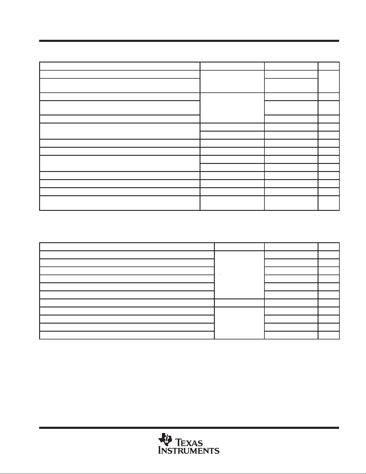
Function Tables
SN65LVDS104 SN65LVDS105
INPUT
OUTPUT INPUT OUTPUT
V
ID
= V
A
- V
B
#EN #Y #Z A #EN #Y #Z
X X Z Z L H L H
X L Z Z H H H L
V
ID
≥ 100 mV H H L Open H L H
–100 mV < V
ID
< 100 mV H ? ? X L Z Z
V
ID
≤ –100 mV H L H X X Z Z
H = high level, L = low level, Z = high impedance, ? = indeterminate, X = don’t care
equivalent input and output schematic diagrams
300 kΩ300 kΩ
V
CC
7 V 7 V
A
Input
B
Input
7 V
300 kΩ
50 Ω
V
CC
EN and
A (’LVDS105)
Input
V
CC
5 Ω
7 V
Y or Z
Output
10 kΩ
SN65LVDS104, SN65LVDS105
4-PORT LVDS AND 4-PORT TTL-TO-LVDS REPEATERS
SLLS396B– SEPTEMBER 1999 – REVISED DECEMBER 1999
3
POST OFFICE BOX 655303 • DALLAS, TEXAS 75265
absolute maximum ratings over operating free-air temperature (unless otherwise noted)
†
Supply voltage range, V
CC
(see Note 1) –0.5 to 4 V. . . . . . . . . . . . . . . . . . . . . . . . . . . . . . . . . . . . . . . . . . . . . . . . .
Voltage range, Enable inputs –0.5 to 6 V. . . . . . . . . . . . . . . . . . . . . . . . . . . . . . . . . . . . . . . . . . . . . . . . . . . .
A, B, Y or Z –0.5 to 4 V. . . . . . . . . . . . . . . . . . . . . . . . . . . . . . . . . . . . . . . . . . . . . . . . . . . . . .
Electrostatic discharge (see Note 2); Y, Z, and GND Class 3, A:16 kV, B: 600 V. . . . . . . . . . . . . . . . . . . . . . . .
All pins Class 3, A:7 kV, B: 500 V. . . . . . . . . . . . . . . . . . . . . . . . . . . . . . . .
Continuous power dissipation See Dissipation Rating Table. . . . . . . . . . . . . . . . . . . . . . . . . . . . . . . . . . . . . . . . .
Storage temperature range –65°C to 150°C. . . . . . . . . . . . . . . . . . . . . . . . . . . . . . . . . . . . . . . . . . . . . . . . . . . . . . . .
Lead temperature 1,6 mm (1/16 inch) from case for 10 seconds 260°C. . . . . . . . . . . . . . . . . . . . . . . . . . . . . . .
†
Stresses beyond those listed under “absolute maximum ratings” may cause permanent damage to the device. These are stress ratings only, and
functional operation of the device at these or any other conditions beyond those indicated under “recommended operating conditions” is not
implied. Exposure to absolute-maximum-rated conditions for extended periods may affect device reliability.
NOTES: 1. All voltage values, except differential I/O bus voltages, are with respect to network ground terminal.
2. T ested in accordance with MIL-STD-883C Method 3015.7
DISSIPATION RATING TABLE
PACKAGE
T
A
≤ 25°C
POWER RATING
OPERATING FACTOR‡
ABOVE T
A
= 25°C
T
A
= 85°C
POWER RATING
D 950 mW 7.6 mW/°C 494 mW
PW 774 mW 6.2 mW/°C 402 mW
‡
This is the inverse of the junction-to-ambient thermal resistance when board-mounted (low-k)
and with no air flow.
recommended operating conditions
MIN NOM MAX UNIT
Supply voltage, V
CC
3 3.3 3.6 V
High-level input voltage, V
IH
2 V
Low-level input voltage, V
IL
0.8 V
Magnitude of differential input voltage, V
ID
0.1 3.6 V
Common-mode input voltage, V
IC
Ť
V
ID
Ť
2
2.4 –
Ť
V
ID
Ť
2
V
g
IC
V
CC
–0.8 V
Operating free-air temperature, T
A
–40 85 °C
SN65LVDS104, SN65LVDS105
4-PORT LVDS AND 4-PORT TTL-TO-LVDS REPEATERS
SLLS396B– SEPTEMBER 1999 – REVISED DECEMBER 1999
4
POST OFFICE BOX 655303 • DALLAS, TEXAS 75265
SN65LVDS104 electrical characteristics over recommended operating conditions (unless
otherwise noted)
PARAMETER TEST CONDITIONS MIN TYP
†
MAX UNIT
V
ITH+
Positive-going differential input voltage threshold
100
V
ITH–
Negative-going differential input voltage threshold
See
Fig
u
re
1
and
Table
1
–100
mV
V
OD
Differential output voltage magnitude
R
= 100Ω,
247 340 454
∆V
OD
Change in differential output voltage magnitude between
logic states
L
,
V
ID
= ± 100 mV,
See Figure 1 and Figure 2
–50 50
mV
V
OC(SS)
Steady-state common-mode output voltage 1.125 1.375 V
∆V
OC(SS)
Change in steady-state common-mode output voltage
between logic states
See Figure 3
–50 50 mV
V
OC(PP)
Peak-to-peak common-mode output voltage 25 150 mV
pp
Enabled, R
L
= 100Ω 23 35 mA
I
CC
S
u
ppl
y
c
u
rrent
Disabled 3 8 mA
p
p
V
I
= 0 V –2 –11 –20
I
I
Inp
u
t
c
u
rrent
(A
or
B
inp
u
ts)
V
I
= 2.4 V –1.2 –3
µ
A
I
I(OFF)
Power-off Input current V
CC
= 1.5 V, V
I
= 2.4 V 20 µA
I
IH
High-level input current (enables) V
IH
= 2 V 20 µA
I
IL
Low-level input current (enables) V
IL
= 0.8 V 10 µA
p
V
OY
or V
OZ
= 0 V ±10 mA
I
OS
Short
-
circ
u
it
o
u
tp
u
t
c
u
rrent
V
OD
= 0 V ±10 mA
I
OZ
High-impedance output current V
O
= 0 V or 2.4 V ±1 µA
I
O(OFF)
Power-off output current V
CC
= 1.5 V, V
O
= 2.4 V ±1 µA
C
IN
Input capacitance (A or B inputs) V
I
= 0.4 sin (4E6πt) + 0.5 V 3 pF
C
O
Output capacitance (Y or Z outputs)
V
I
= 0.4 sin (4E6πt) + 0.5 V,
Disabled
9.4 pF
†
All typical values are at 25°C and with a 3.3 V supply.
SN65LVDS104 switching characteristics over recommended operating conditions (unless
otherwise noted)
PARAMETER TEST CONDITIONS MIN TYP
†
MAX UNIT
t
PLH
Propagation delay time, low-to-high-level output 2.4 3.2 4.2 ns
t
PHL
Propagation delay time, high-to-low-level output 2.2 3.1 4.2 ns
t
r
Differential output signal rise time
R
L
= 100Ω,
p
0.3 0.8 1.2 ns
t
f
Differential output signal fall time
C
L
=
10
p
F
,
See
Fi
gu
r
e
4
0.3 0.8 1.2 ns
t
sk(p)
Pulse skew (|t
PHL
– t
PLH
|)
See
Figure
4
150 500 ps
t
sk(o)
Channel-to-channel output skew
‡
20 100 ps
t
sk(pp)
Part-to-part skew
§
1.5 ns
t
PZH
Propagation delay time, high-impedance-to-high-level output 7.2 15 ns
t
PZL
Propagation delay time, high-impedance-to-low-level output
8.4 15 ns
t
PHZ
Propagation delay time, high-level-to-high-impedance output
See
Fig
u
re
5
3.6 15 ns
t
PLZ
Propagation delay time, low-level-to-high-impedance output 6 15 ns
†
All typical values are at 25°C and with a 3.3 V supply.
‡
t
sk(o)
is the magnitude of the time difference between the t
PLH
or t
PHL
of all drivers of a single device with all of their inputs connected together.
§
t
sk(pp)
is the magnitude of the difference in propagation delay times between any specified terminals of two devices when both devices operate
with the same supply voltages, at the same temperature, and have identical packages and test circuits.
SN65LVDS104, SN65LVDS105
4-PORT LVDS AND 4-PORT TTL-TO-LVDS REPEATERS
SLLS396B– SEPTEMBER 1999 – REVISED DECEMBER 1999
5
POST OFFICE BOX 655303 • DALLAS, TEXAS 75265
SN65LVDS105 electrical characteristics over recommended operating conditions (unless
otherwise noted)
PARAMETER TEST CONDITIONS MIN TYP
†
MAX UNIT
V
OD
Differential output voltage magnitude
R
= 100Ω,
247 340 454
∆V
OD
Change in differential output voltage magnitude between
logic states
L
,
V
ID
= ± 100 mV,
See Figure 6 and Figure 7
–50 50
mV
V
OC(SS)
Steady-state common-mode output voltage 1.125 1.375 V
∆V
OC(SS)
Change in steady-state common-mode output voltage be-
tween logic states
See Figure 8
–50 50 mV
V
OC(PP)
Peak-to-peak common-mode output voltage 25 150 mV
pp
Enabled, R
L
= 100Ω 23 35 mA
I
CC
S
u
ppl
y
c
u
rrent
Disabled 0.7 6.4 mA
I
IH
High-level input current V
IH
= 2 V 20 µA
I
IL
Low-level input current V
IL
= 0.8 V 10 µA
p
V
OY
or V
OZ
= 0 V ±10 mA
I
OS
Short
-
circ
u
it
o
u
tp
u
t
c
u
rrent
V
OD
= 0 V ±10 mA
I
OZ
High-impedance output current V
O
= 0 V or 2.4 V ±1 µA
I
O(OFF)
Power-off output current V
CC
= 1.5 V, V
O
= 2.4 V 0.3 ±1 µA
C
IN
Input capacitance V
I
= 0.4 sin (4E6πt) + 0.5 V 5 pF
C
O
Output capacitance (Y or Z outputs)
V
I
= 0.4 sin (4E6πt) + 0.5 V,
Disabled
9.4 pF
†
All typical values are at 25°C and with a 3.3 V supply.
SN65LVDS105 switching characteristics over recommended operating conditions (unless
otherwise noted)
PARAMETER TEST CONDITIONS MIN TYP
†
MAX UNIT
t
PLH
Propagation delay time, low-to-high-level output 1.7 2.2 3 ns
t
PHL
Propagation delay time, high-to-low-level output 1.4 2.3 3.5 ns
t
r
Differential output signal rise time
R
L
= 100Ω,
p
0.3 0.8 1.2 ns
t
f
Differential output signal fall time
C
L
=
10
p
F
,
See
Fi
gu
r
e
9
0.3 0.8 1.2 ns
t
sk(p)
Pulse skew (|t
PHL
– t
PLH
|)
See
Figure
9
150 500 ps
t
sk(o)
Channel-to-channel output skew
‡
20 100 ps
t
sk(pp)
Part-to-part skew
§
1.5 ns
t
PZH
Propagation delay time, high-impedance-to-high-level output 7.2 15 ns
t
PZL
Propagation delay time, high-impedance-to-low-level output
8.4 15 ns
t
PHZ
Propagation delay time, high-level-to-high-impedance output
See
Fig
u
re
10
3.6 15 ns
t
PLZ
Propagation delay time, low-level-to-high-impedance output 6 15 ns
†
All typical values are at 25°C and with a 3.3 V supply.
‡
t
sk(o)
is the magnitude of the time difference between the t
PLH
or t
PHL
of all drivers of a single device with all of their inputs connected together.
§
t
sk(pp)
is the magnitude of the difference in propagation delay times between any specified terminals of two devices when both devices operate
with the same supply voltages, at the same temperature, and have identical packages and test circuits.
SN65LVDS104, SN65LVDS105
4-PORT LVDS AND 4-PORT TTL-TO-LVDS REPEATERS
SLLS396B– SEPTEMBER 1999 – REVISED DECEMBER 1999
6
POST OFFICE BOX 655303 • DALLAS, TEXAS 75265
PARAMETER MEASUREMENT INFORMATION
I
I
V
IB
V
ID
V
IA
A
B
I
IB
V
OD
V
OZ
V
OY
V
OC
I
OY
I
OZ
Z
Y
V
OY
)
V
OZ
2
Figure 1. ’LVDS104 Voltage and Current Definitions
Table 1. SN65LVDS104 Minimum and Maximum Input Threshold Test Voltages
APPLIED
VOLTAGES
RESULTING
DIFFERENTIAL
INPUT VOLTAGE
RESULTING
COMMON-MODE
INPUT VOLTAGE
V
IA
V
IB
V
ID
V
IC
1.25 V 1.15 V 100 mV 1.2 V
1.15 V 1.25 V –100 mV 1.2 V
2.4 V 2.3 V 100 mV 2.35 V
2.3 V 2.4 V –100 mV 2.35 V
0.1 V 0 V 100 mV 0.05 V
0 V 0.1 V –100 mV 0.05 V
1.5 V 0.9 V 600 mV 1.2 V
0.9 V 1.5 V –600 mV 1.2 V
2.4 V 1.8 V 600 mV 2.1 V
1.8 V 2.4 V –600 mV 2.1 V
0.6 V 0 V 600 mV 0.3 V
0 V 0.6 V –600 mV 0.3 V
±
3.75 kΩ
0 V ≤ V
TEST
≤ 2.4 V
Y
Z
V
OD
Input
100 Ω
3.75 kΩ
Figure 2. ’LVDS104 VOD Test Circuit
 Loading...