


Texas Instruments SN74ABT646DBLE, SN74ABT646DBR, SN74ABT646DGVR, SN74ABT646DW, SN74ABT646DWR Datasheet
...•State-of-the-Art EPIC-ΙΙB BiCMOS Design
Significantly Reduces Power Dissipation
•ESD Protection Exceeds 2000 V Per MIL-STD-883C, Method 3015; Exceeds 200 V Using Machine Model (C = 200 pF, R = 0)
•Latch-Up Performance Exceeds 500 mA Per JEDEC Standard JESD-17
•Typical VOLP (Output Ground Bounce) < 1 V at VCC = 5 V, TA = 25°C
•High-Drive Outputs (±32-mA IOH, 64-mA IOL )
•Package Options Include Plastic Small-Outline (DW), Shrink Small-Outline (DB), and Thin Shrink Small-Outline (PW) Packages, Ceramic Chip Carriers (FK), and Plastic (NT) and Ceramic (JT) DIPs
description
These devices consist of bus transceiver circuits, D-type flip-flops, and control circuitry arranged for multiplexed transmission of data directly from the input bus or from the internal registers. Data on the A or B bus is clocked into the registers on the low-to-high transition of the appropriate clock (CLKAB or CLKBA) input. Figure 1 illustrates the four fundamental bus-management functions that can be performed with the ′ABT646.
Output-enable (OE) and direction-control (DIR) inputs are provided to control the transceiver functions. In the transceiver mode, data present at the high-impedance port may be stored in either register or in both.
SN54ABT646, SN74ABT646 OCTAL BUS TRANSCEIVERS AND REGISTERS WITH 3-STATE OUTPUTS
SCBS068E ± JULY 1991 ± REVISED JULY 1994
SN54ABT646 . . . JT PACKAGE
SN74ABT646 . . . DB, DW, NT, OR PW PACKAGE
|
|
|
|
|
|
|
|
(TOP VIEW) |
|
|
|
|
|
|
|
|
|||||||
CLKAB |
|
|
|
|
|
|
|
|
|
VCC |
|
||||||||||||
|
|
1 |
|
|
|
|
24 |
|
|
||||||||||||||
|
|
|
|
|
|
|
|
||||||||||||||||
|
|
|
|
|
|
|
|
||||||||||||||||
|
|
|
|
SAB |
|
|
2 |
|
|
|
|
23 |
|
|
CLKBA |
|
|||||||
|
|
|
|
DIR |
|
|
3 |
|
|
|
|
22 |
|
|
SBA |
|
|||||||
|
|
|
|
|
|
|
|
|
|
|
|
|
|||||||||||
|
|
|
|
|
A1 |
|
|
|
|
|
|
|
|
|
|
|
|
|
|
|
|
|
|
|
|
|
|
|
|
|
4 |
|
|
|
|
21 |
|
|
OE |
|
|
|
|
||||
|
|
|
|
|
A2 |
|
|
5 |
|
|
|
|
20 |
|
|
B1 |
|
||||||
|
|
|
|
|
|
|
|
|
|
|
|
|
|
||||||||||
|
|
|
|
|
A3 |
|
|
6 |
|
|
|
|
19 |
|
|
B2 |
|
||||||
|
|
|
|
|
|
|
|
|
|
|
|
|
|
||||||||||
|
|
|
|
|
A4 |
|
|
7 |
|
|
|
|
18 |
|
|
B3 |
|
||||||
|
|
|
|
|
|
|
|
|
|
|
|
|
|
||||||||||
|
|
|
|
|
A5 |
|
|
8 |
|
|
|
|
17 |
|
|
B4 |
|
||||||
|
|
|
|
|
|
|
|
|
|
|
|
|
|
||||||||||
|
|
|
|
|
A6 |
|
|
9 |
|
|
|
|
16 |
|
|
B5 |
|
||||||
|
|
|
|
|
|
|
|
|
|
|
|
|
|
||||||||||
|
|
|
|
|
A7 |
|
|
10 |
|
|
|
15 |
|
|
B6 |
|
|||||||
|
|
|
|
|
|
|
|
|
|
|
|
|
|||||||||||
|
|
|
|
|
A8 |
|
|
11 |
|
|
|
14 |
|
|
B7 |
|
|||||||
|
|
|
|
|
|
|
|
|
|
|
|
|
|||||||||||
|
|
|
|
GND |
|
|
12 |
|
|
|
13 |
|
|
B8 |
|
||||||||
|
|
|
|
|
|
|
|
|
|
|
|
||||||||||||
|
|
|
|
|
|
|
|
|
|
|
|
|
|
|
|
|
|
|
|
|
|
|
|
|
SN54ABT646 . . . FK PACKAGE |
|
|||||||||||||||||||||
|
|
|
|
|
|
|
|
|
(TOP VIEW) |
CLKBA |
|
|
|
|
|
||||||||
|
|
|
|
|
DIR |
SAB |
CLKAB |
NC |
V |
SBA |
|
||||||||||||
|
|
|
|
|
|
|
|
|
|
|
|
|
|
|
CC |
|
|
|
|
|
|
|
|
|
|
|
|
|
|
|
|
|
|
|
|
|
|
|
|
|
|
|
|
|
|
|
|
|
|
|
|
4 |
|
3 |
|
|
2 |
|
1 |
|
28 |
27 26 |
|
|
|
||||||
A1 |
|
|
|
5 |
|
|
|
|
|
|
|
|
|
|
|
|
|
|
25 |
|
|
OE |
|
A2 |
|
|
|
|
|
|
|
|
|
|
|
|
|
|
|
|
|
|
24 |
|
|
B1 |
|
|
|
|
6 |
|
|
|
|
|
|
|
|
|
|
|
|
|
|
|
|
||||
A3 |
|
|
|
|
|
|
|
|
|
|
|
|
|
|
|
|
|
|
23 |
|
|
B2 |
|
|
|
|
7 |
|
|
|
|
|
|
|
|
|
|
|
|
|
|
|
|
||||
NC |
|
|
|
|
|
|
|
|
|
|
|
|
|
|
|
|
|
|
22 |
|
|
NC |
|
|
|
|
8 |
|
|
|
|
|
|
|
|
|
|
|
|
|
|
|
|
||||
A4 |
|
|
|
9 |
|
|
|
|
|
|
|
|
|
|
|
|
|
|
21 |
|
|
B3 |
|
A5 |
|
|
|
|
|
|
|
|
|
|
|
|
|
|
|
|
|
|
20 |
|
|
B4 |
|
|
|
|
10 |
|
|
|
|
|
|
|
|
|
|
|
|
|
|
|
|||||
A6 |
|
|
|
|
|
|
|
|
|
|
|
|
|
|
|
|
|
|
1819 |
|
|
B5 |
|
|
|
|
1112 13 14 15 16 17 |
|
|
|
|||||||||||||||||
|
|
|
|
|
|||||||||||||||||||
|
|
|
|
|
|
||||||||||||||||||
|
|
|
|
|
|
|
|
|
|
|
|
|
|
|
|
|
|
|
|
|
|
|
|
|
|
|
|
|
A7 |
|
A8 |
GND |
NC |
B8 |
|
B7 |
B6 |
|
|||||||||
NC ± No internal connection |
|
|
|
|
|
||||||||||||||||||
The select-control (SAB and SBA) inputs can multiplex stored and real-time (transparent mode) data. The direction control (DIR) determines which bus will receive data when OE is low. In the isolation mode (OE high), A data may be stored in one register and/or B data may be stored in the other register.
When an output function is disabled, the input function is still enabled and may be used to store and transmit data. Only one of the two buses, A or B, may be driven at a time.
To ensure the high-impedance state during power up or power down, OE should be tied to VCC through a pullup resistor; the minimum value of the resistor is determined by the current-sinking capability of the driver.
The SN74ABT646 is available in TI's shrink small-outline package (DB), which provides the same I/O pin count and functionality of standard small-outline packages in less than half the printed-circuit-board area.
The SN54ABT646 is characterized for operation over the full military temperature range of ±55°C to 125°C. The SN74ABT646 is characterized for operation from ±40°C to 85°C.
EPIC-ΙΙB is a trademark of Texas Instruments Incorporated.
UNLESS OTHERWISE NOTED this document contains PRODUCTION DATA information current as of publication date. Products conform to specifications per the terms of Texas Instruments standard warranty. Production processing does not necessarily include testing of all parameters.
Copyright 1994, Texas Instruments Incorporated
POST OFFICE BOX 655303 •DALLAS, TEXAS 75265 |
2±1 |

SN54ABT646, SN74ABT646
OCTAL BUS TRANSCEIVERS AND REGISTERS
WITH 3-STATE OUTPUTS
SCBS068E ± JULY 1991 ± REVISED JULY 1994
BUS A |
BUS B |
BUS A |
BUS B |
21 |
3 |
1 |
23 |
2 |
22 |
21 |
3 |
1 |
23 |
2 |
22 |
|
OE |
DIR |
CLKAB CLKBA |
SAB |
SBA |
|
OE |
DIR |
CLKAB |
CLKBA |
SAB |
SBA |
|
L |
L |
X |
X |
X |
L |
|
L |
H |
X |
X |
L |
X |
|
REAL-TIME TRANSFER |
|
|
|
|
REAL-TIME TRANSFER |
|
|||||
|
|
BUS B TO BUS A |
|
|
|
|
|
BUS A TO BUS B |
|
|
||
BUS A |
BUS B |
BUS A |
BUS B |
21 |
3 |
1 |
23 |
2 |
22 |
21 |
3 |
1 |
23 |
2 |
22 |
OE |
DIR |
CLKAB CLKBA |
SAB |
SBA |
OE |
DIR |
CLKAB |
CLKBA |
SAB |
SBA |
|
X |
X |
↑ |
X |
X |
X |
L |
L |
X |
L |
X |
H |
X |
X |
X |
↑ |
X |
X |
L |
H |
L |
X |
H |
X |
H |
X |
↑ |
↑ |
X |
X |
|
|
|
|
|
|
|
|
STORAGE FROM |
|
|
|
TRANSFER STORED DATA |
|
||||
|
|
A, B, OR A AND B |
|
|
|
|
TO A AND/OR B |
|
|
||
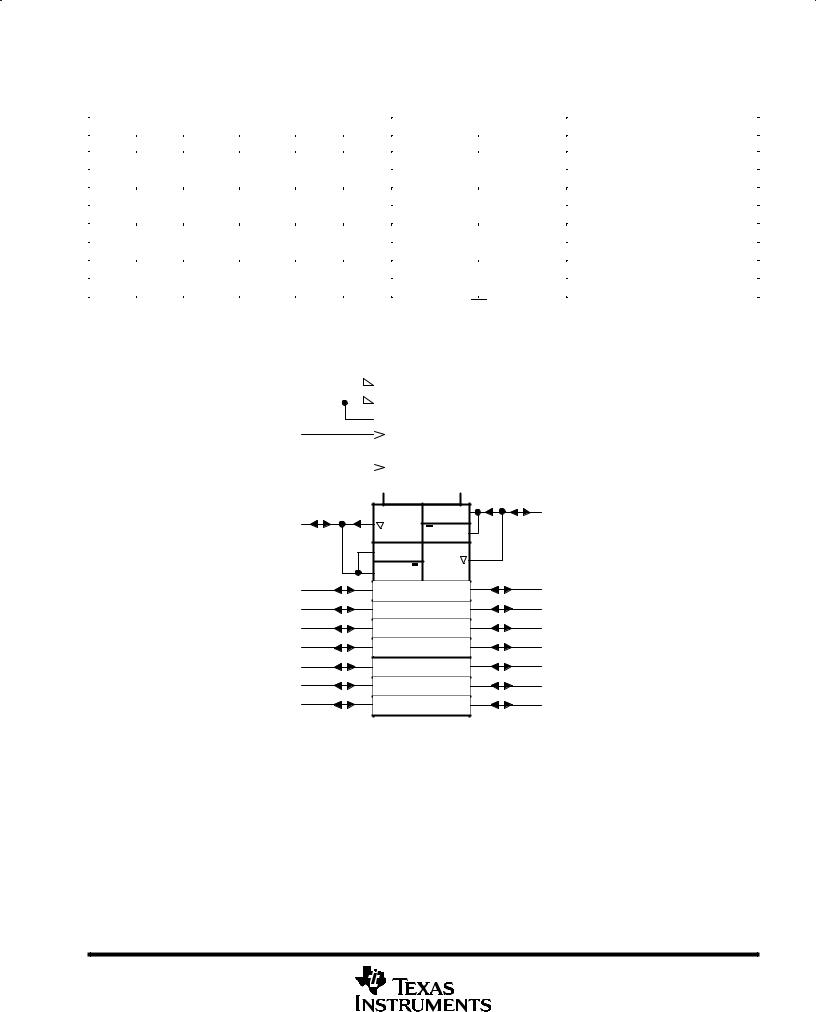
Figure 1. Bus-Management Functions
Pin numbers shown are for DB, DW, JT, NT, and PW packages.
2±2 |
POST OFFICE BOX 655303 •DALLAS, TEXAS 75265 |
SN54ABT646, SN74ABT646
OCTAL BUS TRANSCEIVERS AND REGISTERS
WITH 3-STATE OUTPUTS
|
|
|
|
|
|
|
|
|
SCBS068E ± JULY 1991 ± REVISED JULY 1994 |
||
|
|
|
|
|
|
|
|
|
|
|
|
|
|
|
|
|
|
FUNCTION TABLE |
|
|
|
|
|
|
|
|
|
|
|
|
|
|
|
||
|
|
|
INPUTS |
|
|
DATA I/Os |
|
OPERATION OR FUNCTION |
|||
|
|
|
|
|
|
|
|
|
|
||
|
OE |
DIR |
CLKAB |
CLKBA |
SAB |
SBA |
A1 THRU A8 |
B1 THRU B8 |
|
||
|
|
|
|
||||||||
|
|
|
|
|
|
|
|
|
|
|
|
|
X |
X |
↑ |
X |
X |
X |
Input |
Unspecified² |
|
Store A, B unspecified² |
|
|
X |
X |
X |
↑ |
X |
X |
Unspecified² |
Input |
|
Store B, A unspecified² |
|
|
H |
X |
↑ |
↑ |
X |
X |
Input |
Input |
|
Store A and B data |
|
|
H |
X |
H or L |
H or L |
X |
X |
Input disabled |
Input disabled |
|
Isolation, hold storage |
|
|
|
|
|
|
|
|
|
|
|
|
|
|
L |
L |
X |
X |
X |
L |
Output |
Input |
|
Real-time B data to A bus |
|
|
L |
L |
X |
H or L |
X |
H |
Output |
Input |
|
Stored B data to A bus |
|
|
|
|
|
|
|
|
|
|
|
|
|
|
L |
H |
X |
X |
L |
X |
Input |
Output |
|
Real-time A data to B bus |
|
|
L |
H |
H or L |
X |
H |
X |
Input |
Output |
|
Stored A data to B bus |
|
|
|
|
|
|
|
|
|
|
|
|
|
²The data output functions may be enabled or disabled by various signals at the OE and DIR inputs. Data input functions are always enabled; i.e., data at the bus pins will be stored on every low-to-high transition of the clock inputs.
logic symbol³
|
|
21 |
|
|
|
G3 |
|||
|
OE |
|
|
|
|
|
|||
|
3 |
|
|
|
|||||
DIR |
|
|
|
3 EN1 [BA] |
|||||
|
|
|
|
|
|||||
|
|
23 |
|
|
|
3 EN2 [AB] |
|||
CLKBA |
|
|
|
|
C4 |
||||
22 |
|
|
|
|
|||||
SBA |
|
|
|
G5 |
|||||
|
|
|
|
|
|||||
1 |
|
|
|
||||||
CLKAB |
|
|
|
|
C6 |
||||
|
|
|
|
|
|
||||
2 |
|
|
|
|
|||||
SAB |
|
|
|
G7 |
|||||
|
|
|
|
|
|||||
|
|
|
|
|
|||||
|
|
|
|
|
|
|
|
|
|
|
|
|
|
|
20 |
4 |
≥ |
1 |
5 |
4D |
B1 |
A1 |
1 |
|
5 |
1 |
|
|
|
|
|
||
|
6D |
|
7 |
≥ 1 |
|
|
1 |
|
7 |
2 |
|
5 |
|
|
19 |
||
|
|
|
|
||
A2 |
|
|
|
|
|
|
|
|
|
B2 |
|
6 |
|
|
|
|
18 |
A3 |
|
|
|
|
B3 |
7 |
|
|
|
|
17 |
A4 |
|
|
|
|
B4 |
8 |
|
|
|
|
16 |
A5 |
|
|
|
|
B5 |
9 |
|
|
|
|
15 |
A6 |
|
|
|
|
B6 |
10 |
|
|
|
|
14 |
A7 |
|
|
|
|
B7 |
11 |
|
|
|
|
13 |
A8 |
|
|
|
|
B8 |
³ This symbol is in accordance with ANSI/IEEE Std 91-1984 and IEC Publication 617-12. Pin numbers shown are for the DB, DW, JT, NT, and PW packages.
POST OFFICE BOX 655303 •DALLAS, TEXAS 75265 |
2±3 |
 Loading...