


SN65LVDS32NSR
Texas Instruments SN65LVDS32NSR, SN65LVDS3486D, SN65LVDS3486DR, SNJ55LVDS32FK, SNJ55LVDS32J Datasheet
...
SN55LVDS32, SN65LVDS32, SN65LVDS3486, SN65LVDS9637
HIGH-SPEED DIFFERENTIAL LINE RECEIVERS
SLLS262H – JULY 1997 – REVISED MARCH 2000
1
POST OFFICE BOX 655303 • DALLAS, TEXAS 75265
D
Meets or Exceeds the Requirements of
ANSI TIA/EIA-644 Standard
D
Operates with a Single 3.3-V Supply
D
Designed for Signaling Rate of Up To
400 Mbps
D
Differential Input Thresholds ±100 mV Max
D
Typical Propagation Delay Time of 2.1 ns
D
Power Dissipation 60 mW Typical per
Receiver at 200 MHz
D
Bus-T erminal ESD Protection Exceeds 8 kV
D
Low-Voltage TTL (LVTTL) Logic Output
Levels
D
Pin-Compatible with the AM26LS32,
MC3486, and µA9637
D
Open-Circuit Fail Safe
description
The SN55LVDS32, SN65LVDS32,
SN65LVDS3486, and SN65LVDS9637 are
differential line receivers that implement the
electrical characteristics of low-voltage differential
signaling (L VDS). This signaling technique lowers
the output voltage levels of 5-V differential
standard levels (such as EIA/TIA-422B) to reduce
the power, increase the switching speeds, and
allow operation with a 3.3-V supply rail. Any of the
four differential receivers provides a valid logical
output state with a ±100 mV differential input
voltage within the input common-mode voltage
range. The input common-mode voltage range
allows 1 V of ground potential difference between
two LVDS nodes.
The intended application of these devices and
signaling technique is both point-to-point and
multidrop (one driver and multiple receivers) data
transmission over controlled impedance media of
approximately 100 Ω. The transmission media
may be printed-circuit board traces, backplanes,
or cables. The ultimate rate and distance of data
transfer is dependent upon the attenuation
characteristics of the media and the noise
coupling to the environment.
The SN65LVDS32, SN65LVDS3486, and
SN65LVDS9637 are characterized for operation
from –40°C to 85°C. The SN55LVDS32 is
characterized for operation from –55°C to 125°C.
Copyright 2000, Texas Instruments Incorporated
PRODUCTION DATA information is current as of publication date.
Products conform to specifications per the terms of Texas Instruments
standard warranty. Production processing does not necessarily include
testing of all parameters.
Please be aware that an important notice concerning availability, standard warranty, and use in critical applications of
Texas Instruments semiconductor products and disclaimers thereto appears at the end of this data sheet.
1920132
17
18
16
15
14
1312119 10
5
4
6
7
8
4A
4Y
NC
G
3Y
1Y
G
NC
2Y
2A
1A1BNCV4B
GND
NC
3B
3A
2B
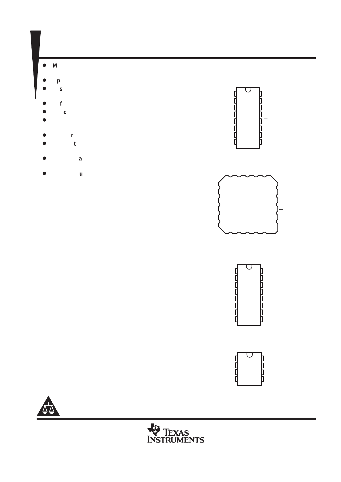
SN55LVDS32FK
(TOP VIEW)
CC
1
2
3
4
5
6
7
8
16
15
14
13
12
11
10
9
1B
1A
1Y
G
2Y
2A
2B
GND
V
CC
4B
4A
4Y
G
3Y
3A
3B
SN55LVDS32...J OR W
SN65LVDS32D
(Marked as LVDS32 or 65LVDS32)
(TOP VIEW)
1
2
3
4
5
6
7
8
16
15
14
13
12
11
10
9
1B
1A
1Y
1,2EN
2Y
2A
2B
GND
V
CC
4B
4A
4Y
3,4EN
3Y
3A
3B
SN65LVDS3486D (Marked as LVDS3486)
(TOP VIEW)
1
2
3
4
8
7
6
5
V
CC
1Y
2Y
GND
1A
1B
2A
2B
SN65LVDS9637D (Marked as DK637 or LVDS37)
SN65LVDS9637DGN (Marked as L37)
(TOP VIEW)
SN55LVDS32, SN65LVDS32, SN65LVDS3486, SN65LVDS9637
HIGH-SPEED DIFFERENTIAL LINE RECEIVERS
SLLS262H – JULY 1997 – REVISED MARCH 2000
2
POST OFFICE BOX 655303 • DALLAS, TEXAS 75265
AVAILABLE OPTIONS
PACKAGE
T
A
SMALL OUTLINE
(D)
MSOP
(DGN)
CHIP CARRIER
(FK)
CERAMIC DIP
(J)
FLAT PACK
(W)
SN65LVDS32D — — — —
–40°C to 85°C
SN65LVDS3486D — — — —
SN65LVDS9637D SN65LVDS9637DGN — — —
–55°C to 125°C — — SN55LVDS32FK SN55LVDS32J SN55LVDS32W
G
G
1A
1B
2A
2B
3A
3B
4A
4B
4
12
2
1
6
7
10
9
14
15
3
5
11
13
1Y
2Y
3Y
4Y
’L VDS32 logic diagram
(positive logic)
1A
1B
2A
2B
3A
3B
4A
4B
4
12
2
1
6
7
10
9
14
15
3
5
11
13
1Y
2Y
3Y
4Y
3,4EN
1,2EN
’L VDS3486D logic diagram
(positive logic)
1A
1B
2A
2B
8
7
6
5
2
3
1Y
2Y
’L VDS9637D logic diagram
(positive logic)
logic symbol
†
2Y
1Y
2B
2A
1B
1A
5
6
7
8
3
2
†
This symbol is in accordance with ANSI/IEEE Std
91-1984 and IEC Publication 617-12.
SN65LVDS9637
SN55LVDS32, SN65LVDS32, SN65LVDS3486, SN65LVDS9637
HIGH-SPEED DIFFERENTIAL LINE RECEIVERS
SLLS262H – JULY 1997 – REVISED MARCH 2000
3
POST OFFICE BOX 655303 • DALLAS, TEXAS 75265
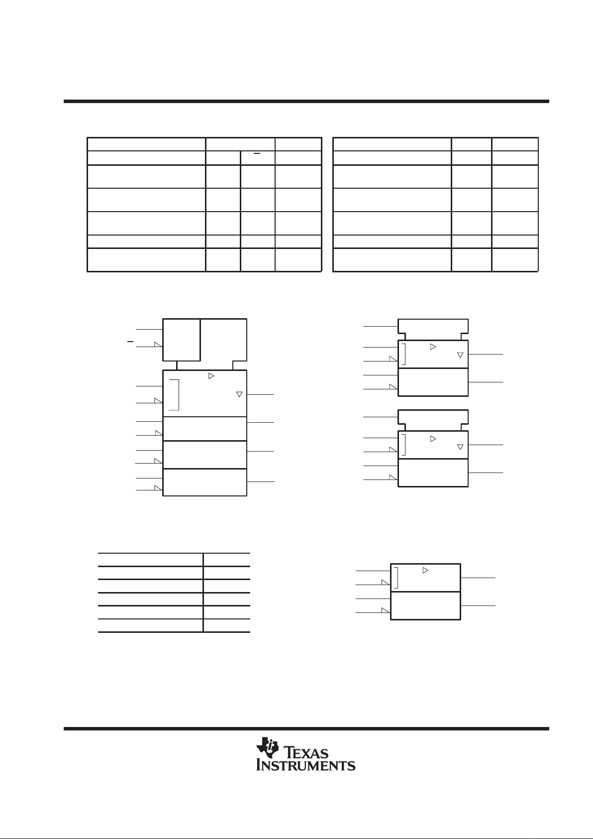
Function Tables
SN55LVDS32, SN65LVDS32 SN65LVDS3486
DIFFERENTIAL INPUT
ENABLES OUTPUT DIFFERENTIAL INPUT ENABLE OUTPUT
A, B G
G
Y A, B EN Y
VID ≥ 100 mV
H
X
X
L
H
H
VID ≥ 100 mV
H
X
H
H
–100 mV < VID < 100 mV
H
X
X
L
?
?
–100 mV < VID < 100 mV
H
X
?
?
VID ≤ –100 mV
H
X
X
L
L
L
VID ≤ –100 mV
H
X
L
L
X L H Z X L Z
Open
H
X
X
L
H
H
Open
H
X
H
H
H = high level, L = low level, X = irrelevant, Z = high impedance (off), ? = indeterminate
logic symbol
†
EN
≥ 1
G
G
1A
1B
2A
2B
3A
3B
4A
4B
3
5
11
13
1Y
2Y
3Y
4Y
4
12
2
1
6
7
10
9
14
15
†
This symbol is in accordance with ANSI/IEEE Std 91-1984 and IEC Publication 617-12.
EN
EN
4B
4A
3B
3A
3,4EN
13
11
4Y
3Y
15
14
9
10
12
2Y
1Y
2B
2A
1B
1A
1,2EN
7
6
1
2
4
5
3
SN65LVDS3486SN55LVDS32, SN65LVDS32
Function Table
SN65LVDS9637
DIFFERENTIAL INPUT
OUTPUT
A, B Y
VID ≥ 100 mV H
–100 mV < VID < 100 mV ?
VID ≤ –100 mV L
Open H
H = high level, L = low level, ? = indeterminate
SN55LVDS32, SN65LVDS32, SN65LVDS3486, SN65LVDS9637
HIGH-SPEED DIFFERENTIAL LINE RECEIVERS
SLLS262H – JULY 1997 – REVISED MARCH 2000
4
POST OFFICE BOX 655303 • DALLAS, TEXAS 75265
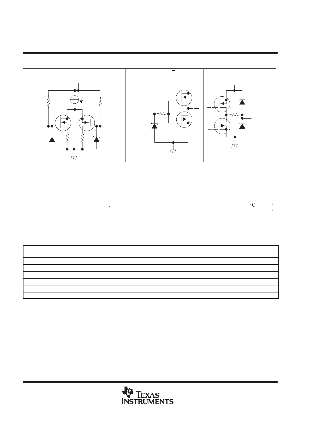
equivalent input and output schematic diagrams
300 kΩ300 kΩ
V
CC
7 V 7 V
A Input B Input
7 V
50 Ω
V
CC
Input
V
CC
5 Ω
7 V
Y Output
EQUIVALENT OF EACH A OR B INPUT EQUIVALENT OF G, G, 1,2EN OR
3,4EN INPUTS
TYPICAL OF ALL OUTPUTS
absolute maximum ratings over operating free-air temperature range (unless otherwise noted)
†
Supply voltage range, VCC (see Note 1) –0.5 V to 4 V. . . . . . . . . . . . . . . . . . . . . . . . . . . . . . . . . . . . . . . . . . . . . . . . . . . .
Input voltage range, V
I
–0.5 V to VCC + 0.5 V. . . . . . . . . . . . . . . . . . . . . . . . . . . . . . . . . . . . . . . . . . . . . . . . . . . . . .
Input voltage range, V
I
(A or B) –0.5 V to 4 V. . . . . . . . . . . . . . . . . . . . . . . . . . . . . . . . . . . . . . . . . . . . . . . . . . . . . . .
Continuous total power dissipation See Dissipation Rating Table. . . . . . . . . . . . . . . . . . . . . . . . . . . . . . . . . . . . . .
Storage temperature range, T
stg
–65_C to 150_C. . . . . . . . . . . . . . . . . . . . . . . . . . . . . . . . . . . . . . . . . . . . . . . . . . .
Lead temperature 1,6 mm (1/16 inch) from case for 10 seconds 260_C. . . . . . . . . . . . . . . . . . . . . . . . . . . . . . . .
†
Stresses beyond those listed under “absolute maximum ratings” may cause permanent damage to the device. These are stress ratings only, and
functional operation of the device at these or any other conditions beyond those indicated under “recommended operating conditions” is not
implied. Exposure to absolute-maximum-rated conditions for extended periods may affect device reliability.
NOTE 1: All voltages, except differential I/O bus voltages, are with respect to the network ground terminal.
DISSIPATION RATING TABLE
PACKAGE
TA ≤ 25°C
POWER RATING
DERATING FACTOR
‡
ABOVE TA = 25°C
TA = 70°C
POWER RATING
TA = 85°C
POWER RATING
TA = 125°C
POWER RATING
D (8) 725 mW 5.8 mW/°C 464 mW 377 mW —
D (16) 950 mW 7.6 mW/°C 608 mW 494 mW —
DGN 2.14 W 17.1 mW/°C 1.37 W 1.11 W —
FK 1375 mW 11.0 mW/°C 880 mW 715 mW 275 mW
J 1375 mW 11.0 mW/°C 880 mW 715 mW 275 mW
W 1000 mW 8.0 mW/°C 640 mW 520 mW 200 mW
‡
This is the inverse of the junction-to-ambient thermal resistance when board mounted and with no air flow.
SN55LVDS32, SN65LVDS32, SN65LVDS3486, SN65LVDS9637
HIGH-SPEED DIFFERENTIAL LINE RECEIVERS
SLLS262H – JULY 1997 – REVISED MARCH 2000
5
POST OFFICE BOX 655303 • DALLAS, TEXAS 75265
recommended operating conditions
MIN NOM MAX UNIT
Supply voltage, V
CC
3 3.3 3.6 V
High-level input voltage, V
IH
G, G, 1,2EN, or 3,4EN 2 V
Low-level input voltage, V
IL
G, G, 1,2EN, or 3,4EN 0.8 V
Magnitude of differential input voltage, |VID| 0.1 0.6 V
Common-mode input voltage, VIC (see Figure 1)
|VID|
2
2.4
*
|VID|
2
V
VCC – 0.8 V
p
p
SN65 prefix –40 85
°
Operating free-air temperature, T
A
SN55 prefix –55 125
°C
Max at VCC = 3 V
Max at VCC >3.15 V
Min
1
0.5
0
0 0.1 0.2 0.3
– Common Mode Input Voltage – V
1.5
2
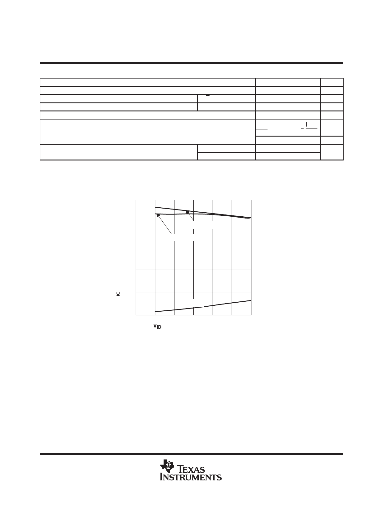
COMMON-MODE INPUT VOLTAGE RANGE
vs
DIFFERENTIAL INPUT VOLTAGE
2.5
0.4 0.5 0.6
V
IC
VID – Differential Input Voltage – V
Figure 1. VIC Versus VID and V
CC
SN55LVDS32, SN65LVDS32, SN65LVDS3486, SN65LVDS9637
HIGH-SPEED DIFFERENTIAL LINE RECEIVERS
SLLS262H – JULY 1997 – REVISED MARCH 2000
6
POST OFFICE BOX 655303 • DALLAS, TEXAS 75265
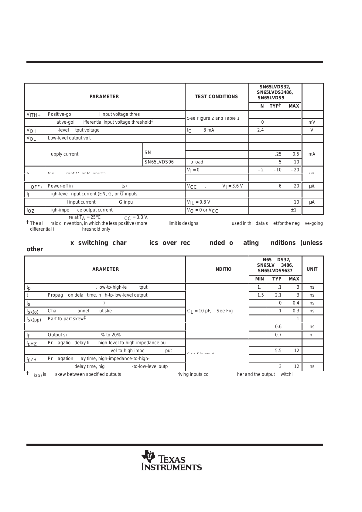
SN65LVDSxxxx electrical characteristics over recommended operating conditions (unless
otherwise noted)
БББББББББББББББББ
Á
PARAMETER
ББББББ
Á
TEST CONDITIONS
БББББ
Á
SN65LVDS32,
SN65LVDS3486,
SN65LVDS9637
Á
Á
UNIT
MIN
TYP†MAX
V
ITH+
ББББББББББББББББ
Positive-going differential input voltage threshold
100
mV
V
ITH–
ББББББББББББББББ
Negative-going differential input voltage threshold
‡
See Figure 2 and Table 1
–100
mV
V
OH
ББББББББББББББББ
High-level output voltage
IOH = –8 mA
2.4
V
V
OL
ББББББББББББББББ
Low-level output voltage
IOL = 8 mA
0.4
V
БББББББББББ
SN65LVDS32,
Enabled, No load
10
18
I
CC
БББББББББББ
Supply current
,
SN65LVDS3486
Disabled
0.25
0.5
mA
SN65LVDS9637
No load
5.5
10
ББББББББББББББББ
p
p
VI = 0
–2
–10
–20
I
I
ББББББББББББББББ
Input current (A or B inputs)
VI = 2.4 V
–1.2
–3
µ
A
I
I(OFF)
ББББББББББББББББ
Power-off input current (A or B inputs)
VCC = 0, VI = 3.6 V
6
20
µA
I
IH
ББББББББББББББББ
High-level input current (EN, G, or G inputs)
VIH = 2 V
10
µA
I
IL
ББББББББББББББББ
Low-level input current (EN, G, or G inputs)
VIL = 0.8 V
10
µA
I
OZ
ББББББББББББББББ
High-impedance output current
VO = 0 or V
CC
±10
µA
†
All typical values are at TA = 25°C and with VCC = 3.3 V.
‡
The algebraic convention, in which the less positive (more negative) limit is designated minimum, is used in this data sheet for the negative-going
differential input voltage threshold only.
SN65LVDSxxxx switching characteristics over recommended operating conditions (unless
otherwise noted)
БББББББББББББББББ
Á
PARAMETER
ББББББ
Á
TEST CONDITIONS
БББББ
Á
SN65LVDS32,
SN65LVDS3486,
SN65LVDS9637
Á
Á
UNIT
MIN
TYP
MAX
t
pLH
ББББББББББББББББ
Propagation delay time, low-to-high-level output
1.5
2.1
3
ns
t
pHL
ББББББББББББББББ
Propagation delay time, high-to-low-level output
1.5
2.1
3
ns
t
sk(p)
ББББББББББББББББ
Pulse skew (|t
PHL
– t
PLH
|)
0
0.4
ns
t
sk(o)
ББББББББББББББББ
Channel-to-channel output skew
†
CL = 10 pF, See Figure 3
0.1
0.3
ns
t
sk(pp)
ББББББББББББББББ
Part-to-part skew
‡
1
ns
t
r
ББББББББББББББББ
Output signal rise time, 20% to 80%
0.6
ns
t
f
Output signal fall time, 80% to 20%
0.7
ns
t
pHZ
ББББББББББББББББ
Propagation delay time, high-level-to-high-impedance output
6.5
12
ns
t
pLZ
ББББББББББББББББ
Propagation delay time, low-level-to-high-impedance output
5.5
12
ns
t
pZH
ББББББББББББББББ
Propagation delay time, high-impedance-to-high-level output
See Figure 4
8
12
ns
t
pZL
ББББББББББББББББ
Propagation delay time, high-impedance-to-low-level output
3
12
ns
†
t
sk(o)
is the skew between specified outputs of a single device with all driving inputs connected together and the outputs switching in the same
direction while driving identical specified loads.
‡
t
sk(pp)
is the magnitude of the different in propagation delay times between any specified terminals of two devices when both devices operate
with the same supply voltages, same temperature, and have identical packages and test circuits.
SN55LVDS32, SN65LVDS32, SN65LVDS3486, SN65LVDS9637
HIGH-SPEED DIFFERENTIAL LINE RECEIVERS
SLLS262H – JULY 1997 – REVISED MARCH 2000
7
POST OFFICE BOX 655303 • DALLAS, TEXAS 75265
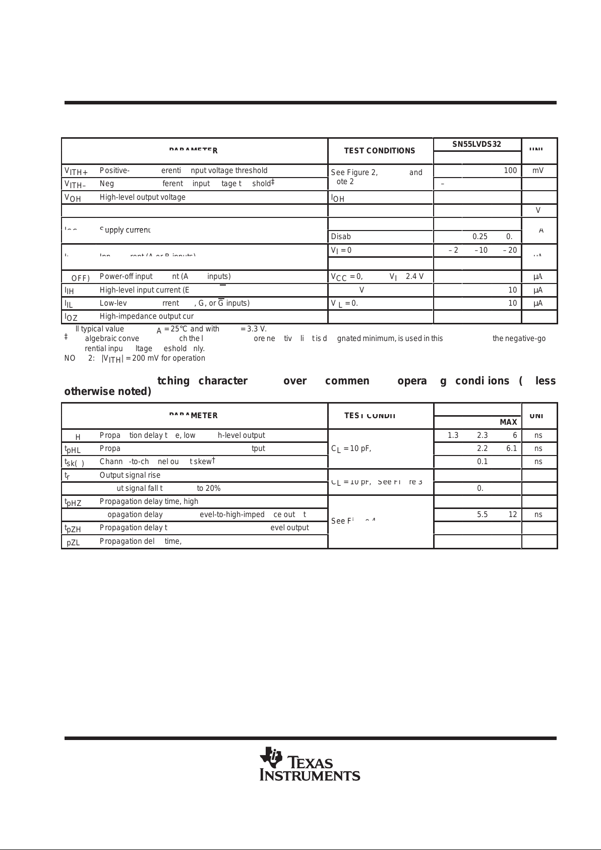
SN55LVDS32 Selectrical characteristics over recommended operating conditions (unless
otherwise noted)
ББББББББББББББББББ
SN55LVDS32
ББББББББББББББББББ
PARAMETER
TEST CONDITIONS
MIN
TYP†MAX
UNIT
ÁÁÁ
V
ITH+
Positive-going differential input voltage threshold
See Figure 2, Table 1, and
100
mV
ÁÁÁ
V
ITH–
Negative-going differential input voltage threshold
‡
g, ,
Note 2
–100
mV
ÁÁÁ
V
OH
High-level output voltage
IOH = –8 mA
2.4
V
ÁÁÁ
V
OL
Low-level output voltage
IOL = 8 mA
0.4
V
pp
Enabled, No load
10
18
ÁÁÁ
ICCSupply current
Disabled
0.25
0.5
mA
ÁÁÁ
p
p
VI = 0
–2
–10
–20
ÁÁÁ
IIInput current (A or B inputs)
VI = 2.4 V
–1.2
–3
µ
A
ÁÁÁ
I
I(OFF)
Power-off input current (A or B inputs)
VCC = 0, VI = 2.4 V
6
20
µA
ÁÁÁ
I
IH
High-level input current (EN, G, or G inputs)
VIH = 2 V
10
µA
ÁÁÁ
I
IL
Low-level input current (EN, G, or G inputs)
VIL = 0.8 V
10
µA
ÁÁÁ
I
OZ
High-impedance output current
VO = 0 or V
CC
±12
µA
†
All typical values are at TA = 25°C and with VCC = 3.3 V.
‡
The algebraic convention, in which the less positive (more negative) limit is designated minimum, is used in this data sheet for the negative-going
differential input voltage threshold only.
NOTE 2: |V
ITH
| = 200 mV for operation at –55°C.
SN55LVDS32 switching characteristics over recommended operating conditions (unless
otherwise noted)
ББББББББББББББББББ
SN55LVDS32
ББББББББББББББББББ
PARAMETER
TEST CONDITIONS
MIN
TYP
MAX
UNIT
t
pLH
Propagation delay time, low-to-high-level output
1.3
2.3
6
ns
ÁÁÁ
t
pHL
Propagation delay time, high-to-low-level output
CL = 10 pF, See Figure 3
1.4
2.2
6.1
ns
ÁÁÁ
t
sk(o)
Channel-to-channel output skew
†
0.1
ns
ÁÁÁ
t
r
Output signal rise time, 20% to 80%
p
0.6
ns
ÁÁÁ
t
f
Output signal fall time, 80% to 20%
C
L
= 10 pF,
See Figure 3
0.7
ns
ÁÁÁ
t
pHZ
Propagation delay time, high-level-to-high-impedance output
6.5
12
ns
ÁÁÁ
t
pLZ
Propagation delay time, low-level-to-high-impedance output
5.5
12
ns
ÁÁÁ
t
pZH
Propagation delay time, high-impedance-to-high-level output
See Figure 4
8
14
ns
ÁÁÁ
t
pZL
Propagation delay time, high-impedance-to-low-level output
3
12
ns
†
t
sk(o
) is the maximum delay time difference between drivers on the same device.
 Loading...