


Texas Instruments SN74ABT541BDBLE, SN74ABT541BDBR, SN74ABT541BDW, SN74ABT541BDWR, SN74ABT541BN Datasheet
...
|
|
|
|
|
|
SN54ABT541, SN74ABT541B |
|
|
|
|
|
|
|
OCTAL BUFFERS/DRIVERS |
|
|
|
|
|
|
|
WITH 3-STATE OUTPUTS |
|
|
|
|
|
|
|
SCBS093K ± JANUARY 1991 ± REVISED OCTOBER 1998 |
|
|
|
|
|
|
|
|
|
D |
State-of-the-Art EPIC- |
ΙΙ |
B |
|
BiCMOS Design |
SN54ABT541 . . . J OR W PACKAGE |
|
|
|
|
SN74ABT541B . . . DB, DW, N, OR PW PACKAGE |
||||
|
Significantly Reduces Power Dissipation |
||||||
|
|
|
|
|
|
(TOP VIEW) |
|
DLatch-Up Performance Exceeds 500 mA Per
JEDEC Standard JESD-17 |
|
|
|
|
|
|
|
|
|
|
OE1 |
|
1 |
20 |
|
|
VCC |
||||
D Typical VOLP (Output Ground Bounce) < 1 V |
|
A1 |
|
2 |
19 |
|
|
OE2 |
|
|
|
|
|
|
|
||||||
at VCC = 5 V, TA = 25°C |
|
A2 |
|
3 |
18 |
|
|
Y1 |
||
D High-Impedance State During Power Up |
|
A3 |
|
4 |
17 |
|
|
Y2 |
||
and Power Down |
|
A4 |
|
5 |
16 |
|
|
Y3 |
||
D High-Drive Outputs (±32-mA IOH, 64-mA IOL) |
|
A5 |
|
6 |
15 |
|
|
Y4 |
||
|
A6 |
|
7 |
14 |
|
|
Y5 |
|||
D Package Options Include Plastic |
|
|
|
|
||||||
|
A7 |
|
|
|
|
|
Y6 |
|||
|
|
8 |
13 |
|
|
|||||
Small-Outline (DW), Shrink Small-Outline |
|
|
|
|
||||||
|
A8 |
9 |
12 |
|
|
Y7 |
||||
(DB), and Thin Shrink Small-Outline (PW) |
|
|
|
|||||||
GND |
10 |
11 |
|
|
Y8 |
|||||
Packages, Ceramic Chip Carriers (FK), |
|
|
||||||||
Ceramic Flat (W) Package, and Plastic (N) |
|
|
|
|
|
|
|
|
|
|
and Ceramic (J) DIPs |
SN54ABT541 . . . FK PACKAGE |
|||||||||
|
|
|
|
|
(TOP VIEW) |
|
|
|||
description
The SN54ABT541 and SN74ABT541B octal buffers and line drivers are ideal for driving bus lines or buffering memory address registers. The devices feature inputs and outputs on opposite sides of the package to facilitate printed circuit board layout.
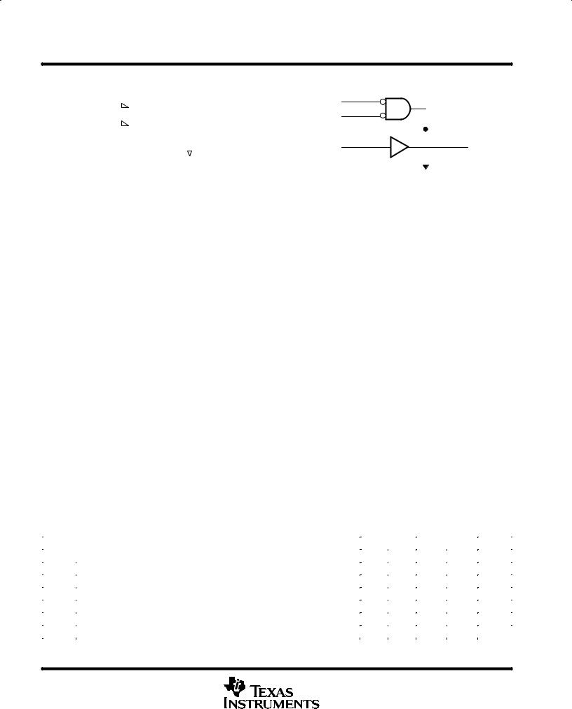
The 3-state control gate is a two-input AND gate with active-low inputs so that if either output-enable (OE1 or OE2) input is high, all eight outputs are in the high-impedance state.
|
A2 |
A1 |
OE1 |
CC |
OE2 |
|
|
V |
|
||||
A3 |
3 |
2 |
1 |
20 19 |
Y1 |
|
4 |
|
|
|
18 |
||
A4 |
5 |
|
|
|
17 |
Y2 |
A5 |
6 |
|
|
|
16 |
Y3 |
A6 |
7 |
|
|
|
15 |
Y4 |
A7 |
8 |
|
|
|
14 |
Y5 |
|
9 |
10 11 12 13 |
|
|||
|
A8 |
GND |
Y8 |
Y7 |
Y6 |
|
When VCC is between 0 and 2.1 V, the device is in the high-impedance state during power up or power down.
However, to ensure the high-impedance state above 2.1 V, OE should be tied to VCC through a pullup resistor; the minimum value of the resistor is determined by the current-sinking capability of the driver.
The SN54ABT541 is characterized for operation over the full military temperature range of ±55°C to 125°C. The SN74ABT541B is characterized for operation from ±40°C to 85°C.
FUNCTION TABLE
|
|
|
INPUTS |
|
OUTPUT |
||
|
|
|
|
|
|
A |
Y |
|
OE1 |
|
|
OE2 |
|
||
|
|
|
|
|
|
||
|
L |
|
L |
L |
L |
||
|
L |
|
L |
H |
H |
||
|
H |
|
X |
X |
Z |
||
|
X |
|
H |
X |
Z |
||
|
|
|
|
|
|
|
|
Please be aware that an important notice concerning availability, standard warranty, and use in critical applications of
Texas Instruments semiconductor products and disclaimers thereto appears at the end of this data sheet.
EPIC-ΙΙB is a trademark of Texas Instruments Incorporated.
PRODUCTION DATA information is current as of publication date. Products conform to specifications per the terms of Texas Instruments standard warranty. Production processing does not necessarily include testing of all parameters.
Copyright 1998, Texas Instruments Incorporated
On products compliant to MIL-PRF-38535, all parameters are tested unless otherwise noted. On all other products, production processing does not necessarily include testing of all parameters.
POST OFFICE BOX 655303 •DALLAS, TEXAS 75265 |
1 |
SN54ABT541, SN74ABT541B
OCTAL BUFFERS/DRIVERS
WITH 3-STATE OUTPUTS
SCBS093K ± JANUARY 1991 ± REVISED OCTOBER 1998
logic symbol² |
|
|
|
|
|
|
|
|
|
logic diagram (positive logic) |
|||||||||
|
|
|
|
|
|
|
|
|
|
|
|
|
|
|
|
1 |
|
|
|
|
|
1 |
& |
|
|
|
|
|
|
|
|
|
|
|
|
||||
|
|
|
|
|
|
|
|
OE1 |
|
|
|
||||||||
|
|
|
|
|
|
|
|
|
|
|
|
||||||||
OE1 |
|
|
|
|
|
EN |
|
|
|
|
|
19 |
|
|
|
||||
|
|
|
|
|
|
|
|
|
|
|
|
|
|||||||
|
|
19 |
|
|
|
|
|
|
|
|
|
OE2 |
|
|
|
||||
|
|
|
|
|
|
|
|
|
|
|
|
|
|
|
|||||
OE2 |
|
|
|
|
|
|
|
|
|
|
|
A1 |
2 |
|
|
18 |
|||
|
|
|
|
|
|
|
|
|
|
|
|
|
|||||||
|
|
|
|
|
|
|
|
|
|
|
|
|
|
|
|
||||
2 |
1 |
|
|
|
18 |
|
|
|
|
|
Y1 |
||||||||
|
A1 |
|
|
|
|
|
Y1 |
|
|
|
|
|
|
|
|||||
|
|
|
|
|
|
|
|
|
|
|
|
||||||||
3 |
|
|
|
|
|
17 |
|
|
|
|
|
|
|
|
|||||
|
|
|
|
|
|
|
|
|
|
|
|
|
|
|
|||||
|
A2 |
|
|
|
|
|
|
|
|
|
Y2 |
|
|
|
|
|
|
|
|
4 |
|
|
|
|
|
|
|
16 |
|
|
|
|
|
|
|
|
|||
|
|
|
|
|
|
|
|
|
|
|
|
|
|
|
|||||
|
A3 |
|
|
|
|
|
|
|
|
|
Y3 |
|
|
|
|
To Seven Other Channels |
|||
|
|
|
|
|
|
|
|
15 |
|
|
|
|
|||||||
5 |
|
|
|
|
|
|
|
Y4 |
|
|
|
|
|
|
|
||||
|
|
|
|
|
|
|
|
|
|
|
|
|
|
||||||
|
A4 |
|
|
|
|
|
|
|
|
|
|
|
|
|
|
|
|
||
|
|
|
|
|
|
|
|
|
|
|
|
|
|
|
|
||||
6 |
|
|
|
|
|
|
|
14 |
|
|
|
|
|
|
|
|
|||
|
|
|
|
|
|
|
|
|
|
|
|
|
|
|
|||||
|
A5 |
|
|
|
|
|
|
|
|
|
Y5 |
|
|
|
|
|
|
|
|
|
|
|
|
|
|
|
|
|
|
|
|
|
|
|
|
||||
7 |
|
|
|
|
|
|
|
13 |
|
|
|
|
|
|
|
|
|||
|
|
|
|
|
|
|
|
|
|
|
|
|
|
|
|||||
|
A6 |
|
|
|
|
|
|
|
|
|
Y6 |
|
|
|
|
|
|
|
|
|
|
|
|
|
|
|
|
|
|
|
|
|
|
|
|
||||
8 |
|
|
|
|
|
|
|
12 |
|
|
|
|
|
|
|
|
|||
|
|
|
|
|
|
|
|
|
|
|
|
|
|
|
|||||
|
A7 |
|
|
|
|
|
|
|
|
|
Y7 |
|
|
|
|
|
|
|
|
|
|
|
|
|
|
|
|
|
|
|
|
|
|
|
|
||||
9 |
|
|
|
|
|
|
|
11 |
|
|
|
|
|
|
|
|
|||
|
|
|
|
|
|
|
|
|
|
|
|
|
|
|
|||||
|
A8 |
|
|
|
|
|
|
|
|
|
Y8 |
|
|
|
|
|
|
|
|
|
|
|
|
|
|
|
|
|
|
|
|
|
|
|
|
||||
²This symbol is in accordance with ANSI/IEEE Std 91-1984 and
IEC Publication 617-12.
absolute maximum ratings over operating free-air temperature range (unless otherwise noted)³
Supply voltage range, VCC . . . . . . . . . . . . . . . . . . . . . . . . . . . . . . . . . . . . . . . . . . . . . . . . . . . . . . . . . |
. ±0.5 V to 7 |
V |
Input voltage range, VI (see Note 1) . . . . . . . . . . . . . . . . . . . . . . . . . . . . . . . . . . . . . . . . . . . . . . . . . |
. ±0.5 V to 7 |
V |
Voltage range applied to any output in the high or power-off state, VO . . . . . . . . . . . . . . . . . . . |
±0.5 V to 5.5 |
V |
Current into any output in the low state, IO: SN54ABT541 . . . . . . . . . . . . . . . . . . . . . . . . . . . . . |
. . . . . . . 96 mA |
|
SN74ABT541B . . . . . . . . . . . . . . . . . . . . . . . . . . . . |
. . . . . . 128 mA |
|
Input clamp current, IIK (VI < 0) . . . . . . . . . . . . . . . . . . . . . . . . . . . . . . . . . . . . . . . . . . . . . . . . . . . . . |
. . . . . . ±18 mA |
|
Output clamp current, IOK (VO < 0) . . . . . . . . . . . . . . . . . . . . . . . . . . . . . . . . . . . . . . . . . . . . . . . . . . |
. . . . . . ±50 mA |
|
Package thermal impedance, θJA (see Note 2): DB package . . . . . . . . . . . . . . . . . . . . . . . . . . . |
. . . . . 115°C/W |
|
DW package . . . . . . . . . . . . . . . . . . . . . . . . . . . |
. . . . . . 97°C/W |
|
N package . . . . . . . . . . . . . . . . . . . . . . . . . . . . . |
. . . . . . 67°C/W |
|
PW package . . . . . . . . . . . . . . . . . . . . . . . . . . . |
. . . . . 128°C/W |
|
Storage temperature range, Tstg . . . . . . . . . . . . . . . . . . . . . . . . . . . . . . . . . . . . . . . . . . . . . . . . . . . |
±65°C to 150°C |
|
³Stresses beyond those listed under ªabsolute maximum ratingsº may cause permanent damage to the device. These are stress ratings only, and functional operation of the device at these or any other conditions beyond those indicated under ªrecommended operating conditionsº is not implied. Exposure to absolute-maximum-rated conditions for extended periods may affect device reliability.
NOTES: 1. The input and output negative-voltage ratings may be exceeded if the input and output clamp-current ratings are observed.
2.The package thermal impedance is calculated in accordance with JESD 51, except for through-hole packages, which use a trace length of zero.
recommended operating conditions (see Note 3)
|
|
SN54ABT541 |
SN74ABT541B |
UNIT |
||
|
|
|
|
|
|
|
|
|
MIN |
MAX |
MIN |
MAX |
|
|
|
|
||||
|
|
|
|
|
|
|
VCC |
Supply voltage |
4.5 |
5.5 |
4.5 |
5.5 |
V |
VIH |
High-level input voltage |
2 |
|
2 |
|
V |
VIL |
Low-level input voltage |
|
0.8 |
|
0.8 |
V |
IOH |
High-level output current |
|
±24 |
|
±32 |
mA |
IOL |
Low-level output current |
|
48 |
|
64 |
mA |
TA |
Operating free-air temperature |
±55 |
125 |
±40 |
85 |
°C |
NOTE 3: All unused inputs of the device must be held at VCC or GND to ensure proper device operation. Refer to the TI application report,
Implications of Slow or Floating CMOS Inputs, literature number SCBA004.
2 |
POST OFFICE BOX 655303 •DALLAS, TEXAS 75265 |
 Loading...