


Texas Instruments SN74ABT3614-15PCB, SN74ABT3614-15PQ, SN74ABT3614-20PCB, SN74ABT3614-20PQ, SN74ABT3614-30PCB Datasheet
...SN74ABT3614 64 ×36 ×2 CLOCKED BIDIRECTIONAL FIRST-IN, FIRST-OUT MEMORY
WITH BUS MATCHING AND BYTE SWAPPING
SCBS126H ± JUNE 1992 ± REVISED APRIL 2000
DFree-Running CLKA and CLKB Can Be Asynchronous or Coincident
DTwo Independent 64 × 36 Clocked FIFOs
Buffering Data in Opposite Directions
DMailbox-Bypass Register for Each FIFO
DDynamic Port-B Bus Sizing of 36 Bits (Long Word), 18 Bits (Word), and 9 Bits (Byte)
DSelection of Bigor Little-Endian Format for Word and Byte Bus Sizes
DThree Modes of Byte-Order Swapping on Port B
DProgrammable Almost-Full and Almost-Empty Flags
DMicroprocessor Interface Control Logic
description
DEFA, FFA, AEA, and AFA Flags Synchronized by CLKA
DEFB, FFB, AEB, and AFB Flags Synchronized by CLKB
DPassive Parity Checking on Each Port
DParity Generation Can Be Selected for Each Port
DLow-Power Advanced BiCMOS Technology
DSupports Clock Frequencies up to 67 MHz
DFast Access Times of 10 ns
DPackage Options Include 120-Pin Thin Quad Flat (PCB) and 132-Pin Quad Flat (PQ) Packages
The SN74ABT3614 is a high-speed, low-power BiCMOS bidirectional clocked FIFO memory. It supports clock frequencies up to 67 MHz and has read-access times as fast as 10 ns. Two independent 64 ×36 dual-port SRAM FIFOs in this device buffer data in opposite directions. Each FIFO has flags to indicate empty and full conditions and two programmable flags, almost full (AF) and almost empty (AE) to indicate when a selected number of words is stored in memory. FIFO data on port B can be input and output in 36-bit, 18-bit, and 9-bit formats, with a choice of bigor little-endian configurations. Three modes of byte-order swapping are possible with any bus-size selection. Communication between each port can bypass the FIFOs via two 36-bit mailbox registers. Each mailbox register has a flag to signal when new mail has been stored. Parity is checked passively on each port and can be ignored if not desired. Parity generation can be selected for data read from each port.
The SN74ABT3614 is a clocked FIFO, which means each port employs a synchronous interface. All data transfers through a port are gated to the low-to-high transition of a continuous (free-running) port clock by enable signals. The continuous clocks for each port are independent of one another and can be asynchronous or coincident. The enables for each port are arranged to provide a simple bidirectional interface between microprocessors and/or buses controlled by a synchronous interface.
The full flag and almost-full flag of a FIFO are two-stage synchronized to the port clock that writes data to its array. The empty flag and almost-empty flag of a FIFO are two-stage synchronized to the port clock that reads data from its array.
The SN74ABT3614 is characterized for operation from 0°C to 70°C.
For more information on this device family, see the following application reports:
•FIFO Mailbox-Bypass Registers: Using Bypass Registers to Initialize DMA Control
(literature number SCAA007)
•Advanced Bus-Matching/Byte-Swapping Features for Internetworking FIFO Applications (literature number SCAA014)
•Parity-Generate and Parity-Check Features for High-Bandwidth-Computing FIFO Applications
(literature number SCAA015)
•Internetworking the SN74ABT3614 (literature number SCAA015)
•Metastability Performance of Clocked FIFOs (literature number SCZA004)
Please be aware that an important notice concerning availability, standard warranty, and use in critical applications of Texas Instruments semiconductor products and disclaimers thereto appears at the end of this data sheet.
PRODUCTION DATA information is current as of publication date. Products conform to specifications per the terms of Texas Instruments standard warranty. Production processing does not necessarily include testing of all parameters.
Copyright 2000, Texas Instruments Incorporated
POST OFFICE BOX 655303 •DALLAS, TEXAS 75265 |
1 |

SN74ABT3614
64 ×36 ×2 CLOCKED BIDIRECTIONAL FIRST-IN, FIRST-OUT MEMORY
WITH BUS MATCHING AND BYTE SWAPPING
SCBS126H ± JUNE 1992 ± REVISED APRIL 2000
PCB PACKAGE (TOP VIEW)
|
|
|
|
|
A24 |
A25 |
A26 |
|
CC |
A27 |
A28 |
A29 |
GND |
A30 |
A31 |
A32 |
A33 |
A34 |
A35 |
GND |
B35 |
B34 |
B33 |
B32 |
B31 |
B30 GND |
B29 |
B28 |
B27 |
CC |
B26 |
B25 |
B24 |
B23 |
|
|
|
|
|||||||||||||||||||||||||||||||||||||
|
|
|
|
|
V |
V |
|
|
|
|
|||||||||||||||||||||||||||||||||||||||||||||||||||||||||||||||||
|
|
|
|
|
|
|
|
|
|
|
|
|
|
|
|
|
|
|
|
|
|
|
|
|
|
|
|
|
|
|
|
|
|
|
|
|
|
|
|
|
|
|
|
|
|
|
|
|
|
|
|
|
|
|
|
|
|
|
|
|
|
|
|
|
|
|
|
|
|
|
|
|
|
|
|
|
A23 |
|
1 |
120 |
|
119 |
|
118 |
|
117 |
|
116 |
|
115 |
|
114 |
|
113 |
|
112 |
|
111 |
|
110 |
|
109 |
|
108 |
|
107 |
|
106 |
|
105 |
|
104 |
|
103 |
|
102 |
101 |
100 |
99 |
98 |
97 |
96 |
95 |
94 |
93 |
92 |
91 |
|
B22 |
||||||||||||||||||||||
|
|
|
|
|
|
|
|
|
|
|
|
|
|
|
|
|
|
|
|
|
|
|
|
|
|
|
|
|
|
|
|
|
|
|
|
|
|
|
|
|
|
|
|
|
|
|
|
|
|
|
|
|
|
|
|
|
|
|
|
|
|
|
|
|
|
|
90 |
|
|||||||
|
|
|
|
|
|
|
|
|
|
|
|
|
|
|
|
|
|
|
|
|
|
|
|
|
|
|
|
|
|
|
|
|
|
|
|
|
|
|
|
|
|
|
|
|
|
|
|
|
|
|
|
|
|
|
|
|
|
|
|
|
|
|
|
|
|
|
|||||||||
|
A22 |
|
2 |
|
|
|
|
|
|
|
|
|
|
|
|
|
|
|
|
|
|
|
|
|
|
|
|
|
|
|
|
|
|
|
|
|
|
|
|
|
|
|
|
|
|
|
|
|
|
|
|
|
|
|
|
|
|
|
|
|
|
|
|
|
|
|
|
|
89 |
|
B21 |
||||
|
|
|
|
|
|
|
|
|
|
|
|
|
|
|
|
|
|
|
|
|
|
|
|
|
|
|
|
|
|
|
|
|
|
|
|
|
|
|
|
|
|
|
|
|
|
|
|
|
|
|
|
|
|
|
|
|
|
|
|
|
|
|
|
|
|
|
|||||||||
|
A21 |
|
3 |
|
|
|
|
|
|
|
|
|
|
|
|
|
|
|
|
|
|
|
|
|
|
|
|
|
|
|
|
|
|
|
|
|
|
|
|
|
|
|
|
|
|
|
|
|
|
|
|
|
|
|
|
|
|
|
|
|
|
|
|
|
|
|
|
|
88 |
|
GND |
||||
|
|
|
|
|
|
|
|
|
|
|
|
|
|
|
|
|
|
|
|
|
|
|
|
|
|
|
|
|
|
|
|
|
|
|
|
|
|
|
|
|
|
|
|
|
|
|
|
|
|
|
|
|
|
|
|
|
|
|
|
|
|
|
|
|
|
|
|||||||||
GND |
|
4 |
|
|
|
|
|
|
|
|
|
|
|
|
|
|
|
|
|
|
|
|
|
|
|
|
|
|
|
|
|
|
|
|
|
|
|
|
|
|
|
|
|
|
|
|
|
|
|
|
|
|
|
|
|
|
|
|
|
|
|
|
|
|
|
|
|
87 |
|
B20 |
|||||
|
|
|
|
|
|
|
|
|
|
|
|
|
|
|
|
|
|
|
|
|
|
|
|
|
|
|
|
|
|
|
|
|
|
|
|
|
|
|
|
|
|
|
|
|
|
|
|
|
|
|
|
|
|
|
|
|
|
|
|
|
|
|
|
|
|
|
|||||||||
|
A20 |
|
5 |
|
|
|
|
|
|
|
|
|
|
|
|
|
|
|
|
|
|
|
|
|
|
|
|
|
|
|
|
|
|
|
|
|
|
|
|
|
|
|
|
|
|
|
|
|
|
|
|
|
|
|
|
|
|
|
|
|
|
|
|
|
|
|
|
|
86 |
|
B19 |
||||
|
|
|
|
|
|
|
|
|
|
|
|
|
|
|
|
|
|
|
|
|
|
|
|
|
|
|
|
|
|
|
|
|
|
|
|
|
|
|
|
|
|
|
|
|
|
|
|
|
|
|
|
|
|
|
|
|
|
|
|
|
|
|
|
|
|
|
|||||||||
|
A19 |
|
6 |
|
|
|
|
|
|
|
|
|
|
|
|
|
|
|
|
|
|
|
|
|
|
|
|
|
|
|
|
|
|
|
|
|
|
|
|
|
|
|
|
|
|
|
|
|
|
|
|
|
|
|
|
|
|
|
|
|
|
|
|
|
|
|
|
|
85 |
|
B18 |
||||
|
|
|
|
|
|
|
|
|
|
|
|
|
|
|
|
|
|
|
|
|
|
|
|
|
|
|
|
|
|
|
|
|
|
|
|
|
|
|
|
|
|
|
|
|
|
|
|
|
|
|
|
|
|
|
|
|
|
|
|
|
|
|
|
|
|
|
|||||||||
|
A18 |
|
7 |
|
|
|
|
|
|
|
|
|
|
|
|
|
|
|
|
|
|
|
|
|
|
|
|
|
|
|
|
|
|
|
|
|
|
|
|
|
|
|
|
|
|
|
|
|
|
|
|
|
|
|
|
|
|
|
|
|
|
|
|
|
|
|
|
|
84 |
|
B17 |
||||
|
|
|
|
|
|
|
|
|
|
|
|
|
|
|
|
|
|
|
|
|
|
|
|
|
|
|
|
|
|
|
|
|
|
|
|
|
|
|
|
|
|
|
|
|
|
|
|
|
|
|
|
|
|
|
|
|
|
|
|
|
|
|
|
|
|
|
|||||||||
|
A17 |
|
8 |
|
|
|
|
|
|
|
|
|
|
|
|
|
|
|
|
|
|
|
|
|
|
|
|
|
|
|
|
|
|
|
|
|
|
|
|
|
|
|
|
|
|
|
|
|
|
|
|
|
|
|
|
|
|
|
|
|
|
|
|
|
|
|
|
|
83 |
|
B16 |
||||
|
|
|
|
|
|
|
|
|
|
|
|
|
|
|
|
|
|
|
|
|
|
|
|
|
|
|
|
|
|
|
|
|
|
|
|
|
|
|
|
|
|
|
|
|
|
|
|
|
|
|
|
|
|
|
|
|
|
|
|
|
|
|
|
|
|
|
|||||||||
|
A16 |
|
9 |
|
|
|
|
|
|
|
|
|
|
|
|
|
|
|
|
|
|
|
|
|
|
|
|
|
|
|
|
|
|
|
|
|
|
|
|
|
|
|
|
|
|
|
|
|
|
|
|
|
|
|
|
|
|
|
|
|
|
|
|
|
|
|
|
|
82 |
|
B15 |
||||
|
|
|
|
|
|
|
|
|
|
|
|
|
|
|
|
|
|
|
|
|
|
|
|
|
|
|
|
|
|
|
|
|
|
|
|
|
|
|
|
|
|
|
|
|
|
|
|
|
|
|
|
|
|
|
|
|
|
|
|
|
|
|
|
|
|
|
|||||||||
|
A15 |
|
10 |
|
|
|
|
|
|
|
|
|
|
|
|
|
|
|
|
|
|
|
|
|
|
|
|
|
|
|
|
|
|
|
|
|
|
|
|
|
|
|
|
|
|
|
|
|
|
|
|
|
|
|
|
|
|
|
|
|
|
|
|
|
|
|
|
|
81 |
|
B14 |
||||
|
|
|
|
|
|
|
|
|
|
|
|
|
|
|
|
|
|
|
|
|
|
|
|
|
|
|
|
|
|
|
|
|
|
|
|
|
|
|
|
|
|
|
|
|
|
|
|
|
|
|
|
|
|
|
|
|
|
|
|
|
|
|
|
|
|
|
|||||||||
|
A14 |
|
11 |
|
|
|
|
|
|
|
|
|
|
|
|
|
|
|
|
|
|
|
|
|
|
|
|
|
|
|
|
|
|
|
|
|
|
|
|
|
|
|
|
|
|
|
|
|
|
|
|
|
|
|
|
|
|
|
|
|
|
|
|
|
|
|
|
|
80 |
|
B13 |
||||
|
|
|
|
|
|
|
|
|
|
|
|
|
|
|
|
|
|
|
|
|
|
|
|
|
|
|
|
|
|
|
|
|
|
|
|
|
|
|
|
|
|
|
|
|
|
|
|
|
|
|
|
|
|
|
|
|
|
|
|
|
|
|
|
|
|
|
|||||||||
|
A13 |
|
12 |
|
|
|
|
|
|
|
|
|
|
|
|
|
|
|
|
|
|
|
|
|
|
|
|
|
|
|
|
|
|
|
|
|
|
|
|
|
|
|
|
|
|
|
|
|
|
|
|
|
|
|
|
|
|
|
|
|
|
|
|
|
|
|
|
|
79 |
|
B12 |
||||
|
|
|
|
|
|
|
|
|
|
|
|
|
|
|
|
|
|
|
|
|
|
|
|
|
|
|
|
|
|
|
|
|
|
|
|
|
|
|
|
|
|
|
|
|
|
|
|
|
|
|
|
|
|
|
|
|
|
|
|
|
|
|
|
|
|
|
|||||||||
|
A12 |
|
13 |
|
|
|
|
|
|
|
|
|
|
|
|
|
|
|
|
|
|
|
|
|
|
|
|
|
|
|
|
|
|
|
|
|
|
|
|
|
|
|
|
|
|
|
|
|
|
|
|
|
|
|
|
|
|
|
|
|
|
|
|
|
|
|
|
|
78 |
|
B11 |
||||
|
|
|
|
|
|
|
|
|
|
|
|
|
|
|
|
|
|
|
|
|
|
|
|
|
|
|
|
|
|
|
|
|
|
|
|
|
|
|
|
|
|
|
|
|
|
|
|
|
|
|
|
|
|
|
|
|
|
|
|
|
|
|
|
|
|
|
|||||||||
|
A11 |
|
14 |
|
|
|
|
|
|
|
|
|
|
|
|
|
|
|
|
|
|
|
|
|
|
|
|
|
|
|
|
|
|
|
|
|
|
|
|
|
|
|
|
|
|
|
|
|
|
|
|
|
|
|
|
|
|
|
|
|
|
|
|
|
|
|
|
|
77 |
|
B10 |
||||
|
|
|
|
|
|
|
|
|
|
|
|
|
|
|
|
|
|
|
|
|
|
|
|
|
|
|
|
|
|
|
|
|
|
|
|
|
|
|
|
|
|
|
|
|
|
|
|
|
|
|
|
|
|
|
|
|
|
|
|
|
|
|
|
|
|
|
|||||||||
|
A10 |
|
15 |
|
|
|
|
|
|
|
|
|
|
|
|
|
|
|
|
|
|
|
|
|
|
|
|
|
|
|
|
|
|
|
|
|
|
|
|
|
|
|
|
|
|
|
|
|
|
|
|
|
|
|
|
|
|
|
|
|
|
|
|
|
|
|
|
|
76 |
|
GND |
||||
|
|
|
|
|
|
|
|
|
|
|
|
|
|
|
|
|
|
|
|
|
|
|
|
|
|
|
|
|
|
|
|
|
|
|
|
|
|
|
|
|
|
|
|
|
|
|
|
|
|
|
|
|
|
|
|
|
|
|
|
|
|
|
|
|
|
|
|||||||||
GND |
|
16 |
|
|
|
|
|
|
|
|
|
|
|
|
|
|
|
|
|
|
|
|
|
|
|
|
|
|
|
|
|
|
|
|
|
|
|
|
|
|
|
|
|
|
|
|
|
|
|
|
|
|
|
|
|
|
|
|
|
|
|
|
|
|
|
|
|
75 |
|
B9 |
|||||
|
|
|
|
|
|
|
|
|
|
|
|
|
|
|
|
|
|
|
|
|
|
|
|
|
|
|
|
|
|
|
|
|
|
|
|
|
|
|
|
|
|
|
|
|
|
|
|
|
|
|
|
|
|
|
|
|
|
|
|
|
|
|
|
|
|
|
|||||||||
|
A9 |
|
17 |
|
|
|
|
|
|
|
|
|
|
|
|
|
|
|
|
|
|
|
|
|
|
|
|
|
|
|
|
|
|
|
|
|
|
|
|
|
|
|
|
|
|
|
|
|
|
|
|
|
|
|
|
|
|
|
|
|
|
|
|
|
|
|
|
|
74 |
|
B8 |
||||
|
|
|
|
|
|
|
|
|
|
|
|
|
|
|
|
|
|
|
|
|
|
|
|
|
|
|
|
|
|
|
|
|
|
|
|
|
|
|
|
|
|
|
|
|
|
|
|
|
|
|
|
|
|
|
|
|
|
|
|
|
|
|
|
|
|
|
|||||||||
|
A8 |
|
18 |
|
|
|
|
|
|
|
|
|
|
|
|
|
|
|
|
|
|
|
|
|
|
|
|
|
|
|
|
|
|
|
|
|
|
|
|
|
|
|
|
|
|
|
|
|
|
|
|
|
|
|
|
|
|
|
|
|
|
|
|
|
|
|
|
|
73 |
|
B7 |
||||
|
|
|
|
|
|
|
|
|
|
|
|
|
|
|
|
|
|
|
|
|
|
|
|
|
|
|
|
|
|
|
|
|
|
|
|
|
|
|
|
|
|
|
|
|
|
|
|
|
|
|
|
|
|
|
|
|
|
|
|
|
|
|
|
|
|
|
|||||||||
|
A7 |
|
19 |
|
|
|
|
|
|
|
|
|
|
|
|
|
|
|
|
|
|
|
|
|
|
|
|
|
|
|
|
|
|
|
|
|
|
|
|
|
|
|
|
|
|
|
|
|
|
|
|
|
|
|
|
|
|
|
|
|
|
|
|
|
|
|
|
|
72 |
|
VCC |
||||
|
|
|
|
|
|
|
|
|
|
|
|
|
|
|
|
|
|
|
|
|
|
|
|
|
|
|
|
|
|
|
|
|
|
|
|
|
|
|
|
|
|
|
|
|
|
|
|
|
|
|
|
|
|
|
|
|
|
|
|
|
|
|
|
|
|
|
|||||||||
VCC |
|
20 |
|
|
|
|
|
|
|
|
|
|
|
|
|
|
|
|
|
|
|
|
|
|
|
|
|
|
|
|
|
|
|
|
|
|
|
|
|
|
|
|
|
|
|
|
|
|
|
|
|
|
|
|
|
|
|
|
|
|
|
|
|
|
|
|
|
71 |
|
B6 |
|||||
|
|
|
|
|
|
|
|
|
|
|
|
|
|
|
|
|
|
|
|
|
|
|
|
|
|
|
|
|
|
|
|
|
|
|
|
|
|
|
|
|
|
|
|
|
|
|
|
|
|
|
|
|
|
|
|
|
|
|
|
|
|
|
|
|
|
|
|||||||||
|
A6 |
|
21 |
|
|
|
|
|
|
|
|
|
|
|
|
|
|
|
|
|
|
|
|
|
|
|
|
|
|
|
|
|
|
|
|
|
|
|
|
|
|
|
|
|
|
|
|
|
|
|
|
|
|
|
|
|
|
|
|
|
|
|
|
|
|
|
|
|
70 |
|
B5 |
||||
|
|
|
|
|
|
|
|
|
|
|
|
|
|
|
|
|
|
|
|
|
|
|
|
|
|
|
|
|
|
|
|
|
|
|
|
|
|
|
|
|
|
|
|
|
|
|
|
|
|
|
|
|
|
|
|
|
|
|
|
|
|
|
|
|
|
|
|||||||||
|
A5 |
|
22 |
|
|
|
|
|
|
|
|
|
|
|
|
|
|
|
|
|
|
|
|
|
|
|
|
|
|
|
|
|
|
|
|
|
|
|
|
|
|
|
|
|
|
|
|
|
|
|
|
|
|
|
|
|
|
|
|
|
|
|
|
|
|
|
|
|
69 |
|
B4 |
||||
|
|
|
|
|
|
|
|
|
|
|
|
|
|
|
|
|
|
|
|
|
|
|
|
|
|
|
|
|
|
|
|
|
|
|
|
|
|
|
|
|
|
|
|
|
|
|
|
|
|
|
|
|
|
|
|
|
|
|
|
|
|
|
|
|
|
|
|||||||||
|
A4 |
|
23 |
|
|
|
|
|
|
|
|
|
|
|
|
|
|
|
|
|
|
|
|
|
|
|
|
|
|
|
|
|
|
|
|
|
|
|
|
|
|
|
|
|
|
|
|
|
|
|
|
|
|
|
|
|
|
|
|
|
|
|
|
|
|
|
|
|
68 |
|
B3 |
||||
|
|
|
|
|
|
|
|
|
|
|
|
|
|
|
|
|
|
|
|
|
|
|
|
|
|
|
|
|
|
|
|
|
|
|
|
|
|
|
|
|
|
|
|
|
|
|
|
|
|
|
|
|
|
|
|
|
|
|
|
|
|
|
|
|
|
|
|||||||||
|
A3 |
|
24 |
|
|
|
|
|
|
|
|
|
|
|
|
|
|
|
|
|
|
|
|
|
|
|
|
|
|
|
|
|
|
|
|
|
|
|
|
|
|
|
|
|
|
|
|
|
|
|
|
|
|
|
|
|
|
|
|
|
|
|
|
|
|
|
|
|
67 |
|
GND |
||||
|
|
|
|
|
|
|
|
|
|
|
|
|
|
|
|
|
|
|
|
|
|
|
|
|
|
|
|
|
|
|
|
|
|
|
|
|
|
|
|
|
|
|
|
|
|
|
|
|
|
|
|
|
|
|
|
|
|
|
|
|
|
|
|
|
|
|
|||||||||
GND |
|
25 |
|
|
|
|
|
|
|
|
|
|
|
|
|
|
|
|
|
|
|
|
|
|
|
|
|
|
|
|
|
|
|
|
|
|
|
|
|
|
|
|
|
|
|
|
|
|
|
|
|
|
|
|
|
|
|
|
|
|
|
|
|
|
|
|
|
66 |
|
B2 |
|||||
|
|
|
|
|
|
|
|
|
|
|
|
|
|
|
|
|
|
|
|
|
|
|
|
|
|
|
|
|
|
|
|
|
|
|
|
|
|
|
|
|
|
|
|
|
|
|
|
|
|
|
|
|
|
|
|
|
|
|
|
|
|
|
|
|
|
|
|||||||||
|
A2 |
|
26 |
|
|
|
|
|
|
|
|
|
|
|
|
|
|
|
|
|
|
|
|
|
|
|
|
|
|
|
|
|
|
|
|
|
|
|
|
|
|
|
|
|
|
|
|
|
|
|
|
|
|
|
|
|
|
|
|
|
|
|
|
|
|
|
|
|
65 |
|
B1 |
||||
|
|
|
|
|
|
|
|
|
|
|
|
|
|
|
|
|
|
|
|
|
|
|
|
|
|
|
|
|
|
|
|
|
|
|
|
|
|
|
|
|
|
|
|
|
|
|
|
|
|
|
|
|
|
|
|
|
|
|
|
|
|
|
|
|
|
|
|||||||||
|
A1 |
|
27 |
|
|
|
|
|
|
|
|
|
|
|
|
|
|
|
|
|
|
|
|
|
|
|
|
|
|
|
|
|
|
|
|
|
|
|
|
|
|
|
|
|
|
|
|
|
|
|
|
|
|
|
|
|
|
|
|
|
|
|
|
|
|
|
|
|
64 |
|
B0 |
||||
|
|
|
|
|
|
|
|
|
|
|
|
|
|
|
|
|
|
|
|
|
|
|
|
|
|
|
|
|
|
|
|
|
|
|
|
|
|
|
|
|
|
|
|
|
|
|
|
|
|
|
|
|
|
|
|
|
|
|
|
|
|
|
|
|
|
|
|||||||||
|
|
|
|
28 |
|
|
|
|
|
|
|
|
|
|
|
|
|
|
|
|
|
|
|
|
|
|
|
|
|
|
|
|
|
|
|
|
|
|
|
|
|
|
|
|
|
|
|
|
|
|
|
|
|
|
|
|
|
|
|
|
|
|
|
|
|
|
|
|
|
63 |
|
|
|
|
|
|
A0 |
|
|
|
|
|
|
|
|
|
|
|
|
|
|
|
|
|
|
|
|
|
|
|
|
|
|
|
|
|
|
|
|
|
|
|
|
|
|
|
|
|
|
|
|
|
|
|
|
|
|
|
|
|
|
|
|
|
|
|
|
|
|
|
|
|
|
EFB |
|||||||
|
29 |
|
|
|
|
|
|
|
|
|
|
|
|
|
|
|
|
|
|
|
|
|
|
|
|
|
|
|
|
|
|
|
|
|
|
|
|
|
|
|
|
|
|
|
|
|
|
|
|
|
|
|
|
|
|
|
|
|
|
|
|
|
|
|
|
|
62 |
|
|||||||
|
|
|
|
|
|
|
|
|
|
|
|
|
|
|
|
|
|
|
|
|
|
|
|
|
|
|
|
|
|
|
|
|
|
|
|
|
|
|
|
|
|
|
|
|
|
|
|
|
|
|
|
|
|
|
|
|
|
|
|
|
|
|
|
|
|
|
|
|
|
AEB |
|||||
|
EFA |
|
|
|
|
|
|
|
|
|
|
|
|
|
|
|
|
|
|
|
|
|
|
|
|
|
|
|
|
|
|
|
|
|
|
|
|
|
|
|
|
|
|
|
|
|
|
|
|
|
|
|
|
|
|
|
|
|
|
|
|
|
|
|
|
|
|
||||||||
|
30 |
|
|
|
|
|
|
|
|
|
|
|
|
|
|
|
|
|
|
|
|
|
|
|
|
|
|
|
|
|
|
|
|
|
|
|
|
|
|
|
|
|
|
|
|
|
|
|
|
|
|
|
|
|
|
|
|
|
|
|
|
|
|
|
|
|
61 |
|
|||||||
AEA |
|
|
|
|
|
|
|
|
|
|
|
|
|
|
|
|
|
|
|
|
|
|
|
|
|
|
|
|
|
|
|
|
|
|
|
|
|
|
|
|
|
|
|
|
|
|
|
|
|
|
|
|
|
|
|
|
|
|
|
|
|
|
|
|
|
|
|
AFB |
|||||||
|
|
|
|
|
|
|
|
|
|
|
|
|
|
|
|
|
|
|
|
|
|
|
|
|
|
|
|
|
|
|
|
|
|
|
|
|
|
|
|
|
|
|
|
|
|
|
|
|
|
|
|
|
|
|
|
|
|
|
|
|
|
|
|
|
|
||||||||||
|
|
|
|
|
31 |
32 |
33 |
34 |
35 |
36 |
37 |
38 |
39 |
40 |
41 |
42 |
43 |
44 |
45 |
46 |
47 |
48 |
49 |
50 |
51 |
52 |
53 |
54 |
55 |
56 |
57 |
58 |
59 |
60 |
|
|
|
|
|
||||||||||||||||||||||||||||||||||||
|
|
|
|
|
|
|
|
|
|
|
|
|
|
|
|
|
|
|
|
|
|
|
|
|
|
|
|
|
|
|
|
|
|
|
|
|
|
|
|
|
|
|
|
|
|
|
|
|
|
|
|
|
|
|
|
|
|
|
|
|
|
|
|
|
|
|
|
|
|
|
|
|
|
||
|
|
|
|
|
|
|
|
|
|
|
|
|
|
|
|
|
|
|
|
|
|
|
|
|
|
|
|
|
|
|
|
|
|
|
|
|
|
|
|
|
|
|
|
|
|
|
|
|
|
|
|
|
|
|
|
|
|
|
|
|
|
|
|
|
|
|
|
|
|
|
|
|
|
||
|
|
|
|
|
AFA |
FFA |
CSA |
|
ENA |
CLKA |
W/RA |
V |
PGA PEFA MBF2 |
MBA FS1 |
|
FS0 |
ODD/EVEN |
RST GND |
BE SW1 |
|
SW0 |
SIZ1 |
SIZ0 |
MBF1 |
PEFB |
|
PGB V |
W/RB |
CLKB |
ENB |
CSB |
FFB |
|
|
|
|
|||||||||||||||||||||||||||||||||||||||
|
|
|
|
|
|
|
|
|
|
|
|
|
|
|
|
|
|
|
CC |
|
|
|
|
|
|
|
|
|
|
|
|
|
|
|
|
|
|
|
|
|
|
|
|
|
|
|
|
|
|
|
|
|
|
|
|
|
|
|
CC |
|
|
|
|
|
|
|
|
|
|
|
|
|
|
||
|
|
|
|
|
|
|
|
|
|
|
|
|
|
|
|
|
|
|
|
|
|
|
|
|
|
|
|
|
|
|
|
|
|
|
|
|
|
|
|
|
|
|
|
|
|
|
|
|
|
|
|
|
|
|
|
|
|
|
|
|
|
|
|
|
|
|
|
|
|
|
|
||||
|
|
|
|
|
|
|
|
|
|
|
|
|
|
|
|
|
|
|
|
|
|
|
|
|
|
|
|
|
|
|
|
|
|
|
|
|
|
|
|
|
|
|
|
|
|
|
|
|
|
|
|
|
|
|
|
|
|
|
|
|
|
|
|
|
|
|
|
|
|
|
|
|
|
|
|
|
|
|
|
|
|
|
|
|
|
|
|
|
|
|
|
|
|
|
|
|
|
|
|
|
|
|
|
|
|
|
|
|
|
|
|
|
|
|
|
|
|
|
|
|
|
|
|
|
|
|
|
|
|
|
|
|
|
|
|
|
|
|
|
|
|
|
|
|
|
|
|
|
|
|
|
|
|
|
|
|
|
|
|
|
|
|
|
|
|
|
|
|
|
|
|
|
|
|
|
|
|
|
|
|
|
|
|
|
|
|
|
|
|
|
|
|
|
|
|
|
|
|
|
|
|
|
|
|
|
|
|
|
|
|
|
|
|
|
|
|
|
|
|
|
|
|
|
|
|
|
|
2 |
POST OFFICE BOX 655303 •DALLAS, TEXAS 75265 |
SN74ABT3614 64 ×36 ×2 CLOCKED BIDIRECTIONAL FIRST-IN, FIRST-OUT MEMORY
WITH BUS MATCHING AND BYTE SWAPPING
SCBS126H ± JUNE 1992 ± REVISED APRIL 2000
PQ PACKAGE² (TOP VIEW)
|
|
|
|
|
AFA |
FFA |
CSA |
ENA |
CLKA |
W/RA |
V |
PGA |
PEFA |
GND |
MBF2 |
MBA |
FS1 |
FS0 |
|
ODD/EVEN |
RST |
GND |
BE |
SW1 |
SW0 |
SIZ1 |
SIZ0 |
MBF1 |
GND |
PEFB |
|
PGB |
V |
|
W/RB |
CLKB |
ENB |
CSB |
|
FFB |
|
AFB |
|||||||||||||||||||||||||||||||||||||||||||||||||
|
|
|
|
|
|
|
|
|
|
|
|
|
|
|
|
|
|
CC |
|
|
|
|
|
|
|
|
|
|
|
|
|
|
|
|
|
|
|
|
|
|
|
|
|
|
|
|
|
|
|
|
|
|
|
|
|
|
|
|
|
|
|
|
|
|
|
|
|
|
|
CC |
|
|
|
|
|
|
|
|
|
|
|
|
|
|
|
|
|
|
|
||
|
|
|
|
|
|
|
|
|
|
|
|
|
|
|
|
|
|
|
|
|
|
|
|
|
|
|
|
|
|
|
|
|
|
|
|
|
|
|
|
|
|
|
|
|
|
|
|
|
|
|
|
|
|
|
|
|
|
|
|
|
|
|
|
|
|
|
|
|
|
|
|
|
|
|
|
|
|
|
|
|
|
|
|
|
|
|
|
||||
|
|
|
|
|
|
|
|
|
|
|
|
|
|
|
|
|
|
|
|
|
|
|
|
|
|
|
|
|
|
|
|
|
|
|
|
|
|
|
|
|
|
|
|
|
|
|
|
|
|
|
|
|
|
|
|
|
|
|
|
|
|
|
|
|
|
|
|
|
|
|
|
|
|
|
|
|
|
|
|
|
|
|
|
|
|
|
|
|
|
|
|
|
|
|
|
|
|
|
|
|
|
|
|
|
|
|
|
|
|
|
|
|
|
|
|
|
|
|
|
|
|
|
|
|
|
|
|
|
|
|
|
|
|
|
|
|
|
|
|
|
|
|
|
|
|
|
|
|
|
|
|
|
|
|
|
|
|
|
|
|
|
|
|
|
|
|
|
|
|
|
|
|
|
|
|
|
|
|
|
|
|
|
|
|
|
|
|
|
|
|
|
|
|
|
|
|
|
|
|
|
|
|
|
|
|
|
|
|
|
|
|
|
|
|
|
|
|
|
|
|
|
|
|
|
|
|
|
|
|
|
|
|
|
|
|
|
|
|
|
|
|
|
|
|
|
|
|
|
|
|
|
|
|
|
|
|
|
|
|
|
|
|
|
|
|
|
|
|
|
|
|
|
|
|
|
|
|
|
17 16 15 14 13 12 11 10 |
9 |
|
8 |
|
7 |
|
6 |
|
5 |
|
4 |
3 |
|
2 |
|
1 132 |
130 |
|
|
128 |
|
|
|
126 |
|
|
|
124 |
|
|
|
122 |
|
|
|
120 |
|
|
118 |
|
|
|
|
|||||||||||||||||||||||||||||||||||||||||||||
GND |
|
|
18 |
|
|
|
|
|
|
|
|
|
|
|
|
|
|
|
|
|
|
|
|
|
|
|
|
|
|
|
|
|
|
|
|
|
|
|
|
|
|
|
|
|
|
131 |
129 |
|
|
127 |
|
|
125 |
|
|
123 |
|
|
121 |
|
|
119 |
|
|
|
117 |
|
||||||||||||||||||||||||
|
|
|
|
|
|
|
|
|
|
|
|
|
|
|
|
|
|
|
|
|
|
|
|
|
|
|
|
|
|
|
|
|
|
|
|
|
|
|
|
|
|
|
|
|
|
|
|
|
|
|
|
|
|
|
|
|
|
|
|
|
|
|
|
|
|
|
|
|
|
|
|
|
|
|
|
|
|
|
|
|
|
|
|
|
116 |
||||||
|
|
|
|
|
|
|
|
|
|
|
|
|
|
|
|
|
|
|
|
|
|
|
|
|
|
|
|
|
|
|
|
|
|
|
|
|
|
|
|
|
|
|
|
|
|
|
|
|
|
|
|
|
|
|
|
|
|
|
|
|
|
|
|
|
|
|
|
|
|
|
|
|
|
|
|
|
|
|
|
|
|
||||||||||
AEA |
|
|
19 |
|
|
|
|
|
|
|
|
|
|
|
|
|
|
|
|
|
|
|
|
|
|
|
|
|
|
|
|
|
|
|
|
|
|
|
|
|
|
|
|
|
|
|
|
|
|
|
|
|
|
|
|
|
|
|
|
|
|
|
|
|
|
|
|
|
|
|
|
|
|
|
|
|
|
|
|
|
|
|
|
|
|
|
115 |
||||
|
|
|
|
|
|
|
|
|
|
|
|
|
|
|
|
|
|
|
|
|
|
|
|
|
|
|
|
|
|
|
|
|
|
|
|
|
|
|
|
|
|
|
|
|
|
|
|
|
|
|
|
|
|
|
|
|
|
|
|
|
|
|
|
|
|
|
|
|
|
|
|
|
|
|
|
|
|
|
|
|
|
||||||||||
|
|
|
|
|
|
|
|
|
|
|
|
|
|
|
|
|
|
|
|
|
|
|
|
|
|
|
|
|
|
|
|
|
|
|
|
|
|
|
|
|
|
|
|
|
|
|
|
|
|
|
|
|
|
|
|
|
|
|
|
|
|
|
|
|
|
|
|
|
|
|
|
|
|
|
|
|
|
|
|
|
|
||||||||||
EFA |
|
|
20 |
|
|
|
|
|
|
|
|
|
|
|
|
|
|
|
|
|
|
|
|
|
|
|
|
|
|
|
|
|
|
|
|
|
|
|
|
|
|
|
|
|
|
|
|
|
|
|
|
|
|
|
|
|
|
|
|
|
|
|
|
|
|
|
|
|
|
|
|
|
|
|
|
|
|
|
|
|
|
|
|
|
|
|
114 |
||||
|
|
|
|
|
|
|
|
|
|
|
|
|
|
|
|
|
|
|
|
|
|
|
|
|
|
|
|
|
|
|
|
|
|
|
|
|
|
|
|
|
|
|
|
|
|
|
|
|
|
|
|
|
|
|
|
|
|
|
|
|
|
|
|
|
|
|
|
|
|
|
|
|
|
|
|
|
|
|
|
|
|
||||||||||
|
|
|
|
|
|
|
|
|
|
|
|
|
|
|
|
|
|
|
|
|
|
|
|
|
|
|
|
|
|
|
|
|
|
|
|
|
|
|
|
|
|
|
|
|
|
|
|
|
|
|
|
|
|
|
|
|
|
|
|
|
|
|
|
|
|
|
|
|
|
|
|
|
|
|
|
|
|
|
|
|
|
||||||||||
A0 |
|
|
21 |
|
|
|
|
|
|
|
|
|
|
|
|
|
|
|
|
|
|
|
|
|
|
|
|
|
|
|
|
|
|
|
|
|
|
|
|
|
|
|
|
|
|
|
|
|
|
|
|
|
|
|
|
|
|
|
|
|
|
|
|
|
|
|
|
|
|
|
|
|
|
|
|
|
|
|
|
|
|
|
|
|
|
|
113 |
||||
|
|
|
|
|
|
|
|
|
|
|
|
|
|
|
|
|
|
|
|
|
|
|
|
|
|
|
|
|
|
|
|
|
|
|
|
|
|
|
|
|
|
|
|
|
|
|
|
|
|
|
|
|
|
|
|
|
|
|
|
|
|
|
|
|
|
|
|
|
|
|
|
|
|
|
|
|
|
|
|
|
|
||||||||||
|
|
|
|
|
|
|
|
|
|
|
|
|
|
|
|
|
|
|
|
|
|
|
|
|
|
|
|
|
|
|
|
|
|
|
|
|
|
|
|
|
|
|
|
|
|
|
|
|
|
|
|
|
|
|
|
|
|
|
|
|
|
|
|
|
|
|
|
|
|
|
|
|
|
|
|
|
|
|
|
|
|
||||||||||
A1 |
|
|
22 |
|
|
|
|
|
|
|
|
|
|
|
|
|
|
|
|
|
|
|
|
|
|
|
|
|
|
|
|
|
|
|
|
|
|
|
|
|
|
|
|
|
|
|
|
|
|
|
|
|
|
|
|
|
|
|
|
|
|
|
|
|
|
|
|
|
|
|
|
|
|
|
|
|
|
|
|
|
|
|
|
|
|
|
112 |
||||
|
|
|
|
|
|
|
|
|
|
|
|
|
|
|
|
|
|
|
|
|
|
|
|
|
|
|
|
|
|
|
|
|
|
|
|
|
|
|
|
|
|
|
|
|
|
|
|
|
|
|
|
|
|
|
|
|
|
|
|
|
|
|
|
|
|
|
|
|
|
|
|
|
|
|
|
|
|
|
|
|
|
||||||||||
|
|
|
|
|
|
|
|
|
|
|
|
|
|
|
|
|
|
|
|
|
|
|
|
|
|
|
|
|
|
|
|
|
|
|
|
|
|
|
|
|
|
|
|
|
|
|
|
|
|
|
|
|
|
|
|
|
|
|
|
|
|
|
|
|
|
|
|
|
|
|
|
|
|
|
|
|
|
|
|
|
|
||||||||||
A2 |
|
|
23 |
|
|
|
|
|
|
|
|
|
|
|
|
|
|
|
|
|
|
|
|
|
|
|
|
|
|
|
|
|
|
|
|
|
|
|
|
|
|
|
|
|
|
|
|
|
|
|
|
|
|
|
|
|
|
|
|
|
|
|
|
|
|
|
|
|
|
|
|
|
|
|
|
|
|
|
|
|
|
|
|
|
|
|
111 |
||||
|
|
|
|
|
|
|
|
|
|
|
|
|
|
|
|
|
|
|
|
|
|
|
|
|
|
|
|
|
|
|
|
|
|
|
|
|
|
|
|
|
|
|
|
|
|
|
|
|
|
|
|
|
|
|
|
|
|
|
|
|
|
|
|
|
|
|
|
|
|
|
|
|
|
|
|
|
|
|
|
|
|
||||||||||
|
|
|
|
|
|
|
|
|
|
|
|
|
|
|
|
|
|
|
|
|
|
|
|
|
|
|
|
|
|
|
|
|
|
|
|
|
|
|
|
|
|
|
|
|
|
|
|
|
|
|
|
|
|
|
|
|
|
|
|
|
|
|
|
|
|
|
|
|
|
|
|
|
|
|
|
|
|
|
|
|
|
||||||||||
GND |
|
|
24 |
|
|
|
|
|
|
|
|
|
|
|
|
|
|
|
|
|
|
|
|
|
|
|
|
|
|
|
|
|
|
|
|
|
|
|
|
|
|
|
|
|
|
|
|
|
|
|
|
|
|
|
|
|
|
|
|
|
|
|
|
|
|
|
|
|
|
|
|
|
|
|
|
|
|
|
|
|
|
|
|
|
|
|
110 |
||||
|
|
|
|
|
|
|
|
|
|
|
|
|
|
|
|
|
|
|
|
|
|
|
|
|
|
|
|
|
|
|
|
|
|
|
|
|
|
|
|
|
|
|
|
|
|
|
|
|
|
|
|
|
|
|
|
|
|
|
|
|
|
|
|
|
|
|
|
|
|
|
|
|
|
|
|
|
|
|
|
|
|
||||||||||
|
|
|
|
|
|
|
|
|
|
|
|
|
|
|
|
|
|
|
|
|
|
|
|
|
|
|
|
|
|
|
|
|
|
|
|
|
|
|
|
|
|
|
|
|
|
|
|
|
|
|
|
|
|
|
|
|
|
|
|
|
|
|
|
|
|
|
|
|
|
|
|
|
|
|
|
|
|
|
|
|
|
||||||||||
A3 |
|
|
25 |
|
|
|
|
|
|
|
|
|
|
|
|
|
|
|
|
|
|
|
|
|
|
|
|
|
|
|
|
|
|
|
|
|
|
|
|
|
|
|
|
|
|
|
|
|
|
|
|
|
|
|
|
|
|
|
|
|
|
|
|
|
|
|
|
|
|
|
|
|
|
|
|
|
|
|
|
|
|
|
|
|
|
|
109 |
||||
|
|
|
|
|
|
|
|
|
|
|
|
|
|
|
|
|
|
|
|
|
|
|
|
|
|
|
|
|
|
|
|
|
|
|
|
|
|
|
|
|
|
|
|
|
|
|
|
|
|
|
|
|
|
|
|
|
|
|
|
|
|
|
|
|
|
|
|
|
|
|
|
|
|
|
|
|
|
|
|
|
|
||||||||||
|
|
|
|
|
|
|
|
|
|
|
|
|
|
|
|
|
|
|
|
|
|
|
|
|
|
|
|
|
|
|
|
|
|
|
|
|
|
|
|
|
|
|
|
|
|
|
|
|
|
|
|
|
|
|
|
|
|
|
|
|
|
|
|
|
|
|
|
|
|
|
|
|
|
|
|
|
|
|
|
|
|
||||||||||
A4 |
|
|
26 |
|
|
|
|
|
|
|
|
|
|
|
|
|
|
|
|
|
|
|
|
|
|
|
|
|
|
|
|
|
|
|
|
|
|
|
|
|
|
|
|
|
|
|
|
|
|
|
|
|
|
|
|
|
|
|
|
|
|
|
|
|
|
|
|
|
|
|
|
|
|
|
|
|
|
|
|
|
|
|
|
|
|
|
108 |
||||
|
|
|
|
|
|
|
|
|
|
|
|
|
|
|
|
|
|
|
|
|
|
|
|
|
|
|
|
|
|
|
|
|
|
|
|
|
|
|
|
|
|
|
|
|
|
|
|
|
|
|
|
|
|
|
|
|
|
|
|
|
|
|
|
|
|
|
|
|
|
|
|
|
|
|
|
|
|
|
|
|
|
||||||||||
|
|
|
|
|
|
|
|
|
|
|
|
|
|
|
|
|
|
|
|
|
|
|
|
|
|
|
|
|
|
|
|
|
|
|
|
|
|
|
|
|
|
|
|
|
|
|
|
|
|
|
|
|
|
|
|
|
|
|
|
|
|
|
|
|
|
|
|
|
|
|
|
|
|
|
|
|
|
|
|
|
|
||||||||||
A5 |
|
|
27 |
|
|
|
|
|
|
|
|
|
|
|
|
|
|
|
|
|
|
|
|
|
|
|
|
|
|
|
|
|
|
|
|
|
|
|
|
|
|
|
|
|
|
|
|
|
|
|
|
|
|
|
|
|
|
|
|
|
|
|
|
|
|
|
|
|
|
|
|
|
|
|
|
|
|
|
|
|
|
|
|
|
|
|
107 |
||||
|
|
|
|
|
|
|
|
|
|
|
|
|
|
|
|
|
|
|
|
|
|
|
|
|
|
|
|
|
|
|
|
|
|
|
|
|
|
|
|
|
|
|
|
|
|
|
|
|
|
|
|
|
|
|
|
|
|
|
|
|
|
|
|
|
|
|
|
|
|
|
|
|
|
|
|
|
|
|
|
|
|
||||||||||
|
|
|
|
|
|
|
|
|
|
|
|
|
|
|
|
|
|
|
|
|
|
|
|
|
|
|
|
|
|
|
|
|
|
|
|
|
|
|
|
|
|
|
|
|
|
|
|
|
|
|
|
|
|
|
|
|
|
|
|
|
|
|
|
|
|
|
|
|
|
|
|
|
|
|
|
|
|
|
|
|
|
||||||||||
A6 |
|
|
28 |
|
|
|
|
|
|
|
|
|
|
|
|
|
|
|
|
|
|
|
|
|
|
|
|
|
|
|
|
|
|
|
|
|
|
|
|
|
|
|
|
|
|
|
|
|
|
|
|
|
|
|
|
|
|
|
|
|
|
|
|
|
|
|
|
|
|
|
|
|
|
|
|
|
|
|
|
|
|
|
|
|
|
|
106 |
||||
|
|
|
|
|
|
|
|
|
|
|
|
|
|
|
|
|
|
|
|
|
|
|
|
|
|
|
|
|
|
|
|
|
|
|
|
|
|
|
|
|
|
|
|
|
|
|
|
|
|
|
|
|
|
|
|
|
|
|
|
|
|
|
|
|
|
|
|
|
|
|
|
|
|
|
|
|
|
|
|
|
|
||||||||||
|
|
|
|
|
|
|
|
|
|
|
|
|
|
|
|
|
|
|
|
|
|
|
|
|
|
|
|
|
|
|
|
|
|
|
|
|
|
|
|
|
|
|
|
|
|
|
|
|
|
|
|
|
|
|
|
|
|
|
|
|
|
|
|
|
|
|
|
|
|
|
|
|
|
|
|
|
|
|
|
|
|
||||||||||
VCC |
|
|
29 |
|
|
|
|
|
|
|
|
|
|
|
|
|
|
|
|
|
|
|
|
|
|
|
|
|
|
|
|
|
|
|
|
|
|
|
|
|
|
|
|
|
|
|
|
|
|
|
|
|
|
|
|
|
|
|
|
|
|
|
|
|
|
|
|
|
|
|
|
|
|
|
|
|
|
|
|
|
|
|
|
|
|
|
105 |
||||
|
|
|
|
|
|
|
|
|
|
|
|
|
|
|
|
|
|
|
|
|
|
|
|
|
|
|
|
|
|
|
|
|
|
|
|
|
|
|
|
|
|
|
|
|
|
|
|
|
|
|
|
|
|
|
|
|
|
|
|
|
|
|
|
|
|
|
|
|
|
|
|
|
|
|
|
|
|
|
|
|
|
||||||||||
|
|
|
|
|
|
|
|
|
|
|
|
|
|
|
|
|
|
|
|
|
|
|
|
|
|
|
|
|
|
|
|
|
|
|
|
|
|
|
|
|
|
|
|
|
|
|
|
|
|
|
|
|
|
|
|
|
|
|
|
|
|
|
|
|
|
|
|
|
|
|
|
|
|
|
|
|
|
|
|
|
|
||||||||||
A7 |
|
|
30 |
|
|
|
|
|
|
|
|
|
|
|
|
|
|
|
|
|
|
|
|
|
|
|
|
|
|
|
|
|
|
|
|
|
|
|
|
|
|
|
|
|
|
|
|
|
|
|
|
|
|
|
|
|
|
|
|
|
|
|
|
|
|
|
|
|
|
|
|
|
|
|
|
|
|
|
|
|
|
|
|
|
|
|
104 |
||||
|
|
|
|
|
|
|
|
|
|
|
|
|
|
|
|
|
|
|
|
|
|
|
|
|
|
|
|
|
|
|
|
|
|
|
|
|
|
|
|
|
|
|
|
|
|
|
|
|
|
|
|
|
|
|
|
|
|
|
|
|
|
|
|
|
|
|
|
|
|
|
|
|
|
|
|
|
|
|
|
|
|
|
|
|
|||||||
|
|
|
|
|
|
|
|
|
|
|
|
|
|
|
|
|
|
|
|
|
|
|
|
|
|
|
|
|
|
|
|
|
|
|
|
|
|
|
|
|
|
|
|
|
|
|
|
|
|
|
|
|
|
|
|
|
|
|
|
|
|
|
|
|
|
|
|
|
|
|
|
|
|
|
|
|
|
|
|
|
|
||||||||||
A8 |
|
|
31 |
|
|
|
|
|
|
|
|
|
|
|
|
|
|
|
|
|
|
|
|
|
|
|
|
|
|
|
|
|
|
|
|
|
|
|
|
|
|
|
|
|
|
|
|
|
|
|
|
|
|
|
|
|
|
|
|
|
|
|
|
|
|
|
|
|
|
|
|
|
|
|
|
|
|
|
|
|
|
|
|
|
|
|
103 |
||||
|
|
|
|
|
|
|
|
|
|
|
|
|
|
|
|
|
|
|
|
|
|
|
|
|
|
|
|
|
|
|
|
|
|
|
|
|
|
|
|
|
|
|
|
|
|
|
|
|
|
|
|
|
|
|
|
|
|
|
|
|
|
|
|
|
|
|
|
|
|
|
|
|
|
|
|
|
|
|
|
|
|
||||||||||
|
|
|
|
|
|
|
|
|
|
|
|
|
|
|
|
|
|
|
|
|
|
|
|
|
|
|
|
|
|
|
|
|
|
|
|
|
|
|
|
|
|
|
|
|
|
|
|
|
|
|
|
|
|
|
|
|
|
|
|
|
|
|
|
|
|
|
|
|
|
|
|
|
|
|
|
|
|
|
|
|
|
||||||||||
A9 |
|
|
32 |
|
|
|
|
|
|
|
|
|
|
|
|
|
|
|
|
|
|
|
|
|
|
|
|
|
|
|
|
|
|
|
|
|
|
|
|
|
|
|
|
|
|
|
|
|
|
|
|
|
|
|
|
|
|
|
|
|
|
|
|
|
|
|
|
|
|
|
|
|
|
|
|
|
|
|
|
|
|
|
|
|
|
|
102 |
||||
|
|
|
|
|
|
|
|
|
|
|
|
|
|
|
|
|
|
|
|
|
|
|
|
|
|
|
|
|
|
|
|
|
|
|
|
|
|
|
|
|
|
|
|
|
|
|
|
|
|
|
|
|
|
|
|
|
|
|
|
|
|
|
|
|
|
|
|
|
|
|
|
|
|
|
|
|
|
|
|
|
|
||||||||||
|
|
|
|
|
|
|
|
|
|
|
|
|
|
|
|
|
|
|
|
|
|
|
|
|
|
|
|
|
|
|
|
|
|
|
|
|
|
|
|
|
|
|
|
|
|
|
|
|
|
|
|
|
|
|
|
|
|
|
|
|
|
|
|
|
|
|
|
|
|
|
|
|
|
|
|
|
|
|
|
|
|
||||||||||
GND |
|
|
33 |
|
|
|
|
|
|
|
|
|
|
|
|
|
|
|
|
|
|
|
|
|
|
|
|
|
|
|
|
|
|
|
|
|
|
|
|
|
|
|
|
|
|
|
|
|
|
|
|
|
|
|
|
|
|
|
|
|
|
|
|
|
|
|
|
|
|
|
|
|
|
|
|
|
|
|
|
|
|
|
|
|
|
|
101 |
||||
|
|
|
|
|
|
|
|
|
|
|
|
|
|
|
|
|
|
|
|
|
|
|
|
|
|
|
|
|
|
|
|
|
|
|
|
|
|
|
|
|
|
|
|
|
|
|
|
|
|
|
|
|
|
|
|
|
|
|
|
|
|
|
|
|
|
|
|
|
|
|
|
|
|
|
|
|
|
|
|
|
|
||||||||||
|
|
|
|
|
|
|
|
|
|
|
|
|
|
|
|
|
|
|
|
|
|
|
|
|
|
|
|
|
|
|
|
|
|
|
|
|
|
|
|
|
|
|
|
|
|
|
|
|
|
|
|
|
|
|
|
|
|
|
|
|
|
|
|
|
|
|
|
|
|
|
|
|
|
|
|
|
|
|
|
|
|
||||||||||
A10 |
|
|
34 |
|
|
|
|
|
|
|
|
|
|
|
|
|
|
|
|
|
|
|
|
|
|
|
|
|
|
|
|
|
|
|
|
|
|
|
|
|
|
|
|
|
|
|
|
|
|
|
|
|
|
|
|
|
|
|
|
|
|
|
|
|
|
|
|
|
|
|
|
|
|
|
|
|
|
|
|
|
|
|
|
|
|
|
100 |
||||
|
|
|
|
|
|
|
|
|
|
|
|
|
|
|
|
|
|
|
|
|
|
|
|
|
|
|
|
|
|
|
|
|
|
|
|
|
|
|
|
|
|
|
|
|
|
|
|
|
|
|
|
|
|
|
|
|
|
|
|
|
|
|
|
|
|
|
|
|
|
|
|
|
|
|
|
|
|
|
|
|
|
||||||||||
|
|
|
|
|
|
|
|
|
|
|
|
|
|
|
|
|
|
|
|
|
|
|
|
|
|
|
|
|
|
|
|
|
|
|
|
|
|
|
|
|
|
|
|
|
|
|
|
|
|
|
|
|
|
|
|
|
|
|
|
|
|
|
|
|
|
|
|
|
|
|
|
|
|
|
|
|
|
|
|
|
|
||||||||||
A11 |
|
|
35 |
|
|
|
|
|
|
|
|
|
|
|
|
|
|
|
|
|
|
|
|
|
|
|
|
|
|
|
|
|
|
|
|
|
|
|
|
|
|
|
|
|
|
|
|
|
|
|
|
|
|
|
|
|
|
|
|
|
|
|
|
|
|
|
|
|
|
|
|
|
|
|
|
|
|
|
|
|
|
|
|
|
|
|
99 |
||||
|
|
|
|
|
|
|
|
|
|
|
|
|
|
|
|
|
|
|
|
|
|
|
|
|
|
|
|
|
|
|
|
|
|
|
|
|
|
|
|
|
|
|
|
|
|
|
|
|
|
|
|
|
|
|
|
|
|
|
|
|
|
|
|
|
|
|
|
|
|
|
|
|
|
|
|
|
|
|
|
|
|
||||||||||
|
|
|
|
|
|
|
|
|
|
|
|
|
|
|
|
|
|
|
|
|
|
|
|
|
|
|
|
|
|
|
|
|
|
|
|
|
|
|
|
|
|
|
|
|
|
|
|
|
|
|
|
|
|
|
|
|
|
|
|
|
|
|
|
|
|
|
|
|
|
|
|
|
|
|
|
|
|
|
|
|
|
||||||||||
VCC |
|
|
36 |
|
|
|
|
|
|
|
|
|
|
|
|
|
|
|
|
|
|
|
|
|
|
|
|
|
|
|
|
|
|
|
|
|
|
|
|
|
|
|
|
|
|
|
|
|
|
|
|
|
|
|
|
|
|
|
|
|
|
|
|
|
|
|
|
|
|
|
|
|
|
|
|
|
|
|
|
|
|
|
|
|
|
|
98 |
||||
|
|
|
|
|
|
|
|
|
|
|
|
|
|
|
|
|
|
|
|
|
|
|
|
|
|
|
|
|
|
|
|
|
|
|
|
|
|
|
|
|
|
|
|
|
|
|
|
|
|
|
|
|
|
|
|
|
|
|
|
|
|
|
|
|
|
|
|
|
|
|
|
|
|
|
|
|
|
|
|
|
|
||||||||||
|
|
|
|
|
|
|
|
|
|
|
|
|
|
|
|
|
|
|
|
|
|
|
|
|
|
|
|
|
|
|
|
|
|
|
|
|
|
|
|
|
|
|
|
|
|
|
|
|
|
|
|
|
|
|
|
|
|
|
|
|
|
|
|
|
|
|
|
|
|
|
|
|
|
|
|
|
|
|
|
|
|
||||||||||
A12 |
|
|
37 |
|
|
|
|
|
|
|
|
|
|
|
|
|
|
|
|
|
|
|
|
|
|
|
|
|
|
|
|
|
|
|
|
|
|
|
|
|
|
|
|
|
|
|
|
|
|
|
|
|
|
|
|
|
|
|
|
|
|
|
|
|
|
|
|
|
|
|
|
|
|
|
|
|
|
|
|
|
|
|
|
|
|
|
97 |
||||
|
|
|
|
|
|
|
|
|
|
|
|
|
|
|
|
|
|
|
|
|
|
|
|
|
|
|
|
|
|
|
|
|
|
|
|
|
|
|
|
|
|
|
|
|
|
|
|
|
|
|
|
|
|
|
|
|
|
|
|
|
|
|
|
|
|
|
|
|
|
|
|
|
|
|
|
|
|
|
|
|
|
||||||||||
|
|
|
|
|
|
|
|
|
|
|
|
|
|
|
|
|
|
|
|
|
|
|
|
|
|
|
|
|
|
|
|
|
|
|
|
|
|
|
|
|
|
|
|
|
|
|
|
|
|
|
|
|
|
|
|
|
|
|
|
|
|
|
|
|
|
|
|
|
|
|
|
|
|
|
|
|
|
|
|
|
|
||||||||||
A13 |
|
|
38 |
|
|
|
|
|
|
|
|
|
|
|
|
|
|
|
|
|
|
|
|
|
|
|
|
|
|
|
|
|
|
|
|
|
|
|
|
|
|
|
|
|
|
|
|
|
|
|
|
|
|
|
|
|
|
|
|
|
|
|
|
|
|
|
|
|
|
|
|
|
|
|
|
|
|
|
|
|
|
|
|
|
|
|
96 |
||||
|
|
|
|
|
|
|
|
|
|
|
|
|
|
|
|
|
|
|
|
|
|
|
|
|
|
|
|
|
|
|
|
|
|
|
|
|
|
|
|
|
|
|
|
|
|
|
|
|
|
|
|
|
|
|
|
|
|
|
|
|
|
|
|
|
|
|
|
|
|
|
|
|
|
|
|
|
|
|
|
|
|
||||||||||
|
|
|
|
|
|
|
|
|
|
|
|
|
|
|
|
|
|
|
|
|
|
|
|
|
|
|
|
|
|
|
|
|
|
|
|
|
|
|
|
|
|
|
|
|
|
|
|
|
|
|
|
|
|
|
|
|
|
|
|
|
|
|
|
|
|
|
|
|
|
|
|
|
|
|
|
|
|
|
|
|
|
||||||||||
A14 |
|
|
39 |
|
|
|
|
|
|
|
|
|
|
|
|
|
|
|
|
|
|
|
|
|
|
|
|
|
|
|
|
|
|
|
|
|
|
|
|
|
|
|
|
|
|
|
|
|
|
|
|
|
|
|
|
|
|
|
|
|
|
|
|
|
|
|
|
|
|
|
|
|
|
|
|
|
|
|
|
|
|
|
|
|
|
|
95 |
||||
|
|
|
|
|
|
|
|
|
|
|
|
|
|
|
|
|
|
|
|
|
|
|
|
|
|
|
|
|
|
|
|
|
|
|
|
|
|
|
|
|
|
|
|
|
|
|
|
|
|
|
|
|
|
|
|
|
|
|
|
|
|
|
|
|
|
|
|
|
|
|
|
|
|
|
|
|
|
|
|
|
|
||||||||||
|
|
|
|
|
|
|
|
|
|
|
|
|
|
|
|
|
|
|
|
|
|
|
|
|
|
|
|
|
|
|
|
|
|
|
|
|
|
|
|
|
|
|
|
|
|
|
|
|
|
|
|
|
|
|
|
|
|
|
|
|
|
|
|
|
|
|
|
|
|
|
|
|
|
|
|
|
|
|
|
|
|
||||||||||
GND |
|
|
40 |
|
|
|
|
|
|
|
|
|
|
|
|
|
|
|
|
|
|
|
|
|
|
|
|
|
|
|
|
|
|
|
|
|
|
|
|
|
|
|
|
|
|
|
|
|
|
|
|
|
|
|
|
|
|
|
|
|
|
|
|
|
|
|
|
|
|
|
|
|
|
|
|
|
|
|
|
|
|
|
|
|
|
|
94 |
||||
|
|
|
|
|
|
|
|
|
|
|
|
|
|
|
|
|
|
|
|
|
|
|
|
|
|
|
|
|
|
|
|
|
|
|
|
|
|
|
|
|
|
|
|
|
|
|
|
|
|
|
|
|
|
|
|
|
|
|
|
|
|
|
|
|
|
|
|
|
|
|
|
|
|
|
|
|
|
|
|
|
|
||||||||||
|
|
|
|
|
|
|
|
|
|
|
|
|
|
|
|
|
|
|
|
|
|
|
|
|
|
|
|
|
|
|
|
|
|
|
|
|
|
|
|
|
|
|
|
|
|
|
|
|
|
|
|
|
|
|
|
|
|
|
|
|
|
|
|
|
|
|
|
|
|
|
|
|
|
|
|
|
|
|
|
|
|
||||||||||
A15 |
|
|
41 |
|
|
|
|
|
|
|
|
|
|
|
|
|
|
|
|
|
|
|
|
|
|
|
|
|
|
|
|
|
|
|
|
|
|
|
|
|
|
|
|
|
|
|
|
|
|
|
|
|
|
|
|
|
|
|
|
|
|
|
|
|
|
|
|
|
|
|
|
|
|
|
|
|
|
|
|
|
|
|
|
|
|
|
93 |
||||
|
|
|
|
|
|
|
|
|
|
|
|
|
|
|
|
|
|
|
|
|
|
|
|
|
|
|
|
|
|
|
|
|
|
|
|
|
|
|
|
|
|
|
|
|
|
|
|
|
|
|
|
|
|
|
|
|
|
|
|
|
|
|
|
|
|
|
|
|
|
|
|
|
|
|
|
|
|
|
|
|
|
||||||||||
|
|
|
|
|
|
|
|
|
|
|
|
|
|
|
|
|
|
|
|
|
|
|
|
|
|
|
|
|
|
|
|
|
|
|
|
|
|
|
|
|
|
|
|
|
|
|
|
|
|
|
|
|
|
|
|
|
|
|
|
|
|
|
|
|
|
|
|
|
|
|
|
|
|
|
|
|
|
|
|
|
|
||||||||||
A16 |
|
|
42 |
|
|
|
|
|
|
|
|
|
|
|
|
|
|
|
|
|
|
|
|
|
|
|
|
|
|
|
|
|
|
|
|
|
|
|
|
|
|
|
|
|
|
|
|
|
|
|
|
|
|
|
|
|
|
|
|
|
|
|
|
|
|
|
|
|
|
|
|
|
|
|
|
|
|
|
|
|
|
|
|
|
|
|
92 |
||||
|
|
|
|
|
|
|
|
|
|
|
|
|
|
|
|
|
|
|
|
|
|
|
|
|
|
|
|
|
|
|
|
|
|
|
|
|
|
|
|
|
|
|
|
|
|
|
|
|
|
|
|
|
|
|
|
|
|
|
|
|
|
|
|
|
|
|
|
|
|
|
|
|
|
|
|
|
|
|
|
|
|
||||||||||
|
|
|
|
|
|
|
|
|
|
|
|
|
|
|
|
|
|
|
|
|
|
|
|
|
|
|
|
|
|
|
|
|
|
|
|
|
|
|
|
|
|
|
|
|
|
|
|
|
|
|
|
|
|
|
|
|
|
|
|
|
|
|
|
|
|
|
|
|
|
|
|
|
|
|
|
|
|
|
|
|
|
||||||||||
A17 |
|
|
43 |
|
|
|
|
|
|
|
|
|
|
|
|
|
|
|
|
|
|
|
|
|
|
|
|
|
|
|
|
|
|
|
|
|
|
|
|
|
|
|
|
|
|
|
|
|
|
|
|
|
|
|
|
|
|
|
|
|
|
|
|
|
|
|
|
|
|
|
|
|
|
|
|
|
|
|
|
|
|
|
|
|
|
|
91 |
||||
|
|
|
|
|
|
|
|
|
|
|
|
|
|
|
|
|
|
|
|
|
|
|
|
|
|
|
|
|
|
|
|
|
|
|
|
|
|
|
|
|
|
|
|
|
|
|
|
|
|
|
|
|
|
|
|
|
|
|
|
|
|
|
|
|
|
|
|
|
|
|
|
|
|
|
|
|
|
|
|
|
|
||||||||||
|
|
|
|
|
|
|
|
|
|
|
|
|
|
|
|
|
|
|
|
|
|
|
|
|
|
|
|
|
|
|
|
|
|
|
|
|
|
|
|
|
|
|
|
|
|
|
|
|
|
|
|
|
|
|
|
|
|
|
|
|
|
|
|
|
|
|
|
|
|
|
|
|
|
|
|
|
|
|
|
|
|
||||||||||
A18 |
|
|
44 |
|
|
|
|
|
|
|
|
|
|
|
|
|
|
|
|
|
|
|
|
|
|
|
|
|
|
|
|
|
|
|
|
|
|
|
|
|
|
|
|
|
|
|
|
|
|
|
|
|
|
|
|
|
|
|
|
|
|
|
|
|
|
|
|
|
|
|
|
|
|
|
|
|
|
|
|
|
|
|
|
|
|
|
90 |
||||
|
|
|
|
|
|
|
|
|
|
|
|
|
|
|
|
|
|
|
|
|
|
|
|
|
|
|
|
|
|
|
|
|
|
|
|
|
|
|
|
|
|
|
|
|
|
|
|
|
|
|
|
|
|
|
|
|
|
|
|
|
|
|
|
|
|
|
|
|
|
|
|
|
|
|
|
|
|
|
|
|
|
||||||||||
|
|
|
|
|
|
|
|
|
|
|
|
|
|
|
|
|
|
|
|
|
|
|
|
|
|
|
|
|
|
|
|
|
|
|
|
|
|
|
|
|
|
|
|
|
|
|
|
|
|
|
|
|
|
|
|
|
|
|
|
|
|
|
|
|
|
|
|
|
|
|
|
|
|
|
|
|
|
|
|
|
|
||||||||||
A19 |
|
|
45 |
|
|
|
|
|
|
|
|
|
|
|
|
|
|
|
|
|
|
|
|
|
|
|
|
|
|
|
|
|
|
|
|
|
|
|
|
|
|
|
|
|
|
|
|
|
|
|
|
|
|
|
|
|
|
|
|
|
|
|
|
|
|
|
|
|
|
|
|
|
|
|
|
|
|
|
|
|
|
|
|
|
|
|
89 |
||||
|
|
|
|
|
|
|
|
|
|
|
|
|
|
|
|
|
|
|
|
|
|
|
|
|
|
|
|
|
|
|
|
|
|
|
|
|
|
|
|
|
|
|
|
|
|
|
|
|
|
|
|
|
|
|
|
|
|
|
|
|
|
|
|
|
|
|
|
|
|
|
|
|
|
|
|
|
|
|
|
|
|
||||||||||
|
|
|
|
|
|
|
|
|
|
|
|
|
|
|
|
|
|
|
|
|
|
|
|
|
|
|
|
|
|
|
|
|
|
|
|
|
|
|
|
|
|
|
|
|
|
|
|
|
|
|
|
|
|
|
|
|
|
|
|
|
|
|
|
|
|
|
|
|
|
|
|
|
|
|
|
|
|
|
|
|
|
||||||||||
A20 |
|
|
46 |
|
|
|
|
|
|
|
|
|
|
|
|
|
|
|
|
|
|
|
|
|
|
|
|
|
|
|
|
|
|
|
|
|
|
|
|
|
|
|
|
|
|
|
|
|
|
|
|
|
|
|
|
|
|
|
|
|
|
|
|
|
|
|
|
|
|
|
|
|
|
|
|
|
|
|
|
|
|
|
|
|
|
|
88 |
||||
|
|
|
|
|
|
|
|
|
|
|
|
|
|
|
|
|
|
|
|
|
|
|
|
|
|
|
|
|
|
|
|
|
|
|
|
|
|
|
|
|
|
|
|
|
|
|
|
|
|
|
|
|
|
|
|
|
|
|
|
|
|
|
|
|
|
|
|
|
|
|
|
|
|
|
|
|
|
|
|
|
|
||||||||||
|
|
|
|
|
|
|
|
|
|
|
|
|
|
|
|
|
|
|
|
|
|
|
|
|
|
|
|
|
|
|
|
|
|
|
|
|
|
|
|
|
|
|
|
|
|
|
|
|
|
|
|
|
|
|
|
|
|
|
|
|
|
|
|
|
|
|
|
|
|
|
|
|
|
|
|
|
|
|
|
|
|
||||||||||
GND |
|
|
47 |
|
|
|
|
|
|
|
|
|
|
|
|
|
|
|
|
|
|
|
|
|
|
|
|
|
|
|
|
|
|
|
|
|
|
|
|
|
|
|
|
|
|
|
|
|
|
|
|
|
|
|
|
|
|
|
|
|
|
|
|
|
|
|
|
|
|
|
|
|
|
|
|
|
|
|
|
|
|
|
|
|
|
|
87 |
||||
|
|
|
|
|
|
|
|
|
|
|
|
|
|
|
|
|
|
|
|
|
|
|
|
|
|
|
|
|
|
|
|
|
|
|
|
|
|
|
|
|
|
|
|
|
|
|
|
|
|
|
|
|
|
|
|
|
|
|
|
|
|
|
|
|
|
|
|
|
|
|
|
|
|
|
|
|
|
|
|
|
|
||||||||||
|
|
|
|
|
|
|
|
|
|
|
|
|
|
|
|
|
|
|
|
|
|
|
|
|
|
|
|
|
|
|
|
|
|
|
|
|
|
|
|
|
|
|
|
|
|
|
|
|
|
|
|
|
|
|
|
|
|
|
|
|
|
|
|
|
|
|
|
|
|
|
|
|
|
|
|
|
|
|
|
|
|
||||||||||
A21 |
|
|
48 |
|
|
|
|
|
|
|
|
|
|
|
|
|
|
|
|
|
|
|
|
|
|
|
|
|
|
|
|
|
|
|
|
|
|
|
|
|
|
|
|
|
|
|
|
|
|
|
|
|
|
|
|
|
|
|
|
|
|
|
|
|
|
|
|
|
|
|
|
|
|
|
|
|
|
|
|
|
|
|
|
|
|
|
86 |
||||
|
|
|
|
|
|
|
|
|
|
|
|
|
|
|
|
|
|
|
|
|
|
|
|
|
|
|
|
|
|
|
|
|
|
|
|
|
|
|
|
|
|
|
|
|
|
|
|
|
|
|
|
|
|
|
|
|
|
|
|
|
|
|
|
|
|
|
|
|
|
|
|
|
|
|
|
|
|
|
|
|
|
||||||||||
|
|
|
|
|
|
|
|
|
|
|
|
|
|
|
|
|
|
|
|
|
|
|
|
|
|
|
|
|
|
|
|
|
|
|
|
|
|
|
|
|
|
|
|
|
|
|
|
|
|
|
|
|
|
|
|
|
|
|
|
|
|
|
|
|
|
|
|
|
|
|
|
|
|
|
|
|
|
|
|
|
|
||||||||||
A22 |
|
|
49 |
|
|
|
|
|
|
|
|
|
|
|
|
|
|
|
|
|
|
|
|
|
|
|
|
|
|
|
|
|
|
|
|
|
|
|
|
|
|
|
|
|
|
|
|
|
|
|
|
|
|
|
|
|
|
|
|
|
|
|
|
|
|
|
|
|
|
|
|
|
|
|
|
|
|
|
|
|
|
|
|
|
|
|
85 |
||||
|
|
|
|
|
|
|
|
|
|
|
|
|
|
|
|
|
|
|
|
|
|
|
|
|
|
|
|
|
|
|
|
|
|
|
|
|
|
|
|
|
|
|
|
|
|
|
|
|
|
|
|
|
|
|
|
|
|
|
|
|
|
|
|
|
|
|
|
|
|
|
|
|
|
|
|
|
|
|
|
|
|
||||||||||
|
|
|
|
|
|
|
|
|
|
|
|
|
|
|
|
|
|
|
|
|
|
|
|
|
|
|
|
|
|
|
|
|
|
|
|
|
|
|
|
|
|
|
|
|
|
|
|
|
|
|
|
|
|
|
|
|
|
|
|
|
|
|
|
|
|
|
|
|
|
|
|
|
|
|
|
|
|
|
|
|
|
||||||||||
A23 |
|
|
50 |
|
|
|
|
|
|
|
|
|
|
|
|
|
|
|
|
|
|
|
|
|
|
|
|
|
|
|
|
|
|
|
|
|
|
|
|
|
|
|
|
|
|
|
|
|
|
|
|
|
|
|
|
|
|
|
|
|
|
|
|
|
|
|
|
|
|
|
|
|
|
|
|
|
|
|
|
|
|
|
|
|
|
|
84 |
||||
|
|
|
|
|
|
|
|
|
|
|
|
|
|
|
|
|
|
|
|
|
|
|
|
|
|
|
|
|
|
|
|
|
|
|
|
|
|
|
|
|
|
|
|
|
|
|
|
|
|
|
|
|
|
|
|
|
|
|
|
|
|
|
|
|
|
|
|
|
|
|
|
|
|
|
|
|
|
|
|
|
|
||||||||||
|
|
|
|
|
|
|
|
|
|
|
|
|
|
|
|
|
|
|
|
|
|
|
|
|
|
|
|
|
|
|
|
|
|
|
|
|
|
|
|
|
|
|
|
|
|
|
|
|
|
|
|
|
|
|
|
|
|
|
|
|
|
|
|
|
|
|
|
|
|
|
|
|
|
|
|
|
|
|
|
|
|
||||||||||
|
|
|
51 52 53 54 55 56 57 58 59 60 61 62 63 64 65 66 67 68 69 70 71 72 73 74 75 76 77 78 79 80 81 82 83 |
|
|||||||||||||||||||||||||||||||||||||||||||||||||||||||||||||||||||||||||||||||||||||||
|
|
||||||||||||||||||||||||||||||||||||||||||||||||||||||||||||||||||||||||||||||||||||||||||
|
|
|
|
|
|
|
|
|
|
|
|
|
|
|
|
|
|
|
|
|
|
|
|
|
|
|
|
|
|
|
|
|
|
|
|
|
|
|
|
|
|
|
|
|
|
|
|
|
|
|
|
|
|
|
|
|
|
|
|
|
|
|
|
|
|
|
|
|
|
|
|
|
|
|
|
|
|
|
|
|
|
|
|
|
|
|
|
|
|
|
|
|
|
|
|
|
|
|
|
|
|
|
|
|
|
|
|
|
|
|
|
|
|
|
|
|
|
|
|
|
|
|
|
|
|
|
|
|
|
|
|
|
|
|
|
|
|
|
|
|
|
|
|
|
|
|
|
|
|
|
|
|
|
|
|
|
|
|
|
|
|
|
|
|
|
|
|
|
|
|
|
|
|
|
|
|
|
|
|
|
|
|
|
|
|
|
|
|
|
CC |
A24 |
A25 |
A26 |
GND |
A27 |
A28 |
A29 |
CC |
A30 |
A31 |
A32 |
GND |
A33 |
|
A34 |
A35 |
GND |
B35 |
B34 |
B33 |
GND |
|
B32 |
B31 |
B30 |
|
CC |
B29 |
|
B28 |
|
B27 |
GND |
B26 |
B25 |
|
B24 |
|
CC |
||||||||||||||||||||||||||||||||||||||||||||||
|
|
|
|
|
V |
V |
|
|
V |
|
|
|
|
V |
|||||||||||||||||||||||||||||||||||||||||||||||||||||||||||||||||||||||||||||
NC ± No internal connection
² Uses Yamaichi socket IC51-1324-828
GND AEB EFB B0 B1 B2 GND B3 B4 B5 B6
VCC
B7
B8
B9 GND B10 B11
VCC
B12
B13
B14 GND B15 B16 B17 B18 B19 B20 GND B21 B22 B23
POST OFFICE BOX 655303 •DALLAS, TEXAS 75265 |
3 |

SN74ABT3614
64 ×36 ×2 CLOCKED BIDIRECTIONAL FIRST-IN, FIRST-OUT MEMORY
WITH BUS MATCHING AND BYTE SWAPPING
SCBS126H ± JUNE 1992 ± REVISED APRIL 2000
functional block diagram
CLKA |
|
|
|
|
|
|
|
|
|
|
|
CSA |
|
Port-A |
|
|
|
|
|
|
|
|
|
W/RA |
|
Control |
|
|
|
|
|
|
|
|
MBF1 |
ENA |
|
Logic |
|
|
|
|
|
|
|
|
|
|
|
|
|
|
|
|
|
|
PEFB |
||
MBA |
|
|
|
|
|
|
Parity |
|
|||
|
|
|
|
|
|
|
|
||||
|
|
|
|
|
Mail1 |
|
Gen/Check |
|
|
||
|
|
|
|
|
|
|
|
|
|
|
|
|
|
|
|
|
Register |
|
|
|
|
|
PGB |
|
|
RegisterInput |
|
|
|
MatchingBusand |
SwappingByte |
RegisterOutput |
|
||
ODD/ |
Control |
64 |
× 36 |
Parity Generation |
|
|
|||||
|
|
|
|
|
|
|
|
|
|
||
|
|
|
|
SRAM |
|
|
|
|
|
|
|
RST |
Device |
|
|
|
|
|
|
|
|
|
36 |
|
|
|
|
|
|
|
|
|
|
|
|
EVEN |
|
|
|
|
|
|
|
|
|
|
|
|
|
|
|
Write |
Read |
|
|
|
|
|
|
|
|
|
|
Pointer |
Pointer |
|
|
|
|
|
|
FFA |
|
|
|
Status-Flag |
|
|
|
|
|
EFB |
|
AFA |
|
|
|
Logic |
|
|
|
|
|
AEB |
|
|
|
36 |
|
|
|
|
|
|
FIFO1 |
|
|
|
|
|
|
|
|
|
|
|
|
|
|
FS0 |
|
|
|
Programmable-Flag |
|
|
|
|
|
||
FS1 |
|
|
|
Offset Register |
|
|
|
|
B0 ± B35 |
||
A0 ± A35 |
|
|
|
|
|
|
|
|
|
|
|
|
|
FIFO2 |
|
|
|
|
|
|
|
||
EFA |
|
|
|
|
Status-Flag |
|
|
|
|
FFB |
|
AEA |
|
|
|
|
Logic |
|
|
|
|
AFB |
|
|
|
|
|
|
Read |
Write |
|
|
|
|
36 |
|
|
RegisterOutput |
|
Pointer |
Pointer |
MatchingBus and |
SwappingByte |
|
|
|
|
|
|
|
Parity Generation |
64 × 36 |
RegisterInput |
|
|
||||
|
|
|
|
|
|
|
|
|
|
||
|
|
|
|
|
SRAM |
|
|
|
|
|
|
PGA |
|
|
|
|
|
Mail2 |
|
|
|
|
|
|
|
|
|
|
|
|
|
|
|
|
|
|
|
|
|
Parity |
Register |
|
|
|
|
|
|
|
|
|
|
|
|
|
|
|
|
CLKB |
|
PEFA |
|
|
Gen/Check |
|
|
|
|
|
|
||
|
|
|
|
|
|
|
|
|
|
CSB |
|
|
|
|
|
|
|
|
|
|
|
|
|
MBF2 |
|
|
|
|
|
|
|
|
|
|
W/RB |
|
|
|
|
|
|
|
|
|
|
Port-B |
ENB |
|
|
|
|
|
|
|
|
|
|
BE |
|
|
|
|
|
|
|
|
|
|
|
Control |
|
|
|
|
|
|
|
|
|
|
|
SIZ0 |
|
|
|
|
|
|
|
|
|
|
|
Logic |
|
|
|
|
|
|
|
|
|
|
|
SIZ1 |
|
|
|
|
|
|
|
|
|
|
|
|
|
|
|
|
|
|
|
|
|
|
|
|
SW0 |
|
|
|
|
|
|
|
|
|
|
|
SW1 |
4 |
POST OFFICE BOX 655303 •DALLAS, TEXAS 75265 |

|
|
|
|
|
|
|
|
|
|
|
|
|
|
|
|
|
|
|
|
|
|
|
|
|
|
|
|
|
|
|
|
|
|
|
|
|
|
|
|
SN74ABT3614 |
|||
|
|
|
|
|
|
|
|
64 ×36 ×2 CLOCKED BIDIRECTIONAL FIRST-IN, FIRST-OUT MEMORY |
|||||||||||||||||||||||||||||||||||
|
|
|
|
|
|
|
|
|
|
|
|
|
|
|
|
|
|
|
|
|
|
WITH BUS MATCHING AND BYTE SWAPPING |
|||||||||||||||||||||
|
|
|
|
|
|
|
|
|
|
|
|
|
|
|
|
|
|
|
|
|
|
|
|
|
|
|
SCBS126H ± JUNE 1992 ± REVISED APRIL 2000 |
||||||||||||||||
|
|
|
|
|
|
|
|
|
|
|
|
|
|
|
|
|
|
|
|
|
|
|
|
|
|
|
|
|
|
|
|
|
|
|
|
|
|
|
|
|
|
|
|
|
|
|
|
|
|
|
|
|
|
|
|
|
|
|
|
|
|
|
|
|
|
Terminal Functions |
|||||||||||||||||||||
|
|
|
|
|
|
|
|
|
|
|
|
|
|
|
|
|
|
|
|
|
|
|
|
|
|
|
|
|
|
|
|
|
|
|
|
|
|
|
|
|
|
|
|
TERMINAL |
I/O |
|
|
|
|
|
|
|
|
|
|
|
|
|
|
|
DESCRIPTION |
|
|||||||||||||||||||||||||
NAME |
|
|
|
|
|
|
|
|
|
|
|
|
|
|
|
|
|||||||||||||||||||||||||||
|
|
|
|
|
|
|
|
|
|
|
|
|
|
|
|
|
|
|
|
|
|
|
|
|
|
|
|
|
|
|
|
|
|
|
|
|
|||||||
|
|
|
|
|
|
|
|
|
|
|
|
|
|
|
|
|
|
|
|
|
|
|
|
|
|
|
|
|
|
|
|
|
|
|
|
|
|
|
|
|
|
|
|
A0 ± A35 |
I/O |
Port-A data. The 36-bit bidirectional data port for side A. |
|
||||||||||||||||||||||||||||||||||||||||
|
|
|
|
|
|
|
|
|
|
|
|
|
|
|
|
|
|
|
|
|
|
|
|
|
|
|
|
|
|
|
|
|
|
|
|
|
|
|
|
|
|
|
|
|
|
|
|
|
|
|
|
|
|
|
|
|
|
|
|
|
|
|
|
|
|
|
|
|
|
|
|
|
|
|
|
|
|
|
|
|
|
|
|
|
|
||
|
|
|
|
|
|
|
O |
Port-A almost-empty flag. Programmable flag synchronized to CLKA. |
AEA |
is low when the number of 36-bit words |
|
||||||||||||||||||||||||||||||||
|
|
AEA |
|
||||||||||||||||||||||||||||||||||||||||
|
|
(port A) |
in FIFO2 is less than or equal to the value in offset register X. |
|
|||||||||||||||||||||||||||||||||||||||
|
|
|
|
|
|
|
|
||||||||||||||||||||||||||||||||||||
|
|
|
|
|
|
|
|
|
|
|
|
|
|
|
|
|
|
|
|
|
|
|
|
|
|
|
|
|
|
|
|
|
|
|
|
|
|
|
|
|
|
||
|
|
|
|
|
|
|
O |
Port-B almost-empty flag. Programmable flag synchronized to CLKB. |
|
|
|
is low when the number of 36-bit words |
|
||||||||||||||||||||||||||||||
|
|
|
|
|
|
|
AEB |
|
|||||||||||||||||||||||||||||||||||
|
|
AEB |
|
||||||||||||||||||||||||||||||||||||||||
|
|
(port B) |
in FIFO1 is less than or equal to the value in offset register X. |
|
|||||||||||||||||||||||||||||||||||||||
|
|
|
|
|
|
|
|
||||||||||||||||||||||||||||||||||||
|
|
|
|
|
|
|
|
|
|
|
|
|
|
|
|
|
|
|
|
|
|
|
|
|
|
|
|
|
|
|
|
|
|
|
|
|
|
|
|
|
|
||
|
|
|
|
|
|
|
|
|
|
|
|
|
|
|
|
|
|
|
|
|
|
|
|
|
|
|
|
|
|
|
|
|
|
|
|
|
|
|
|
||||
|
|
|
|
|
|
|
O |
Port-A almost-full flag. Programmable flag synchronized to CLKA. |
AFA |
|
is low when the number of 36-bit empty |
|
|||||||||||||||||||||||||||||||
|
|
AFA |
|
||||||||||||||||||||||||||||||||||||||||
|
|
(port A) |
locations in FIFO1 is less than or equal to the value in offset register X. |
|
|||||||||||||||||||||||||||||||||||||||
|
|
|
|
|
|
|
|
||||||||||||||||||||||||||||||||||||
|
|
|
|
|
|
|
|
|
|
|
|
|
|
|
|
|
|
|
|
|
|
|
|
|
|
|
|
|
|
|
|
|
|
|
|
|
|
||||||
|
|
|
|
|
|
|
O |
Port-B almost-full flag. Programmable flag synchronized to CLKB. |
|
|
|
|
is low when the number of 36-bit empty |
|
|||||||||||||||||||||||||||||
|
|
|
|
|
|
|
AFB |
|
|||||||||||||||||||||||||||||||||||
|
|
AFB |
|
||||||||||||||||||||||||||||||||||||||||
|
|
(port B) |
locations in FIFO2 is less than or equal to the value in offset register X. |
|
|||||||||||||||||||||||||||||||||||||||
|
|
|
|
|
|
|
|
||||||||||||||||||||||||||||||||||||
|
|
|
|
|
|
|
|
|
|
|
|
|
|
|
|
|
|
|
|
|
|
|
|
|
|
|
|
|
|
|
|
|
|
|
|
|
|
||||||
B0 ± B35 |
I/O |
Port-B data. The 36-bit bidirectional data port for side B. |
|
||||||||||||||||||||||||||||||||||||||||
|
|
|
|
|
|
|
|
|
|
|
|
|
|
|
|
|
|
|
|
|
|
|
|
|
|
|
|
|
|
|
|
|
|
|
|
|
|
||||||
|
|
|
|
|
|
|
|
|
|
|
|
|
|
|
|
|
|
|
|
|
|
|
|
|
|
|
|
|
|
|
|
|
|
|
|
||||||||
|
|
|
|
|
|
|
|
Big-endian select. Selects the bytes on port B used during byte or word data transfer. A low on |
BE |
selects the |
|
||||||||||||||||||||||||||||||||
|
|
|
BE |
I |
|
||||||||||||||||||||||||||||||||||||||
|
|
|
most-significant bytes on B0 ± B35 for use, and a high selects the least-significant bytes. |
|
|||||||||||||||||||||||||||||||||||||||
|
|
|
|
|
|
|
|
|
|||||||||||||||||||||||||||||||||||
|
|
|
|
|
|
|
|
|
|
|
|
|
|
|
|
|
|
|
|
|
|
|
|
|
|
|
|
|
|
|
|
|
|
|
|||||||||
|
CLKA |
I |
Port-A clock. CLKA is a continuous clock that synchronizes all data transfers through port A and can be asynchronous |
|
|||||||||||||||||||||||||||||||||||||||
|
|
|
|
|
|
|
|
|
|
|
|
|
|
|
|
|
|
|
|
|
|
|
|
|
|
|
|
|
|
|
|
|
|
|
|
|
|||||||
or coincident to CLKB. EFA, FFA, AFA, and AEA are synchronized to the low-to-high transition of CLKA. |
|
||||||||||||||||||||||||||||||||||||||||||
|
|
|
|
|
|
|
|
|
|||||||||||||||||||||||||||||||||||
|
|
|
|
|
|
|
|
|
|
|
|
|
|
|
|
|
|
|
|
|
|
|
|
|
|
|
|
|
|
|
|
|
|
|
|||||||||
|
|
|
|
|
|
|
|
Port-B clock. CLKB is a continuous clock that synchronizes all data transfers through port B and can be asynchronous |
|
||||||||||||||||||||||||||||||||||
|
CLKB |
I |
or coincident to CLKA. Port-B byte swapping and data-port-sizing operations are also synchronous to the low-to-high |
|
|||||||||||||||||||||||||||||||||||||||
|
|
|
|
|
|
|
|
transition of CLKB. EFB, FFB, AFB, and AEB are synchronized to the low-to-high transition of CLKB. |
|
||||||||||||||||||||||||||||||||||
|
|
|
|
|
|
|
|
|
|
|
|
|
|
|
|
|
|
|
|
|
|
|
|
|
|
|
|
|
|
|
|
|
|
||||||||||
|
|
|
|
|
|
|
|
Port-A chip select. |
|
|
|
|
must be low to enable a low-to-high transition of CLKA to read or write data on port A. The |
|
|||||||||||||||||||||||||||||
|
|
|
|
|
|
|
|
CSA |
|
||||||||||||||||||||||||||||||||||
|
CSA |
I |
|
||||||||||||||||||||||||||||||||||||||||
|
A0 ± A35 outputs are in the high-impedance state when CSA is high. |
|
|||||||||||||||||||||||||||||||||||||||||
|
|
|
|
|
|
|
|
|
|||||||||||||||||||||||||||||||||||
|
|
|
|
|
|
|
|
|
|
|
|
|
|
|
|
|
|
|
|
|
|
|
|
|
|
|
|
|
|
|
|
|
|||||||||||
|
|
|
|
|
|
|
|
Port-B chip select. |
|
|
|
|
|
must be low to enable a low-to-high transition of CLKB to read or write data on port B. The |
|
||||||||||||||||||||||||||||
|
|
|
|
|
|
|
|
CSB |
|
||||||||||||||||||||||||||||||||||
|
CSB |
I |
|
||||||||||||||||||||||||||||||||||||||||
|
B0 ± B35 outputs are in the high-impedance state when CSB is high. |
|
|||||||||||||||||||||||||||||||||||||||||
|
|
|
|
|
|
|
|
|
|||||||||||||||||||||||||||||||||||
|
|
|
|
|
|
|
|
|
|
|
|
|
|
|
|
|
|
|
|
|
|
|
|
|
|
|
|
|
|
|
|
|
|||||||||||
|
|
|
|
|
|
|
|
|
|
|
|
|
|
|
|
|
|
|
|
|
|
|
|
|
|
|
|
|
|
|
|||||||||||||
|
|
|
|
|
|
|
|
Port-A empty flag. |
EFA |
|
is synchronized to the low-to-high transition of CLKA. When |
EFA |
|
is low, FIFO2 is empty and |
|
||||||||||||||||||||||||||||
|
|
|
|
|
|
|
O |
reads from its memory are disabled. Data can be read from FIFO2 to the output register when |
EFA |
is high. EFA is forced |
|
||||||||||||||||||||||||||||||||
|
|
EFA |
|
||||||||||||||||||||||||||||||||||||||||
|
|
(port A) |
low when the device is reset and is set high by the second low-to-high transition of CLKA after data is loaded into empty |
|
|||||||||||||||||||||||||||||||||||||||
|
|
|
|
|
|
|
|
||||||||||||||||||||||||||||||||||||
|
|
|
|
|
|
|
|
FIFO2 memory. |
|
||||||||||||||||||||||||||||||||||
|
|
|
|
|
|
|
|
|
|
|
|
|
|
|
|
|
|
|
|
|
|
|
|
|
|||||||||||||||||||
|
|
|
|
|
|
|
|
Port-B empty flag. |
|
|
|
|
|
|
|
|
|
is synchronized to the low-to-high transition of CLKB. When |
|
|
|
|
|
is low, FIFO1 is empty and |
|
||||||||||||||||||
|
|
|
|
|
|
|
|
EFB |
EFB |
|
|||||||||||||||||||||||||||||||||
|
|
|
|
|
|
|
O |
reads from its memory are disabled. Data can be read from FIFO1 to the output register when EFB is high. EFB is |
|
||||||||||||||||||||||||||||||||||
|
|
EFB |
|
||||||||||||||||||||||||||||||||||||||||
|
|
(port B) |
forced low when the device is reset and is set high by the second low-to-high transition of CLKB after data is loaded |
|
|||||||||||||||||||||||||||||||||||||||
|
|
|
|
|
|
|
|
||||||||||||||||||||||||||||||||||||
|
|
|
|
|
|
|
|
into empty FIFO1 memory. |
|
||||||||||||||||||||||||||||||||||
|
|
|
|
|
|
|
|
|
|
|
|
|
|
|
|
|
|
|
|
|
|||||||||||||||||||||||
|
ENA |
I |
Port-A enable. ENA must be high to enable a low-to-high transition of CLKA to read or write data on port A. |
|
|||||||||||||||||||||||||||||||||||||||
|
|
|
|
|
|
|
|
|
|
|
|
|
|
|
|
|
|
|
|
|
|||||||||||||||||||||||
|
ENB |
I |
Port-B enable. ENB must be high to enable a low-to-high transition of CLKB to read or write data on port B. |
|
|||||||||||||||||||||||||||||||||||||||
|
|
|
|
|
|
|
|
|
|
|
|
|
|
|
|
|
|
|
|
|
|
|
|||||||||||||||||||||
|
|
|
|
|
|
|
|
|
|
|
|
|
|
|
|
|
|
|
|
|
|||||||||||||||||||||||
|
|
|
|
|
|
|
O |
Port-A full flag. |
FFA |
|
is synchronized to the low-to-high transition of CLKA. When |
FFA |
|
is low, FIFO1 is full and writes |
|
||||||||||||||||||||||||||||
|
|
FFA |
to its memory are disabled. FFA is forced low when the device is reset and is set high by the second low-to-high |
|
|||||||||||||||||||||||||||||||||||||||
|
|
(port A) |
|
||||||||||||||||||||||||||||||||||||||||
|
|
|
|
|
|
|
transition of CLKA after reset. |
|
|||||||||||||||||||||||||||||||||||
|
|
|
|
|
|
|
|
|
|||||||||||||||||||||||||||||||||||
|
|
|
|
|
|
|
|
|
|
|
|
|
|
|
|
|
|||||||||||||||||||||||||||
|
|
|
|
|
|
|
|
Port-B full flag. |
|
|
|
|
|
|
|
|
|
is synchronized to the low-to-high transition of CLKB. When |
|
|
|
|
|
is low, FIFO2 is full and writes |
|
||||||||||||||||||
|
|
|
|
|
|
|
O |
FFB |
FFB |
|
|||||||||||||||||||||||||||||||||
|
|
FFB |
to its memory are disabled. FFB is forced low when the device is reset and is set high by the second low-to-high |
|
|||||||||||||||||||||||||||||||||||||||
|
|
(port B) |
|
||||||||||||||||||||||||||||||||||||||||
|
|
|
|
|
|
|
transition of CLKB after reset. |
|
|||||||||||||||||||||||||||||||||||
|
|
|
|
|
|
|
|
|
|||||||||||||||||||||||||||||||||||
|
|
|
|
|
|
|
|
|
|
|
|
|
|||||||||||||||||||||||||||||||
|
|
|
|
|
|
|
|
Flag offset selects. The low-to-high transition of |
|
latches the values of FS0 and FS1, which selects one of four |
|
||||||||||||||||||||||||||||||||
FS1, FS0 |
I |
RST |
|
||||||||||||||||||||||||||||||||||||||||
preset values for the AE flag and AF flag offset. |
|
||||||||||||||||||||||||||||||||||||||||||
|
|
|
|
|
|
|
|
|
|||||||||||||||||||||||||||||||||||
|
|
|
|
|
|
|
|
|
|
|
|
|
|||||||||||||||||||||||||||||||
|
|
|
|
|
|
|
|
Port-A mailbox select. A high level on MBA chooses a mailbox register for a port-A read or write operation. When the |
|
||||||||||||||||||||||||||||||||||
|
MBA |
I |
A0 ± A35 outputs are active, a high level on MBA selects data from the mail2 register for output and a low level selects |
|
|||||||||||||||||||||||||||||||||||||||
|
|
|
|
|
|
|
|
FIFO2 output register data for output. |
|
||||||||||||||||||||||||||||||||||
|
|
|
|
|
|
|
|
|
|
|
|
|
|||||||||||||||||||||||||||||||
|
|
|
|
|
|
|
|
|
|
|
|||||||||||||||||||||||||||||||||
|
|
|
|
|
|
|
|
Mail1 register flag. |
MBF1 |
is set low by the low-to-high transition of CLKA that writes data to the mail1 register. Writes |
|
||||||||||||||||||||||||||||||||
|
MBF1 |
|
O |
to the mail1 register are inhibited while MBF1 is low. MBF1 is set high by a low-to-high transition of CLKB when a port-B |
|
||||||||||||||||||||||||||||||||||||||
|
|
|
|
|
|
|
|
read is selected and both SIZ1 and SIZ0 are high. MBF1 is set high when the device is reset. |
|
||||||||||||||||||||||||||||||||||
|
|
|
|
|
|
|
|
|
|
||||||||||||||||||||||||||||||||||
|
|
|
|
|
|
|
|
Mail2 register flag. |
|
|
|
|
|
|
|
|
is set low by the low-to-high transition of CLKB that writes data to the mail2 register. Writes |
|
|||||||||||||||||||||||||
|
|
|
|
|
|
|
|
MBF2 |
|
||||||||||||||||||||||||||||||||||
|
MBF2 |
|
O |
to the mail2 register are inhibited while MBF2 is low. MBF2 is set high by a low-to-high transition of CLKA when a port-A |
|
||||||||||||||||||||||||||||||||||||||
|
|
|
|
|
|
|
|
read is selected and MBA is high. MBF2 is set high when the device is reset. |
|
||||||||||||||||||||||||||||||||||
|
|
|
|
|
|
|
|
|
|
|
|
|
|
|
|
|
|
|
|
|
|
|
|
|
|
|
|
|
|
|
|
|
|
|
|
|
|
|
|
|
|
|
|
|
|
|
|
|
|
|
|
|
|
|
|
|
|
|
|
|
|
|
|
|
|
|
|
|
|
|
|
|
|
|
|
|
|
|
|
|
|
|
|
|
|
|
|
|
|
|
|
|
|
|
|
|
|
|
|
|
|
|
|
|
|
|
|
|
|
|
|
|
|
|
|
|
|
|
|
|
|
|
|
|
|
|
|
|
|
|
|
POST OFFICE BOX 655303 •DALLAS, TEXAS 75265 |
5 |
SN74ABT3614
64 ×36 ×2 CLOCKED BIDIRECTIONAL FIRST-IN, FIRST-OUT MEMORY
WITH BUS MATCHING AND BYTE SWAPPING
SCBS126H ± JUNE 1992 ± REVISED APRIL 2000
|
|
|
|
|
|
|
|
|
|
Terminal Functions (Continued) |
|||||||||||||||
|
|
|
|
|
|
|
|
|
|
|
|
|
|
|
|
|
|
|
|
|
|
|
|
|
|
TERMINAL |
I/O |
|
|
|
|
DESCRIPTION |
|||||||||||||||||||
NAME |
|
|
|
|
|||||||||||||||||||||
|
|
|
|
|
|
|
|
|
|
|
|
|
|
|
|
|
|
||||||||
|
|
|
|
|
|
|
|
|
|
|
|
|
|
|
|
|
|
|
|
|
|
|
|||
|
|
|
|
|
|
|
|
|
|
|
|
|
|
|
|
is high and even parity is checked when |
|||||||||
|
ODD/ |
|
Odd/even parity select. Odd parity is checked on each port when ODD/EVEN |
||||||||||||||||||||||
|
I |
ODD/EVEN is low. ODD/EVEN also selects the type of parity generated for each port if parity generation is enabled |
|||||||||||||||||||||||
EVEN |
|||||||||||||||||||||||||
|
for a read operation. |
||||||||||||||||||||||||
|
|
|
|
|
|
|
|
||||||||||||||||||
|
|
|
|
|
|
|
|
|
|
|
|
|
|
|
|
|
|
|
|
|
|
|
|||
|
|
|
|
|
|
|
|
|
|
|
|
|
|
|
|
|
|
|
|
|
|||||
|
|
|
|
|
|
|
|
Port-A parity-error flag. When any byte applied to terminals A0 ± A35 fails parity, |
PEFA |
is low. Bytes are organized as |
|||||||||||||||
|
|
|
|
|
|
|
|
A0 ± A8, A9 ± A17, A18 ± A26, and A27 ± A35, with the most-significant bit of each byte serving as the parity bit. The |
|||||||||||||||||
|
|
|
|
|
|
|
O |
type of parity checked is determined by the state of the ODD/EVEN input. |
|||||||||||||||||
|
PEFA |
||||||||||||||||||||||||
|
(port A) |
The parity trees used to check the A0 ± A35 inputs are shared by the mail2 register to generate parity if parity generation |
|||||||||||||||||||||||
|
|
|
|
|
|
|
|||||||||||||||||||
|
|
|
|
|
|
|
|
is selected by PGA; therefore, if a mail2 read with parity generation is set up by having W/RA low, MBA high, and PGA |
|||||||||||||||||
|
|
|
|
|
|
|
|
high, the PEFA flag is forced high, regardless of the state of the A0 ± A35 inputs. |
|||||||||||||||||
|
|
|
|
|
|
|
|
|
|
|
|
|
|
|
|
|
|
|
|||||||
|
|
|
|
|
|
|
|
Port-B parity-error flag. When any valid byte applied to terminals B0 ± B35 fails parity, |
|
|
|
|
is low. Bytes are organized |
||||||||||||
|
|
|
|
|
|
|
|
PEFB |
|||||||||||||||||
|
|
|
|
|
|
|
|
as B0 ± B8, B9 ± B17, B18 ± B26, and B27 ± B35, with the most-significant bit of each byte serving as the parity bit. A |
|||||||||||||||||
|
|
|
|
|
|
|
O |
byte is valid when it is used by the bus size selected for port B. The type of parity checked is determined by the state |
|||||||||||||||||
PEFB |
of the ODD/EVEN input. |
||||||||||||||||||||||||
(port B) |
|||||||||||||||||||||||||
|
|
|
|
|
|
|
The parity trees used to check the B0 ± B35 inputs are shared by the mail1 register to generate parity if parity generation |
||||||||||||||||||
|
|
|
|
|
|
|
|
||||||||||||||||||
|
|
|
|
|
|
|
|
is selected by PGB; therefore, if a mail1 read with parity generation is set up by having W/RB low, SIZ1 and SIZ0 high, |
|||||||||||||||||
|
|
|
|
|
|
|
|
and PGB high, the PEFB flag is forced high, regardless of the state of the B0 ± B35 inputs. |
|||||||||||||||||
|
|
|
|
|
|
|
|
|
|
|
|
|
|
|
|
|
|
|
|||||||
|
|
|
|
|
|
|
|
Port-A parity generation. Parity is generated for data reads from port A when PGA is high. The type of parity generated |
|||||||||||||||||
|
PGA |
I |
is selected by the state of the ODD/EVEN input. Bytes are organized as A0 ± A8, A9 ± A17, A18 ± A26, and A27 ± A35. |
||||||||||||||||||||||
|
|
|
|
|
|
|
|
The generated parity bits are output in the most-significant bit of each byte. |
|||||||||||||||||
|
|
|
|
|
|
|
|
|
|
|
|
|
|
|
|
|
|
|
|||||||
|
|
|
|
|
|
|
|
Port-B parity generation. Parity is generated for data reads from port B when PGB is high. The type of parity generated |
|||||||||||||||||
|
PGB |
I |
is selected by the state of the ODD/EVEN input. Bytes are organized as B0 ± B8, B9 ± B17, B18 ± B26, and B27 ± B35. |
||||||||||||||||||||||
|
|
|
|
|
|
|
|
The generated parity bits are output in the most-significant bit of each byte. |
|||||||||||||||||
|
|
|
|
|
|
|
|
|
|
|
|
|
|||||||||||||
|
|
|
|
|
|
|
|
Reset. To reset the device, four low-to-high transitions of CLKA and four low-to-high transitions of CLKB must occur |
|||||||||||||||||
|
|
|
|
|
|
|
|
while |
RST |
is low. This sets the AFA, AFB, MBF1, and |
MBF2 |
flags high and the EFA, |
EFB, |
AEA, AEB, FFA, and FFB |
|||||||||||
|
RST |
I |
|||||||||||||||||||||||
|
flags low. The low-to-high transition of RST latches the status of the FS1 and FS0 inputs to select AF flag and AE flag |
||||||||||||||||||||||||
|
|
|
|
|
|
|
|
||||||||||||||||||
|
|
|
|
|
|
|
|
offset. |
|||||||||||||||||
|
|
|
|
|
|
|
|
|
|
|
|
|
|||||||||||||
|
|
|
|
|
|
|
|
|
|
|
|||||||||||||||
|
|
|
|
|
|
|
I |
Port-B bus-size selects. The low-to-high transition of CLKB latches the states of SIZ0, SIZ1, and |
BE, |
and the following |
|||||||||||||||
SIZ0, SIZ1 |
low-to-high transition of CLKB implements the latched states as a port-B bus size. Port-B bus sizes can be long word, |
||||||||||||||||||||||||
(port B) |
|||||||||||||||||||||||||
|
|
|
|
|
|
|
word, or byte. A high on both SIZ0 and SIZ1 accesses the mailbox registers for a port-B 36-bit write or read. |
||||||||||||||||||
|
|
|
|
|
|
|
|
||||||||||||||||||
|
|
|
|
|
|
|
|
|
|
|
|||||||||||||||
|
|
|
|
|
|
|
I |
Port-B byte-swap selects. At the beginning of each long word transfer, one of four modes of byte-order swapping is |
|||||||||||||||||
SW0, SW1 |
selected by SW0 and SW1. The four modes are no swap, byte swap, word swap, and byte-word swap. Byte-order |
||||||||||||||||||||||||
(port B) |
|||||||||||||||||||||||||
|
|
|
|
|
|
|
swapping is possible with any bus-size selection. |
||||||||||||||||||
|
|
|
|
|
|
|
|
||||||||||||||||||
|
|
|
|
|
|
|
|
|
|||||||||||||||||
|
|
|
|
|
|
|
|
|
|
|
|
|
|
|
|
|
|
|
|
|
|
|
|
|
|
|
|
|
|
|
|
|
|
Port-A write/read select. W/RA high selects a write operation and a low selects a read operation on port A for a |
|||||||||||||||||
W/RA |
I |
||||||||||||||||||||||||
low-to-high transition of CLKA. The A0 ± A35 outputs are in the high-impedance state when W/RA is high. |
|||||||||||||||||||||||||
|
|
|
|
|
|
|
|
||||||||||||||||||
|
|
|
|
|
|
|
|
|
|||||||||||||||||
|
|
|
|
|
|
|
|
|
|
|
|||||||||||||||
|
|
|
|
|
|
|
|
Port-B write/read select. W/RB high selects a write operation and a low selects a read operation on port B for a |
|||||||||||||||||
W/RB |
I |
||||||||||||||||||||||||
low-to-high transition of CLKB. The B0 ± B35 outputs are in the high-impedance state when W/RB is high. |
|||||||||||||||||||||||||
|
|
|
|
|
|
|
|
||||||||||||||||||
detailed description
reset
The SN74ABT3614 is reset by taking the reset (RST) input low for at least four port-A clock (CLKA) and four port-B clock (CLKB) low-to-high transitions. The reset input can switch asynchronously to the clocks. A device reset initializes the internal read and write pointers of each FIFO and forces the full flags (FFA, FFB) low, the empty flags (EFA, EFB) low, the almost-empty flags (AEA, AEB) low, and the almost-full flags (AFA, AFB) high. A reset also forces the mailbox flags (MBF1, MBF2) high. After a reset, FFA is set high after two low-to-high transitions of CLKA and FFB is set high after two low-to-high transitions of CLKB. The device must be reset after power up before data is written to its memory.
A low-to-high transition on RST loads the almost-full and almost-empty offset register (X) with the value selected by the flag-select (FS0, FS1) inputs. The values that can be loaded into the register are shown in Table 1.
6 |
POST OFFICE BOX 655303 •DALLAS, TEXAS 75265 |
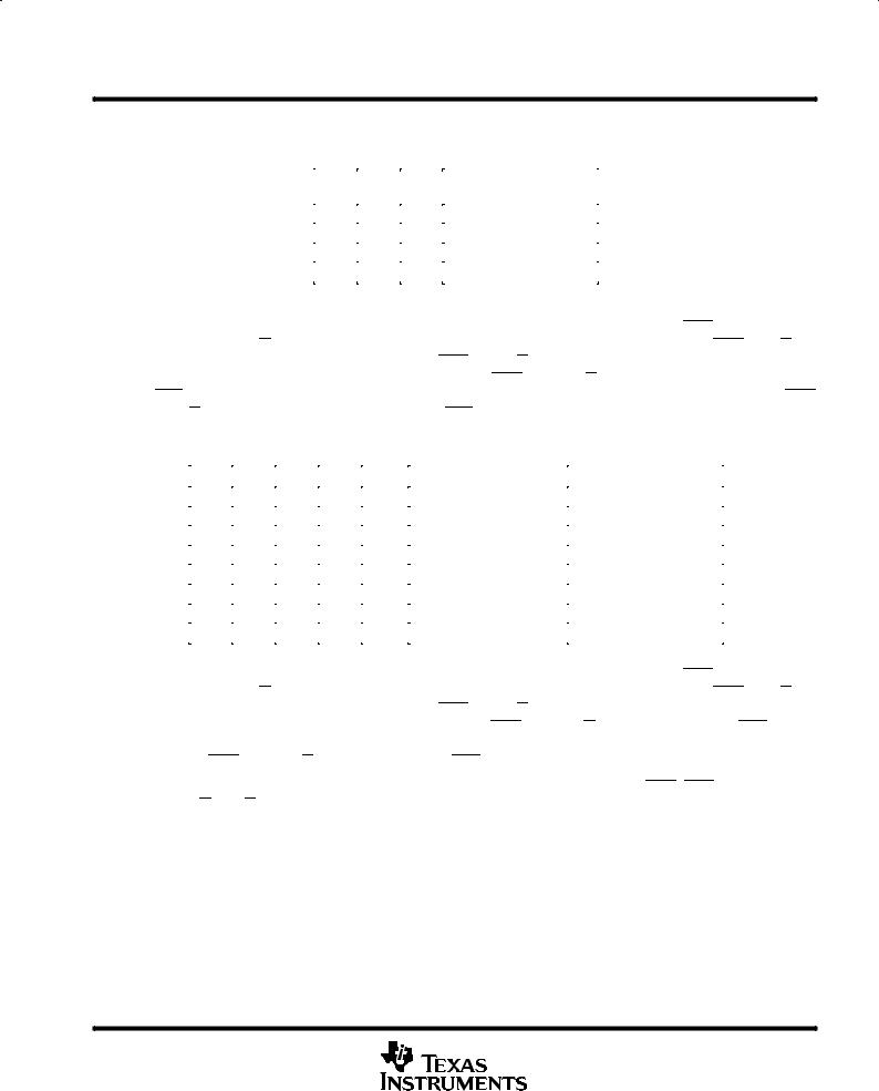
SN74ABT3614 64 ×36 ×2 CLOCKED BIDIRECTIONAL FIRST-IN, FIRST-OUT MEMORY
WITH BUS MATCHING AND BYTE SWAPPING
SCBS126H ± JUNE 1992 ± REVISED APRIL 2000
reset (continued)
Table 1. Flag Programming
|
|
|
|
|
|
|
|
|
|
FS1 |
FS0 |
|
|
|
AF AND AE FLAG |
||||
|
RST |
||||||||
|
OFFSET REGISTER (X) |
||||||||
|
|
|
|
|
|||||
|
|
|
|
|
|
||||
H |
H |
|
↑ |
16 |
|
||||
H |
L |
|
↑ |
12 |
|
||||
L |
H |
|
↑ |
8 |
|
||||
L |
L |
|
↑ |
4 |
|
||||
|
|
|
|
|
|
|
|
|
|
FIFO write/read operation
The state of the port-A data (A0±A35) outputs is controlled by the port-A chip select (CSA) and the port-A write/read select (W/RA). The A0±A35 outputs are in the high-impedance state when either CSA or W/RA is high. The A0±A35 outputs are active when both CSA and W/RA are low. Data is loaded into FIFO1 from the A0±A35 inputs on a low-to-high transition of CLKA when CSA is low, W/RA is high, ENA is high, MBA is low, and FFA is high. Data is read from FIFO2 to the A0±A35 outputs by a low-to-high transition of CLKA when CSA is low, W/RA is low, ENA is high, MBA is low, and EFA is high (see Table 2).
Table 2. Port-A Enable Function Table
|
|
|
|
|
|
|
|
|
|
|
|
|
|
CSA |
W/RA |
ENA |
MBA |
CLKA |
A0 ± A35 OUTPUTS |
PORT FUNCTION |
|||||
|
|
|
|
|
|
|
|
|
|
|
|
|
|
H |
X |
X |
X |
X |
In high-impedance state |
None |
|||||
|
L |
H |
L |
X |
X |
In high-impedance state |
None |
|||||
|
L |
H |
H |
L |
↑ |
In high-impedance state |
FIFO1 write |
|||||
|
L |
H |
H |
H |
↑ |
In high-impedance state |
Mail1 write |
|||||
|
L |
L |
L |
L |
X |
Active, FIFO2 output register |
None |
|||||
|
L |
L |
H |
L |
↑ |
Active, FIFO2 output register |
FIFO2 read |
|||||
|
L |
L |
L |
H |
X |
Active, mail2 register |
None |
|||||
|
|
|
|
|
|
|
|
↑ |
|
|
||
|
L |
L |
H |
H |
Active, mail2 register |
Mail2 read (set |
MBF2 |
high) |
||||
|
|
|
|
|
|
|
|
|
|
|
|
|
The state of the port-B data (B0±B35) outputs is controlled by the port-B chip select (CSB) and the port-B write/read select (W/RB). The B0±B35 outputs are in the high-impedance state when either CSB or W/RB is high. The B0±B35 outputs are active when both CSB and W/RB are low. Data is loaded into FIFO2 from the B0±B35 inputs on a low-to-high transition of CLKB when CSB is low, W/RB is high, ENB is high, FFB is high, and either SIZ0 or SIZ1 is low. Data is read from FIFO1 to the B0±B35 outputs by a low-to-high transition of CLKB when CSB is low, W/RB is low, ENB is high, EFB is high, and either SIZ0 or SIZ1 is low (see Table 3).
The setupand hold-time constraints to the port clocks for the port-chip selects (CSA, CSB) and write/read selects (W/RA, W/RB) are only for enabling write and read operations and are not related to high-impedance control of the data outputs. If a port enable is low during a clock cycle, the port-chip select and write/read select can change states during the setupand hold-time window of the cycle.
POST OFFICE BOX 655303 •DALLAS, TEXAS 75265 |
7 |

SN74ABT3614
64 ×36 ×2 CLOCKED BIDIRECTIONAL FIRST-IN, FIRST-OUT MEMORY
WITH BUS MATCHING AND BYTE SWAPPING
SCBS126H ± JUNE 1992 ± REVISED APRIL 2000
FIFO writer/read operation (continued)
Table 3. Port-B Enable Function Table
|
|
|
|
|
|
|
|
|
|
|
|
|
CSB |
W/RB |
ENB |
SIZ1, SIZ0 |
CLKB |
B0 ± B35 OUTPUTS |
PORT FUNCTION |
||||||
|
|
|
|
|
|
|
|
|
|
|
|
|
|
H |
X |
X |
X |
X |
In high-impedance state |
None |
|||||
|
L |
H |
L |
X |
X |
In high-impedance state |
None |
|||||
|
L |
H |
H |
One, both low |
↑ |
In high-impedance state |
FIFO2 write |
|||||
|
L |
H |
H |
Both high |
↑ |
In high-impedance state |
Mail2 write |
|||||
|
L |
L |
L |
One, both low |
X |
Active, FIFO1 output register |
None |
|||||
|
L |
L |
H |
One, both low |
↑ |
Active, FIFO1 output register |
FIFO1 read |
|||||
|
L |
L |
L |
Both high |
X |
Active, mail1 register |
None |
|||||
|
|
|
|
|
|
|
|
↑ |
|
|
||
|
L |
L |
H |
Both high |
Active, mail1 register |
Mail1 read (set |
MBF1 |
high) |
||||
|
|
|
|
|
|
|
|
|
|
|
|
|
synchronized FIFO flags
Each FIFO flag is synchronized to its port clock through two flip-flop stages. This is done to improve flag reliability by reducing the probability of metastable events on the output when CLKA and CLKB operate asynchronously to one another. EFA, AEA, FFA, and AFA are synchronized to CLKA. EFB, AEB, FFB, and AFB are synchronized to CLKB. Tables 4 and 5 show the relationship of each port flag to FIFO1 and FIFO2.
Table 4. FIFO1 Flag Operation
NUMBER OF 36-BIT |
SYNCHRONIZED |
SYNCHRONIZED |
||||||||
|
TO CLKB |
|
TO CLKA |
|||||||
WORDS IN FIFO1² |
|
|
||||||||
|
|
|
|
|
|
|
|
|
|
|
|
|
|
|
|
|
|
|
|
|
|
|
|
EFB |
AEB |
|
AFA |
|
FFA |
|||
0 |
|
L |
L |
|
H |
|
H |
|||
1 to X |
|
H |
L |
|
H |
|
H |
|||
(X + 1) to [64 ± (X + 1)] |
|
H |
H |
|
H |
|
H |
|||
(64 ± X) to 63 |
|
H |
H |
|
L |
|
H |
|||
64 |
|
H |
H |
|
L |
|
L |
|||
|
|
|
|
|
|
|
|
|
|
|
² X is the value in the AE flag and AF flag offset register.
Table 5. FIFO2 Flag Operation
NUMBER OF 36-BIT |
SYNCHRONIZED |
SYNCHRONIZED |
||||||||
|
TO CLKA |
|
TO CLKB |
|||||||
WORDS IN FIFO2² |
|
|
||||||||
|
|
|
|
|
|
|
|
|
|
|
|
|
|
|
|
|
|
|
|
|
|
|
|
EFA |
AEA |
|
AFB |
FFB |
||||
0 |
|
L |
|
L |
|
H |
H |
|||
1 to X |
|
H |
|
L |
|
H |
H |
|||
(X + 1) to [64 ± (X + 1)] |
|
H |
|
H |
|
H |
H |
|||
(64 ± X) to 63 |
|
H |
|
H |
|
L |
H |
|||
64 |
|
H |
|
H |
|
L |
L |
|||
|
|
|
|
|
|
|
|
|
|
|
² X is the value in the AE flag and AF flag offset register.
8 |
POST OFFICE BOX 655303 •DALLAS, TEXAS 75265 |

SN74ABT3614 64 ×36 ×2 CLOCKED BIDIRECTIONAL FIRST-IN, FIRST-OUT MEMORY
WITH BUS MATCHING AND BYTE SWAPPING
SCBS126H ± JUNE 1992 ± REVISED APRIL 2000
empty flags (EFA, EFB)
The FIFO empty flag is synchronized to the port clock that reads data from its array. When the empty flag is high, new data can be read to the FIFO output register. When the empty flag is low, the FIFO is empty and attempted FIFO reads are ignored. When reading FIFO1 with a byte or word size on port B, EFB is set low when the fourth byte or second word of the last long word is read.
The FIFO read pointer is incremented each time a new word is clocked to the output register. A word written to a FIFO can be read to the FIFO output register in a minimum of three cycles of the empty-flag synchronizing clock; therefore, an empty flag is low if a word in memory is the next data to be sent to the FIFO output register and two cycles of the port clock that reads data from the FIFO have not elapsed since the time the word was written. The FIFO empty flag is set high by the second low-to-high transition of the synchronizing clock and the new data word can be read to the FIFO output register in the following cycle.
A low-to-high transition on an empty-flag synchronizing clock begins the first synchronization cycle of a write if the clock transition occurs at time tsk1, or greater, after the write. Otherwise, the subsequent clock cycle can be the first synchronization cycle (see Figures 13 and 14).
full flags (FFA, FFB)
The FIFO full flag is synchronized to the port clock that writes data to its array. When the full flag is high, a memory location is free in the SRAM to receive new data. No memory locations are free when the full flag is low and attempted writes to the FIFO are ignored.
Each time a word is written to a FIFO, the write pointer is incremented. From the time a word is read from a FIFO, the previous memory location is ready to be written in a minimum of three cycles of the full-flag synchronizing clock. A full flag is low if less than two cycles of the full-flag synchronizing clock have elapsed since the next memory write location has been read. The second low-to-high transition on the full-flag synchronizing clock after the read sets the full flag high and data can be written in the following clock cycle.
A low-to-high transition on a full-flag synchronizing clock begins the first synchronization cycle of a read if the clock transition occurs at time tsk1, or greater, after the read. Otherwise, the subsequent clock cycle can be the first synchronization cycle (see Figures 15 and 16).
almost-empty flags (AEA, AEB)
The FIFO almost-empty flag is synchronized to the port clock that reads data from its array. The almost-empty state is defined by the value of the almost-full and almost-empty offset register (X). This register is loaded with one of four preset values during a device reset (see reset). An AE flag is low when the FIFO contains X or fewer long words in memory and is high when the FIFO contains (X + 1) or more long words.
Two low-to-high transitions of the AE-flag synchronizing clock are required after a FIFO write for the AE flag to reflect the new level of fill; therefore, the AE flag of a FIFO containing (X + 1) or more long words remains low if two cycles of the synchronizing clock have not elapsed since the write that filled the memory to the (X + 1) level. An AE flag is set high by the second low-to-high transition of the synchronizing clock after the FIFO write that fills memory to the (X + 1) level. A low-to-high transition of an AE flag synchronizing clock begins the first synchronization cycle if it occurs at time tsk2, or greater, after the write that fills the FIFO to (X + 1) long words. Otherwise, the subsequent synchronizing clock cycle can be the first synchronization cycle (see Figures 17 and 18).
POST OFFICE BOX 655303 •DALLAS, TEXAS 75265 |
9 |

SN74ABT3614
64 ×36 ×2 CLOCKED BIDIRECTIONAL FIRST-IN, FIRST-OUT MEMORY
WITH BUS MATCHING AND BYTE SWAPPING
SCBS126H ± JUNE 1992 ± REVISED APRIL 2000
almost-full flags (AFA, AFB)
The FIFO almost-full flag is synchronized to the port clock that writes data to its array. The almost-full state is defined by the value of the almost-full and almost-empty offset register (X). This register is loaded with one of four preset values during a device reset (see reset). An almost-full flag is low when the FIFO contains (64 ± X) or more long words in memory and is high when the FIFO contains [64 ± (X + 1)] or fewer long words.
Two low-to-high transitions of the AF-flag synchronizing clock are required after a FIFO read for the AF flag to reflect the new level of fill; therefore, the AF flag of a FIFO containing [64 ± (X + 1)] or fewer words remains low if two cycles of the synchronizing clock have not elapsed since the read that reduced the number of long words in memory to [64 ± (X + 1)]. An AF flag is set high by the second low-to-high transition of the synchronizing clock after the FIFO read that reduces the number of long words in memory to [64 ± (X + 1)]. A low-to-high transition of an AF-flag synchronizing clock begins the first synchronization cycle if it occurs at time tsk2, or greater, after the read that reduces the number of long words in memory to [64 ± (X + 1)]. Otherwise, the subsequent synchronizing clock cycle can be the first synchronization cycle (see Figures 19 and 20).
mailbox registers
Each FIFO has a 36-bit bypass register to pass command and control information between port A and port B without putting it in queue. The mailbox-select (MBA, MBB) inputs choose between a mail register and a FIFO for a port data-transfer operation. A low-to-high transition on CLKA writes A0±A35 data to the mail1 register when a port-A write is selected by CSA, W/RA, and ENA, and MBA is high. A low-to-high transition on CLKB writes B0±B35 data to the mail2 register when a port-B write is selected by CSB, W/RB, and ENB and both SIZ0 and SIZ1 are high. Writing data to a mail register sets the corresponding flag (MBF1 or MBF2) low. Attempted writes to a mail register are ignored while the mail flag is low.
When the port-A data outputs (A0±A35) are active, the data on the bus comes from the FIFO2 output register when MBA is low and from the mail2 register when MBA is high. When the port-B data outputs (B0±B35) are active, the data on the bus comes from the FIFO1 output register when either one or both SIZ1 and SIZ0 are low and from the mail2 register when both SIZ1 and SIZ0 are high. The mail1 register flag (MBF1) is set high by a rising CLKB edge when a port-B read is selected by CSB, W/RB, and ENB and both SIZ1 and SIZ0 are high. The mail2 register flag (MBF2) is set high by a rising CLKA edge when a port-A read is selected by CSA, W/RA, and ENA and MBA is high. The data in the mail register remains intact after it is read and changes only when new data is written to the register.
dynamic bus sizing
The port-B bus can be configured in a 36-bit long word, 18-bit word, or 9-bit byte format for data read from FIFO1 or written to FIFO2. Wordand byte-size bus selections can utilize the most-significant bytes of the bus (big endian) or least-significant bytes of the bus (little endian). Port-B bus size can be changed dynamically and synchronous to CLKB to communicate with peripherals of various bus widths.
The levels applied to the port-B bus-size select (SIZ0, SIZ1) inputs and the big-endian select (BE) input are stored on each CLKB low-to-high transition. The stored port-B bus-size selection is implemented by the next rising edge on CLKB according to Figure 1.
Only 36-bit long-word data is written to or read from the two FIFO memories on the SN74ABT3614. Bus-matching operations are done after data is read from the FIFO1 RAM and before data is written to the FIFO2 RAM. Port-B bus sizing does not apply to mail-register operations.
10 |
POST OFFICE BOX 655303 •DALLAS, TEXAS 75265 |
SN74ABT3614 64 ×36 ×2 CLOCKED BIDIRECTIONAL FIRST-IN, FIRST-OUT MEMORY
WITH BUS MATCHING AND BYTE SWAPPING
|
|
|
|
|
|
|
|
|
|
|
|
|
|
|
|
SCBS126H ± JUNE 1992 ± REVISED APRIL 2000 |
|
|
|
|
|
|
|
|
|
|
|
|
|
|
|
|
|
dynamic bus sizing (continued) |
|
|
|
|
|
|
|
|
|
|
|
|
|
|
|
|
A35 |
A27 |
A26 |
A18 |
A17 |
A9 |
A8 |
|
A0 |
||||||||
|
|
|
|
|
|
|
|
|
|
|
|
|
|
|
Write to FIFO1/Read From FIFO2 |
|
BYTE ORDER ON PORT A: |
|
A |
|
|
|
B |
|
|
|
C |
|
|
|
D |
|
|
|
|
|
|
|
|
|
|
|
|
|
|
|
|
|
|
|
|
|
|
SIZ1 |
SIZ0 |
BE |
||||
|
|
|
|
|
|
X |
L |
L |
|
|
|
|
|
|
|
|
|
|
|
BE |
SIZ1 |
SIZ0 |
||
|
|
|
|
|
|
L |
L |
H |
|
|
|
|
|
|
|
|
|
|
|
BE |
SIZ1 |
SIZ0 |
||
|
|
|
|
|
|
H |
L |
H |
|
|
|
|
|
|
|
|
|
|
|
BE |
SIZ1 |
SIZ0 |
||
|
|
|
|
|
|
L |
H |
L |
|
|
|
|
|
|
B35 |
B27 |
B26 |
B18 |
B17 |
B9 |
B8 |
|
B0 |
||||||||
|
|
|
|
|
|
|
|
|
|
|
|
|
|
|
|
Read From FIFO1/Write to FIFO2 |
|
A |
|
|
|
|
B |
|
|
|
C |
|
|
|
D |
|
|
|
|
|
|
|
|
|
|
|
|
|
|
|
|
|||
|
|
|
|
(a) LONG WORD SIZE |
|
|
|
|
|
|||||||
B35 |
B27 |
B26 |
B18 |
B17 |
B9 |
B8 |
|
B0 |
||||||||
|
|
|
|
|
|
|
|
|
|
|
|
|
|
|
1st: Read From FIFO1/Write to FIFO2 |
|
|
A |
|
|
|
|
B |
|
|
|
|
|
|
|
|
|
|
|
|
|
|
|
|
|
|
|
|
|
|
|
|
|
|
|
B35 |
B27 |
B26 |
B18 |
B17 |
B9 |
B8 |
|
B0 |
||||||||
|
|
|
|
|
|
|
|
|
|
|
|
|
|
|
2nd: Read From FIFO1/Write to FIFO2 |
|
|
C |
|
|
|
|
D |
|
|
|
|
|
|
|
|
|
|
|
|
|
|
|
|
|
|
|
|
|
|
|
||||
|
|
|
|
(b) WORD SIZE ± BIG ENDIAN |
|
|
|
|||||||||
B35 |
B27 |
B26 |
B18 |
B17 |
B9 |
B8 |
|
B0 |
||||||||
|
|
|
|
|
|
|
|
|
|
|
|
|
|
|
1st: Read From FIFO1/Write to FIFO2 |
|
|
|
|
|
|
|
|
|
|
|
C |
|
|
|
D |
|
|
|
|
|
|
|
|
|
|
|
|
|
|
|
|
|
|
|
B35 |
B27 |
B26 |
B18 |
B17 |
B9 |
B8 |
|
B0 |
||||||||
|
|
|
|
|
|
|
|
|
|
|
|
|
|
|
2nd: Read From FIFO1/Write to FIFO2 |
|
|
|
|
|
|
|
|
|
|
|
A |
|
|
|
B |
|
|
|
|
|
|
|
|
|
|
|
|
|
|
|||||
|
|
|
(c) WORD SIZE ± LITTLE ENDIAN |
|
|
|
||||||||||
B35 |
B27 |
B26 |
B18 |
B17 |
B9 |
B8 |
|
B0 |
||||||||
|
|
|
|
|
|
|
|
|
|
|
|
|
|
|
|
1st: Read From FIFO1/Write to FIFO2 |
|
A |
|
|
|
|
|
|
|
|
|
|
|
|
|
|
|
|
|
|
|
|
|
|
|
|
|
|
|
|
|
|
|
|
B35 |
B27 |
B26 |
B18 |
B17 |
B9 |
B8 |
|
B0 |
||||||||
|
B |
|
|
|
|
|
|
|
|
|
|
|
|
|
|
2nd: Read From FIFO1/Write to FIFO2 |
|
|
|
|
|
|
|
|
|
|
|
|
|
|
|
|
|
B35 |
B27 |
B26 |
B18 |
B17 |
B9 |
B8 |
|
B0 |
||||||||
|
|
|
|
|
|
|
|
|
|
|
|
|
|
|
|
3rd: Read From FIFO1/Write to FIFO2 |
|
C |
|
|
|
|
|
|
|
|
|
|
|
|
|
|
|
|
|
|
|
|
|
|
|
|
|
|
|
|
|
|
|
|
B35 |
B27 |
B26 |
B18 |
B17 |
B9 |
B8 |
|
B0 |
||||||||
|
|
|
|
|
|
|
|
|
|
|
|
|
|
|
|
4th: Read From FIFO1/Write to FIFO2 |
|
D |
|
|
|
|
|
|
|
|
|
|
|
|
|
|
|
|
|
|
|
|
|
|
|
|
|
|
|
|
|
|
|
|
(d) BYTE SIZE ± BIG ENDIAN
Figure 1. Dynamic Bus Sizing
POST OFFICE BOX 655303 •DALLAS, TEXAS 75265 |
11 |

SN74ABT3614
64 ×36 ×2 CLOCKED BIDIRECTIONAL FIRST-IN, FIRST-OUT MEMORY
WITH BUS MATCHING AND BYTE SWAPPING
SCBS126H ± JUNE 1992 ± REVISED APRIL 2000
dynamic bus sizing (continued)
|
|
|
|
|
B35 |
B27 |
B26 |
B18 |
B17 |
B9 |
B8 |
B0 |
|||||||||
|
|
|
SIZ1 |
SIZ0 |
|
|
|
|
|
|
|
|
|
|
|
|
|
|
|
|
|
BE |
|
|
|
|
|
|
|
|
|
|
|
|
|
D |
|
1st: Read From FIFO1/Write to FIFO2 |
|||||
|
|
|
|
|
|
|
|
|
|
|
|
|
|
|
|
|
|
|
|||
|
H |
H |
L |
|
|
|
|
|
|
|
|
|
|
|
|
|
|
|
|
||
B35 |
B27 |
B26 |
B18 |
B17 |
B9 |
B8 |
B0 |
||||||||||||||
|
|
|
|
|
|||||||||||||||||
|
|
|
|
|
|||||||||||||||||
|
|
|
|
|
|
|
|
|
|
|
|
|
|
|
|
|
|
|
|
2nd: Read From FIFO1/Write to FIFO2 |
|
|
|
|
|
|
|
|
|
|
|
|
|
|
|
|
|
|
|
C |
|
||
|
|
|
|
|
|
|
|
|
|
|
|
|
|
|
|
|
|
|
|
|
|
|
|
|
|
|
B35 |
B27 |
B26 |
B18 |
B17 |
B9 |
B8 |
B0 |
|||||||||
|
|
|
|
|
|
|
|
|
|
|
|
|
|
|
|
|
|
|
|
3rd: Read From FIFO1/Write to FIFO2 |
|
|
|
|
|
|
|
|
|
|
|
|
|
|
|
|
|
|
|
B |
|
||
|
|
|
|
|
|
|
|
|
|
|
|
|
|
|
|
|
|
|
|
|
|
|
|
|
|
|
B35 |
B27 |
B26 |
B18 |
B17 |
B9 |
B8 |
B0 |
|||||||||
|
|
|
|
|
|
|
|
|
|
|
|
|
|
|
|
|
|
|
|
4th: Read From FIFO1/Write to FIFO2 |
|
|
|
|
|
|
|
|
|
|
|
|
|
|
|
|
|
|
|
A |
|
||
|
|
|
|
|
|
|
|
|
|
|
|
|
|
|
|
|
|
|
|
|
|
(e) BYTE SIZE ± LITTLE ENDIAN
Figure 1. Dynamic Bus Sizing (continued)
bus-matching FIFO1 reads
Data is read from the FIFO1 RAM in 36-bit long-word increments. If a long-word bus size is implemented, the entire long word immediately shifts to the FIFO1 output register. If byte or word size is implemented on port B, only the first one or two bytes appear on the selected portion of the FIFO1 output register with the rest of the long word stored in auxiliary registers. In this case, subsequent FIFO1 reads with the same bus-size implementation output the rest of the long word to the FIFO1 output register in the order shown by Figure 1.
Each FIFO1 read with a new bus-size implementation automatically unloads data from the FIFO1 RAM to its output register and auxiliary registers. Therefore, implementing a new port-B bus size and performing a FIFO1 read before all bytes or words stored in the auxiliary registers have been read results in a loss of the unread long-word data.
When reading data from FIFO1 in byte or word format, the unused B0±B35 outputs remain inactive but static with the unused FIFO1 output register bits holding the last data value to decrease power consumption.
bus-matching FIFO2 writes
Data is written to the FIFO2 RAM in 36-bit long-word increments. FIFO2 writes with a long-word bus size immediately store each long word in FIFO2 RAM. Data written to FIFO2 with a byte or word bus size stores the initial bytes or words in auxiliary registers. The CLKB rising edge that writes the fourth byte or the second word of long word to FIFO2 also stores the entire long word in FIFO2 RAM. The bytes are arranged in the manner shown in Figure 1.
Each FIFO2 write with a new bus-size implementation resets the state machine that controls the data flow from the auxiliary registers to the FIFO2 RAM. Therefore, implementing a new bus size and performing a FIFO2 write before bytes or words stored in the auxiliary registers have been loaded to FIFO2 RAM results in a loss of data.
12 |
POST OFFICE BOX 655303 •DALLAS, TEXAS 75265 |

SN74ABT3614 64 ×36 ×2 CLOCKED BIDIRECTIONAL FIRST-IN, FIRST-OUT MEMORY
WITH BUS MATCHING AND BYTE SWAPPING
SCBS126H ± JUNE 1992 ± REVISED APRIL 2000
port-B mail-register access
In addition to selecting port-B bus sizes for FIFO reads and writes, the port-B bus size select (SIZ0, SIZ1) inputs also access the mail registers. When both SIZ0 and SIZ1 are high, the mail1 register is accessed for a port-B long-word read and the mail2 register is accessed for a port-B long-word write. The mail register is accessed immediately. Any bus-sizing operation that is underway is unaffected by the mail-register access. After the mail-register access is complete, the previous FIFO access can resume in the next CLKB cycle. The logic diagram in Figure 2 shows that the previous bus-size selection is preserved when the mail registers are accessed from port B. A port-B bus size is implemented on each rising CLKB edge according to the states of SIZ0_Q, SIZ1_Q, and BE_Q.
CLKB |
|
|
|
|
MUX |
|
|
|
G1 |
|
|
|
1 |
|
SIZ0_Q |
|
|
|
|
|
D |
Q |
SIZ1_Q |
SIZ0 |
|
|
BE_Q |
|
|
|
|
SIZ1 |
1 |
|
|
BE |
|
|
|
Figure 2. Logic Diagram for SIZ0, SIZ1, and BE Register
byte swapping
The byte-order arrangement of data read from FIFO1 or data written to FIFO2 can be changed synchronous to the rising edge of CLKB. Byte-order swapping is not available for mail-register data. Four modes of byte-order swapping (including no swap) can be done with any data-port-size selection. The order of the bytes is rearranged within the long word, but the bit order within the bytes remains constant.
Byte arrangement is chosen by the port-B swap select (SW0, SW1) inputs on a CLKB rising edge that reads a new long word from FIFO1 or writes a new long word to FIFO2. The byte order chosen on the first byte or first word of a new long-word read from FIFO1 or written to FIFO2 is maintained until the entire long word is transferred, regardless of the SW0 and SW1 states during subsequent writes or reads. Figure 3 is an example of the byte-order swapping available for long words. Performing a byte swap and bus size simultaneously for a FIFO1 read first rearranges the bytes as shown in Figure 3, then outputs the bytes as shown in Figure 1. Simultaneous bus-sizing and byte-swapping operations for FIFO2 writes load the data according to Figure 1, then swap the bytes as shown in Figure 3 when the long word is loaded to FIFO2 RAM.
POST OFFICE BOX 655303 •DALLAS, TEXAS 75265 |
13 |
 Loading...