


Texas Instruments SN65LVDS388DBT, SN65LVDS388DBTR, SN65LVDT386DGG, SN65LVDT386DGGR, SN65LVDT388DBT Datasheet
...SN65LVDS386, SN65LVDT386, SN75LVDS386, SN75LVDT386 SN65LVDS388, SN65LVDT388, SN75LVDS388, SN75LVDT388 HIGH-SPEED DIFFERENTIAL LINE RECEIVERS
SLLS394A ± SEPTEMBER 1999 ± REVISED DECEMBER 1999
DEight (`388) or Sixteen (`386) Line Receivers Meet or Exceed the Requirements of ANSI TIA/EIA-644 Standard
DIntegrated 110-Ω Line Termination
Resistors on LVDT Products
DDesigned for Signaling Rates² Up To 630 Mbps
DSN65 Version's Bus-Terminal ESD Exceeds 15 kV
DOperates From a Single 3.3-V Supply
DTypical Propagation Delay Time of 2.6 ns
DOutput Skew 100 ps (Typ) Part-To-Part Skew is Less Than 1 ns
DLVTTL Levels are 5-V Tolerant
DOpen-Circuit Fail Safe
DFlow-Through Pin Out
DPackaged in Thin Shrink Small-Outline Package With 20-mil Terminal Pitch
description
The `LVDS388 and `LVDT388 (T designates integrated termination) are eight and the `LVDS386 and `LVDT386 sixteen differential line receivers respectively that implement the electrical characteristics of low-voltage differential signaling (LVDS). This signaling technique lowers the output voltage levels of 5-V differential standard levels (such as EIA/TIA-422B) to reduce the power, increase the switching speeds, and allow operation with a 3-V supply rail. Any of the eight or sixteen differential receivers will provide a valid logical output state with a ±100 mV differential input voltage within the input commonmode voltage range. The input common-mode voltage range allows 1 V of ground potential difference between two LVDS nodes. Additionally, the high-speed switching of LVDS signals almost always require the use of a line impedance matching resistor at the receiving end of the cable or transmission media. The LVDT products eliminate this external resistor by integrating it with the receiver.
SN65LVDS388, SN75LVDS388 SN65LVDT388, SN75LVDT388 DBT PACKAGE
(TOP VIEW)
A1A |
|
1 |
38 |
|
GND |
|
|
||||
|
|
||||
A1B |
|
2 |
37 |
|
VCC |
|
|
||||
A2A |
|
3 |
36 |
|
ENA |
|
|
||||
A2B |
|
4 |
35 |
|
A1Y |
|
|
||||
NC |
|
5 |
34 |
|
A2Y |
|
|
||||
B1A |
|
6 |
33 |
|
ENB |
|
7 |
|
|||
B1B |
|
32 |
|
B1Y |
|
|
8 |
|
|||
B2A |
|
31 |
|
B2Y |
|
B2B |
|
9 |
30 |
|
GND |
|
|
||||
|
|
||||
NC |
|
10 |
29 |
|
VCC |
|
11 |
|
|||
C1A |
|
28 |
|
GND |
|
C1B |
|
12 |
27 |
|
C1Y |
|
|
||||
C2A |
|
13 |
26 |
|
C2Y |
|
|
||||
C2B |
|
14 |
25 |
|
ENC |
|
|
||||
NC |
|
15 |
24 |
|
D1Y |
|
|
||||
D1A |
|
16 |
23 |
|
D2Y |
|
|
||||
D1B |
|
17 |
22 |
|
END |
|
|
||||
D2A |
|
18 |
21 |
|
VCC |
|
|
||||
|
|
|
|||
D2B |
|
19 |
20 |
|
GND |
|
|
|
|
|
|
|
|
|
|
|
|
SN65LVDS386, SN75LVDS386 SN65LVDT386, SN75LVDT386 DGG PACKAGE
(TOP VIEW)
A1A |
|
|
1 |
64 |
|
GND |
|
|
|
||||
A1B |
|
|
2 |
63 |
|
VCC |
A2A |
|
|
3 |
62 |
|
VCC |
A2B |
|
|
4 |
61 |
|
GND |
A3A |
|
|
5 |
60 |
|
ENA |
A3B |
|
|
6 |
59 |
|
A1Y |
A4A |
|
|
7 |
58 |
|
A2Y |
A4B |
|
|
8 |
57 |
|
A3Y |
B1A |
|
|
9 |
56 |
|
A4Y |
B1B |
|
|
10 |
55 |
|
ENB |
B2A |
|
|
11 |
54 |
|
B1Y |
B2B |
|
|
12 |
53 |
|
B2Y |
B3A |
|
|
13 |
52 |
|
B3Y |
B3B |
|
|
14 |
51 |
|
B4Y |
B4A |
|
|
15 |
50 |
|
GND |
B4B |
|
|
16 |
49 |
|
VCC |
C1A |
|
|
17 |
48 |
|
VCC |
C1B |
|
|
18 |
47 |
|
GND |
C2A |
|
|
19 |
46 |
|
C1Y |
C2B |
|
|
20 |
45 |
|
C2Y |
C3A |
|
|
21 |
44 |
|
C3Y |
C3B |
|
|
22 |
43 |
|
C4Y |
C4A |
|
|
23 |
42 |
|
ENC |
C4B |
|
24 |
41 |
|
D1Y |
|
D1A |
|
25 |
40 |
|
D2Y |
|
D1B |
|
26 |
39 |
|
D3Y |
|
D2A |
|
27 |
38 |
|
D4Y |
|
D2B |
|
28 |
37 |
|
END |
|
D3A |
|
|
29 |
36 |
|
GND |
D3B |
|
30 |
35 |
|
VCC |
|
D4A |
|
31 |
34 |
|
VCC |
|
D4B |
|
32 |
33 |
|
GND |
|
|
|
|
|
|
|
|
Please be aware that an important notice concerning availability, standard warranty, and use in critical applications of Texas Instruments semiconductor products and disclaimers thereto appears at the end of this data sheet.
² Signaling rate, 1/t, where t is the minimum unit interval and is expressed in the units bits/s (bits per second)
PRODUCTION DATA information is current as of publication date. Products conform to specifications per the terms of Texas Instruments standard warranty. Production processing does not necessarily include testing of all parameters.
Copyright 1999, Texas Instruments Incorporated
POST OFFICE BOX 655303 •DALLAS, TEXAS 75265 |
1 |
SN65LVDS386, SN65LVDT386, SN75LVDS386, SN75LVDT386
SN65LVDS388, SN65LVDT388, SN75LVDS388, SN75LVDT388
HIGH-SPEED DIFFERENTIAL LINE RECEIVERS
SLLS394A ± SEPTEMBER 1999 ± REVISED DECEMBER 1999
description (continued)
The intended application of this device and signaling technique is for point-to-point baseband data transmission over controlled impedance media of approximately 100 Ω. The transmission media may be printed circuit board traces, backplanes, or cables. The large number of receivers integrated into the same substrate along with the low pulse skew of balanced signaling, allows extremely precise timing alignment of clock and data for synchronous parallel data transfers. When used with its companion, 8- or 16-channel driver, the SN65LVDS389 or SN65LVDS387, over 300 million data transfers per second in single-edge clocked systems are possible with very little power. (Note: The ultimate rate and distance of data transfer is dependent upon the attenuation characteristics of the media, the noise coupling to the environment, and other system characteristics.)
Available Options
Part number |
Temperature |
Number of |
Bus-Pin ESD |
|
Range |
Receivers |
|||
|
|
|||
|
|
|
|
|
SN65LVDS386DGG |
±40_C to 85_C |
16 |
15 kV |
|
|
|
|
|
|
SN65LVDT386DGG |
±40_C to 85_C |
16 |
15 kV |
|
|
|
|
|
|
SN75LVDS386DGG |
0_C to 70_C |
16 |
4 kV |
|
|
|
|
|
|
SN75LVDT386DGG |
0_C to 70_C |
16 |
4 kV |
|
|
|
|
|
|
SN65LVDS388DBT |
±40_C to 85_C |
8 |
15 kV |
|
|
|
|
|
|
SN65LVDT388DBT |
±40_C to 85_C |
8 |
15 kV |
|
|
|
|
|
|
SN75LVDS388DBT |
0_C to 70_C |
8 |
4 kV |
|
|
|
|
|
|
SN75LVDT388DBT |
0_C to 70_C |
8 |
4 kV |
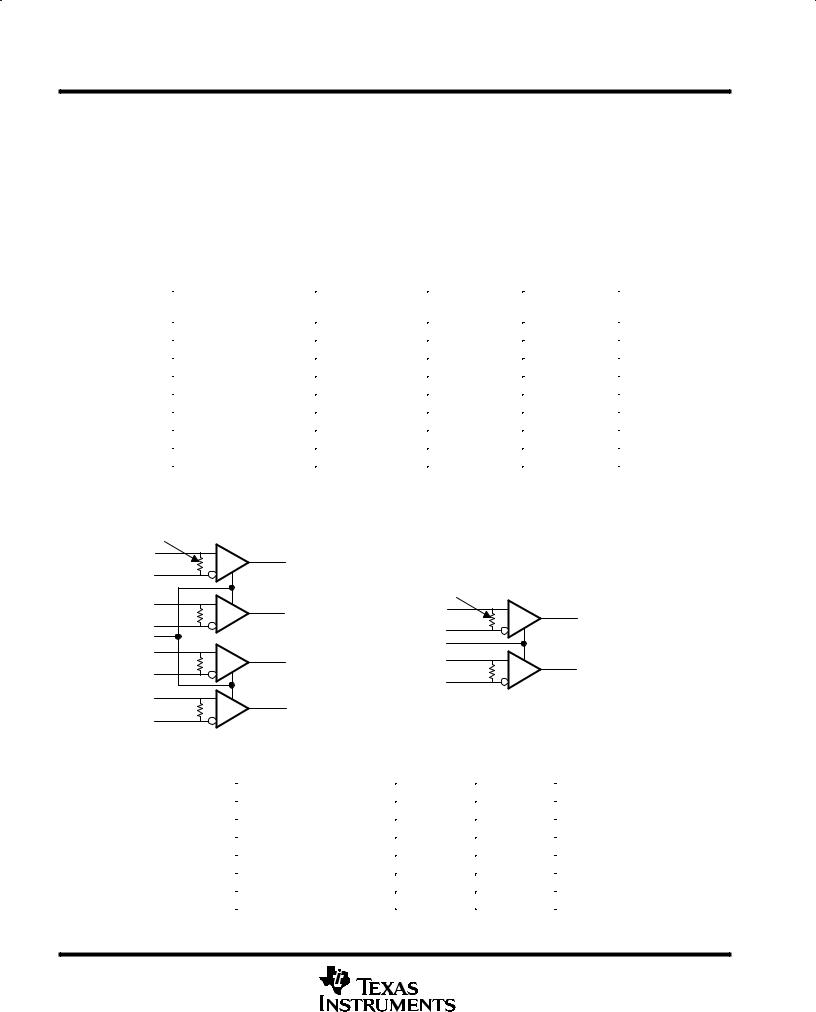
logic diagram (positive logic)
'LVDx386 |
|
|
'LVDT386 ONLY |
|
|
1A |
'LVDx388 |
|
1Y |
|
|
1B |
|
|
|
'LVDT388 ONLY |
|
2A |
1A |
|
2Y |
||
1Y |
||
2B |
||
1B |
||
EN |
||
EN |
||
3A |
||
2A |
||
3Y |
||
3B |
2Y |
|
2B |
||
|
||
4A |
|
|
4Y |
|
|
4B |
|
Function Table
SNx5LVD386/388 and SNx5LVDT386/388
DIFFERENTIAL INPUT |
|
ENABLES |
OUTPUT |
|
|
|
|
|
|
|
A-B |
|
EN |
Y |
|
|
|
|
|
VID ≥ |
100 mV |
|
H |
H |
-100 mV < VID ≤ 100 mV |
|
H |
? |
|
VID ≤ -100 mV |
|
H |
L |
|
|
X |
|
L |
Z |
|
|
|
|
|
Open |
|
H |
H |
|
H = high level, |
L = low level, |
X = irrelevant, |
|
|
Z = high impedance (off), ? = indeterminate
2 |
POST OFFICE BOX 655303 •DALLAS, TEXAS 75265 |

SN65LVDS386, SN65LVDT386, SN75LVDS386, SN75LVDT386
SN65LVDS388, SN65LVDT388, SN75LVDS388, SN75LVDT388
HIGH-SPEED DIFFERENTIAL LINE RECEIVERS
SLLS394A ± SEPTEMBER 1999 ± REVISED DECEMBER 1999
equivalent input and output schematic diagrams
VCC |
VCC |
VCC |
300 kΩ |
300 kΩ |
|
|
100 Ω |
5 Ω |
|
EN |
Y Output |
|
|
|
A Input |
B Input 7 V |
7 V |
|
300 kΩ |
|
7 V |
7 V |
|
110 Ω
'LVDT Devices Only
absolute maximum ratings over operating free-air temperature (unless otherwise noted)²
Supply voltage range, VCC (see Note 1) . . . . . . . . . . . . . . . . . . . . . . . . . . . . . . . . . |
. . . . . . . . . . . . . ±0.5 V to 4 V |
|
Voltage range: |
Enables or Y . . . . . . . . . . . . . . . . . . . . . . . . . . . . . . . . . . . . . . |
. . . . . . . ±0.5 V to VCC + 2 V |
|
A or B . . . . . . . . . . . . . . . . . . . . . . . . . . . . . . . . . . . . . . . . . . . . |
. . . . . . . . . . . . . ±0.5 V to 4 V |
Electrostatic discharge: (see Note 2) |
|
|
|
SN65' (A, B, and GND) . . . . . . . . . . . . . . . . . . . . . . . . . . |
. . Class 3, A:15 kV, B: 700 V |
|
SN65' (All pins) . . . . . . . . . . . . . . . . . . . . . . . . . . . . . . . . . |
. . . Class 3, A: 8 kV, B:600 V |
|
SN75' (A, B, and GND) . . . . . . . . . . . . . . . . . . . . . . . . . . |
. . . Class 2, A:4 kV, B: 400 V |
|
SN75' (All pins) . . . . . . . . . . . . . . . . . . . . . . . . . . . . . . . . . |
. . . Class 2, A: 2 kV, B:200 V |
Continuous power dissipation . . . . . . . . . . . . . . . . . . . . . . . . . . . . . . . . . . . . . . . . . |
See Dissipation Rating Table |
|
Storage temperature range . . . . . . . . . . . . . . . . . . . . . . . . . . . . . . . . . . . . . . . . . . . . . |
. . . . . . . . . . . ±65°C to 150°C |
|
Lead temperature 1,6 mm (1/16 in) from case for 10 seconds . . . . . . . . . . . . . . . |
. . . . . . . . . . . . . . . . . . . 260°C |
|
²Stresses beyond those listed under ªabsolute maximum ratingsº may cause permanent damage to the device. These are stress ratings only, and functional operation of the device at these or any other conditions beyond those indicated under ªrecommended operating conditionsº is not implied. Exposure to absolute-maximum-rated conditions for extended periods may affect device reliability.
NOTES: 1. All voltage values, except differential I/O bus voltages, are with respect to network ground terminal. 2. Tested in accordance with MIL-STD-883C Method 3015.7.
DISSIPATION RATING TABLE
|
|
DERATING FACTOR³ |
T = 70°C |
T = 85°C |
PACKAGE |
TA ≤ 25°C |
ABOVE TA = 25°C |
A |
A |
POWER RATING |
POWER RATING |
|||
DBT |
1071 mW |
8.5 mW/°C |
688 mW |
556 mW |
|
|
|
|
|
DGG |
2094 mW |
16.7 mW/°C |
1342 mW |
1089 mW |
³ This is the inverse of the junction-to-ambient thermal resistance when board-mounted (low-k) and with no air flow.
POST OFFICE BOX 655303 •DALLAS, TEXAS 75265 |
3 |
SN65LVDS386, SN65LVDT386, SN75LVDS386, SN75LVDT386
SN65LVDS388, SN65LVDT388, SN75LVDS388, SN75LVDT388
HIGH-SPEED DIFFERENTIAL LINE RECEIVERS
SLLS394A ± SEPTEMBER 1999 ± REVISED DECEMBER 1999
recommended operating conditions
|
|
|
MIN |
NOM |
|
MAX |
UNIT |
|||
|
|
|
|
|
|
|
|
|
|
|
Supply voltage, VCC |
3 |
3.3 |
|
3.6 |
V |
|||||
High-level input voltage, VIH |
2 |
|
|
|
|
|
V |
|||
Low-level input voltage, VIL |
|
|
|
|
|
0.8 |
V |
|||
Magnitude of differential input voltage, VID |
0.1 |
|
|
0.6 |
V |
|||||
|
|
|
|VID| |
|
|
2.4 |
|
|VID| |
|
|
Common±mode input voltage, VIC (see Figure 4) |
2 |
|
V |
|||||||
|
|
2 |
|
|||||||
|
|
|
|
|||||||
|
|
|
|
|
|
VCC ± 0.8 |
|
|||
Operating free-air temperature, TA |
SN75' |
0 |
|
|
70 |
°C |
||||
|
|
|
|
|
|
|
|
|
|
|
SN65' |
± 40 |
|
|
85 |
°C |
|||||
|
|
|
||||||||
|
|
|
|
|
|
|
|
|
|
|
4 |
POST OFFICE BOX 655303 •DALLAS, TEXAS 75265 |
SN65LVDS386, SN65LVDT386, SN75LVDS386, SN75LVDT386
SN65LVDS388, SN65LVDT388, SN75LVDS388, SN75LVDT388
HIGH-SPEED DIFFERENTIAL LINE RECEIVERS
SLLS394A ± SEPTEMBER 1999 ± REVISED DECEMBER 1999
electrical characteristics over recommended operating conditions (unless otherwise noted).
|
PARAMETER |
|
TEST CONDITIONS |
MIN |
TYP² |
MAX |
UNIT |
||
VITH+ |
Positive±going differential input voltage threshold |
|
See Figure 1 and Table 1 |
|
|
100 |
mV |
||
VITH± |
Negative±going differential input voltage threshold |
±100 |
|
|
mV |
||||
|
|
|
|
||||||
VOH |
High±level output voltage |
|
IOH = ±8 mA |
|
2.4 |
3 |
|
V |
|
VOL |
Low±level output voltage |
|
IOL = 8 mA |
|
|
0.2 |
0.4 |
V |
|
ICC |
Supply current |
|
Enabled, |
No load |
|
50 |
70 |
mA |
|
|
|
|
|
|
|
||||
|
Disabled |
|
|
|
3 |
||||
|
|
|
|
|
|
|
|
||
|
|
|
|
|
|
|
|
|
|
|
|
|
'LVDS |
VI = 0 V |
|
|
±13 |
±20 |
|
II |
Input current (A or B inputs) |
|
VI = 2.4 V |
|
±1.2 |
±3 |
|
µA |
|
|
|
|
|
||||||
|
'LVDT |
VI = 0 V, other input open |
|
|
±40 |
||||
|
|
|
|
|
|
||||
|
|
|
VI = 2.4 V, other input open |
±2.4 |
|
|
|
||
|
|
|
|
|
|
|
|||
IID |
Differential input current |IIA ± IIB| |
|
`LVDS |
VIA= 0 V, |
VIB = 0.1V, |
|
|
±2 |
µA |
|
VIA= 2.4 V, |
VIB = 2.3 V |
|
|
|||||
|
|
|
|
|
|
|
|
||
IID |
Differential input current (IIA ± IIB) |
|
`LVDT |
VIA= 0.2 V, |
VIB = 0V, |
1.5 |
|
2.2 |
mA |
|
VIA= 2.4 V, |
VIB = 2.2 V |
|
||||||
|
|
|
|
|
|
|
|
||
II(OFF) |
Power±off Input current (A or B inputs) |
|
`LVDS |
VCC = 0 V, |
VI=2.4 V |
|
12 |
±20 |
µA |
II(OFF) |
Power±off Input current (A or B inputs) |
|
`LVDT |
VCC = 0 V, |
VI=2.4 V |
|
|
±40 |
µA |
IIH |
High±level input current (enables) |
|
VIH = 2 V |
|
|
|
10 |
µA |
|
IIL |
Low±level input current (enables) |
|
VIL = 0.8 V |
|
|
|
10 |
µA |
|
IOZ |
High±impedance output current |
|
VO = 0 V |
|
|
|
±1 |
µA |
|
|
VO = 3.6 V |
|
|
|
10 |
||||
|
|
|
|
|
|
|
|
||
CIN |
Input Capacitance, A or B input to GND |
|
VID = 0.4 sin 2.5E09 t V |
|
5 |
|
pF |
||
Z(t) |
Termination impedance |
|
VID = 0.4 sin 2.5E09 t V |
88 |
|
132 |
Ω |
||
² All typical values are at 25°C and with a 3.3 V supply. |
|
|
|
|
|
|
|
||
switching characteristics over recommended operating conditions (unless otherwise noted)
|
PARAMETER |
TEST CONDITIONS |
MIN |
TYP² |
MAX |
UNIT |
tPLH |
Propagation delay time, low-to-high-level output |
|
1 |
2.6 |
4 |
ns |
tPHL |
Propagation delay time, high-to-low-level output |
|
1 |
2.5 |
4 |
ns |
tr |
Differential output signal rise time |
|
500 |
800 |
1200 |
ps |
tf |
Differential output signal fall time |
See Figure 2 |
500 |
800 |
1200 |
ps |
tsk(p) |
Pulse skew (|tPHL ± tPLH|) |
|
|
150 |
600 |
ps |
t |
Output skew³ |
|
|
100 |
400 |
ps |
sk(o) |
|
|
|
|
|
|
t |
Part-to-part skew§ |
|
|
|
1 |
ns |
sk(pp) |
|
|
|
|
|
|
tPZH |
Propagation delay time, high-impedance-to-high-level output |
|
|
7 |
15 |
ns |
tPZL |
Propagation delay time, high-impedance-to-low-level output |
See Figure 3 |
|
7 |
15 |
ns |
tPHZ |
Propagation delay time, high-level-to-high-impedance output |
|
7 |
15 |
ns |
|
|
|
|||||
tPLZ |
Propagation delay time, low-level-to-high-impedance output |
|
|
7 |
15 |
ns |
² All typical values are at 25°C and with a 3.3 V supply.
³ tsk(o) is the magnitude of the time difference between the tPLH or tPHL of all drivers of a single device with all of their inputs connected together.
§tsk(pp) is the magnitude of the difference in propagation delay times between any specified terminals of two devices when both devices operate with the same supply voltages, at the same temperature, and have identical packages and test circuits.
POST OFFICE BOX 655303 •DALLAS, TEXAS 75265 |
5 |
 Loading...