


SN74ACT3638-15PQ
Texas Instruments SN74ACT3638-15PQ, SN74ACT3638-20PCB, SN74ACT3638-20PQ, SN74ACT3638-30PCB, SN74ACT3638-30PQ Datasheet
...
SN74ACT3638
512 × 32 × 2
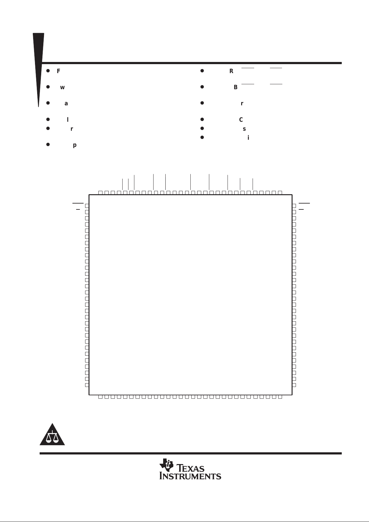
CLOCKED BIDIRECTIONAL FIRST-IN, FIRST-OUT MEMORY
SCAS228D – JUNE 1992 – REVISED APRIL 1998
1
POST OFFICE BOX 655303 • DALLAS, TEXAS 75265
D
Free-Running CLKA and CLKB Can Be
Asynchronous or Coincident
D
Two Independent 512 × 32 Clocked FIFOs
Buffering Data in Opposite Directions
D
Read Retransmit Capability From FIFO on
Port B
D
Mailbox-Bypass Register for Each FIFO
D
Programmable Almost-Full and
Almost-Empty Flags
D
Microprocessor Interface Control Logic
D
IRA, ORA, AEA, and AFA Flags
Synchronized by CLKA
D
IRB, ORB, AEB, and AFB Flags
Synchronized by CLKB
D
Low-Power 0.8-µm Advanced CMOS
T echnology
D
Supports Clock Frequencies up to 67 MHz
D
Fast Access Times of 11 ns
D
Package Options Include 120-Pin Thin
Quad Flat (PCB) and 132-Pin Quad Flat
(PQ) Packages
49
48
47
46
45
44
43
42
41
40
39
38
37
36
35
34
33
32
31
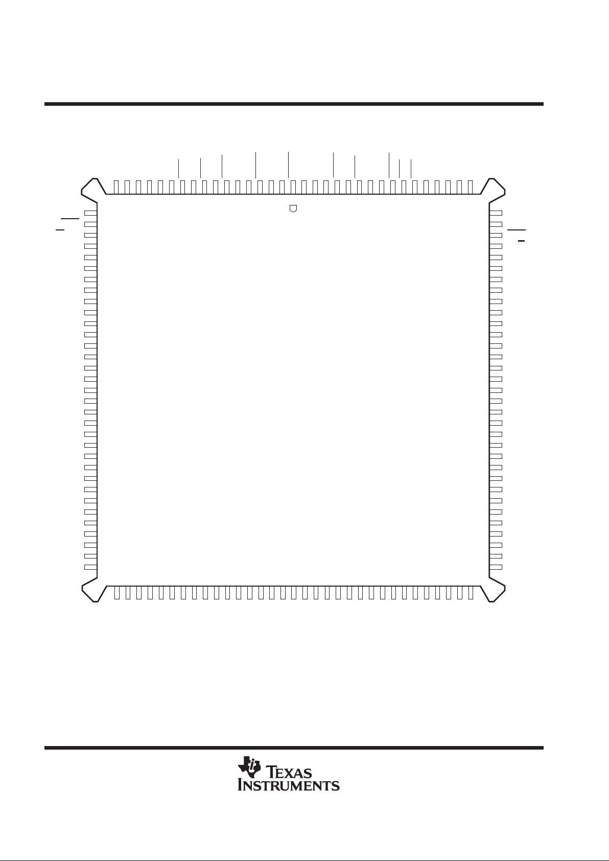
PCB PACKAGE
(TOP VIEW)
CSA
W/RA
ENA
CLKA
V
CC
A31
A30
GND
A29
A28
A27
A26
A25
A24
A23
GND
A22
V
CC
A21
A20
A19
A18
GND
A17
A16
A15
A14
A13
V
CC
A12
CSB
W/RB
ENB
CLKB
GND
B31
B30
B29
B28
B27
B26
V
CC
B25
B24
GND
B23
B22
B21
B20
B19
B18
GND
B17
B16
V
CC
B15
B14
B13
B12
GND
GND
IRA
ORA
A9
A8
GND
A1 1
A10
AFA
AEA
MBF2
RDYA
MBA
RFM
GND
RDYB
FS0
FS1
RSTB
MBB
GND
AEB
NC
A4
A7
A6
A5
A1
A0
B2
GND
B0
B1
B5
GND
B6
50
1
2
3
4
5
6
7
8
9
10
11
12
13
14
15
16
17
18
19
20
21
22
23
24
25
26
27
28
29
30
90
89
88
87
86
85
84
83
82
81
80
79
78
77
76
75
74
73
72
71
70
69
68
67
66
65
64
63
62
61
AFB
NC
ORB
IRB
54
53
52
51
B8
B9
B7
B10
55
56
57
58
59
60
V
CC
RTM
V
CC
A2
96
97
98
99
100
101
102
103
104
105
106
107
108
109
110
111
112
113
114
115
116
117
118
119
120
91
92
93
94
95
RSTA
MBF1
B4
V
CC
NC – No internal connection
V
CC
V
CC
GND
GND
A3
B3
V
CC
B1 1
Copyright 1998, Texas Instruments Incorporated
PRODUCTION DATA information is current as of publication date.
Products conform to specifications per the terms of Texas Instruments
standard warranty. Production processing does not necessarily include
testing of all parameters.
Please be aware that an important notice concerning availability, standard warranty, and use in critical applications of
Texas Instruments semiconductor products and disclaimers thereto appears at the end of this data sheet.
SN74ACT3638
512 × 32 × 2
CLOCKED BIDIRECTIONAL FIRST-IN, FIRST-OUT MEMORY
SCAS228D – JUNE 1992 – REVISED APRIL 1998
2
POST OFFICE BOX 655303 • DALLAS, TEXAS 75265
132
131
130
129
128
127
126
125
124
123
122
121
120
119
118
117
116
115
114
113
112
111
110
109
108
107
106
105
104
103
102
101
100
99
98
97
96
95
94
93
92
91
90
89
88
87
86
85
84
5251 83828180797877767574737271706968676665646362616059585756555453
50
49
48
47
46
45
44
43
42
41
40
39
38
37
36
35
34
33
32
31
30
29
28
27
26
25
24
23
22
21
20
19
18
17 16 15 14 13 12 11 10 9 8 7 6 5 4 3 2
1
NC
CSB
W/RB
ENB
CLKB
GND
B31
B30
B29
B28
B27
B26
V
CC
B25
B24
GND
B23
B22
B21
B20
B19
B18
GND
B17
B16
V
CC
B15
B14
B13
B12
GND
NC
NC
NC
NC
CSA
W/RA
ENA
CLKA
V
CC
A31
A30
GND
A29
A28
A27
A26
A25
A24
A23
GND
A22
V
CC
A21
A20
A19
A18
GND
A17
A16
A15
A14
A13
V
CC
A12
NC
PQ PACKAGE
†
(TOP VIEW)
NC
NC
V
IRB
ORB
NC
GND
AEB
GND
MBF1
MBB
FS1
FS0
RDYB
GND
RFM
RTM
RDYA
RST1
MBA
MBF2
AEA
AFA
NC
ORA
IRA
GND
NC
NC
B1 1
B10
B9
B8
B7
CC
B6
GND
B5
B4
B3
B2
B1
B0
GND
A0
A1
A2
A3
A4
A5
GND
A6
A7
A8
A9
A10
A1 1
GND
NC
NC
CC
V
CC
V
CC
V
CC
V
RST2
AFB
V
CC
NC – No internal connection
†
Uses Yamaichi socket IC51-1324-828

SN74ACT3638
512 × 32 × 2
CLOCKED BIDIRECTIONAL FIRST-IN, FIRST-OUT MEMORY
SCAS228D – JUNE 1992 – REVISED APRIL 1998
3
POST OFFICE BOX 655303 • DALLAS, TEXAS 75265
description
The SN74ACT3638 is a high-speed, low-power CMOS clocked bidirectional FIFO memory. It supports clock
frequencies up to 67 MHz and has read access times as fast as 11 ns. Two independent 512 × 32 dual-port
SRAM FIFOs on the chip buffer data in opposite directions. The FIFO memory buffering data from port A to port
B has retransmit capability, which allows previously read data to be accessed again. Each FIFO has flags to
indicate empty and full conditions and two programmable flags (almost full and almost empty) to indicate when
a selected number of words is stored in memory . Communication between each port can bypass the FIFOs via
two 32-bit mailbox registers. Each mailbox register has a flag to signal when new mail has been stored. Two
or more devices can be used in parallel to create wider datapaths.
The SN74ACT3638 is a clocked FIFO, which means each port employs a synchronous interface. All data
transfers through a port are gated to the low-to-high transition of a continuous (free-running) port clock by enable
signals. The continuous clocks for each port are independent of one another and can be asynchronous or
coincident. The enables for each port are arranged to provide a simple bidirectional interface between
microprocessors and/or buses with synchronous control.
The input-ready (IRA, IRB) flags and almost-full (AFA
, AFB) flags of the SN74ACT3638 are two-stage
synchronized to the port clock that writes data to its array . The output-ready (ORA, ORB) flags and almost-empty
(AEA
, AEB) flags of the SN74ACT3638 are two-stage synchronized to the port clock that reads data from its
array. Offsets for the almost-full and almost-empty flags of both FIFOs can be programmed from port A.
The SN74ACT3638 is characterized for operation from 0°C to 70°C.
For more information on this device family , see the application reports
FIFO Mailbox-Bypass Registers: Using
Bypass Registers to Initialize DMA Control
(literature number SCAA007) and
Metastability Performance of
Clocked FIFOs
(literature number SCZA004).
SN74ACT3638
512 × 32 × 2
CLOCKED BIDIRECTIONAL FIRST-IN, FIRST-OUT MEMORY
SCAS228D – JUNE 1992 – REVISED APRIL 1998
4
POST OFFICE BOX 655303 • DALLAS, TEXAS 75265
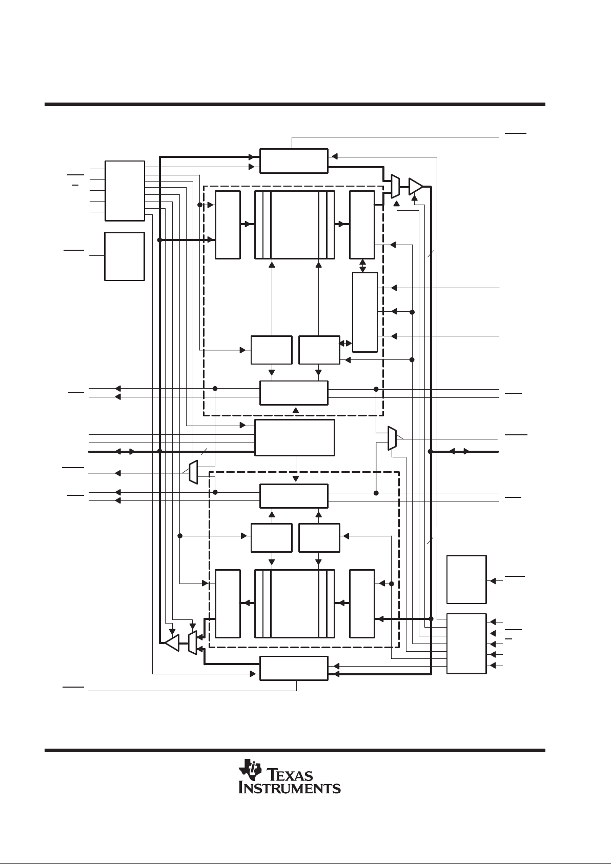
functional block diagram
Port-A
Control
Logic
CLKA
CSA
W/RA
ENA
MBA
FIFO1,
Mail1
Reset
Logic
RST1
512 × 32
SRAM
Input Register
Output Register
Mail1
Register
Write
Pointer
Read
Pointer
Status-Flag
Logic
Programmable-
Flag
Offset Registers
Status-Flag
Logic
Read
Pointer
Write
Pointer
512 × 32
SRAM
Input Register
Output Register
Mail2
Register
Port-B
Control
Logic
IRA
AFA
FS0
FS1
A0–A31
ORA
AEA
MBF2
FIFO2,
Mail2
Reset
Logic
MBF1
ORB
AEB
B0–B31
IRB
AFB
RST2
CLKB
CSB
W/RB
ENB
MBB
FIFO1
FIFO2
9
Sync Retransmit
Logic
RTM
RFM
RDYB
RDY A
32
32
SN74ACT3638
512 × 32 × 2
CLOCKED BIDIRECTIONAL FIRST-IN, FIRST-OUT MEMORY
SCAS228D – JUNE 1992 – REVISED APRIL 1998
5
POST OFFICE BOX 655303 • DALLAS, TEXAS 75265
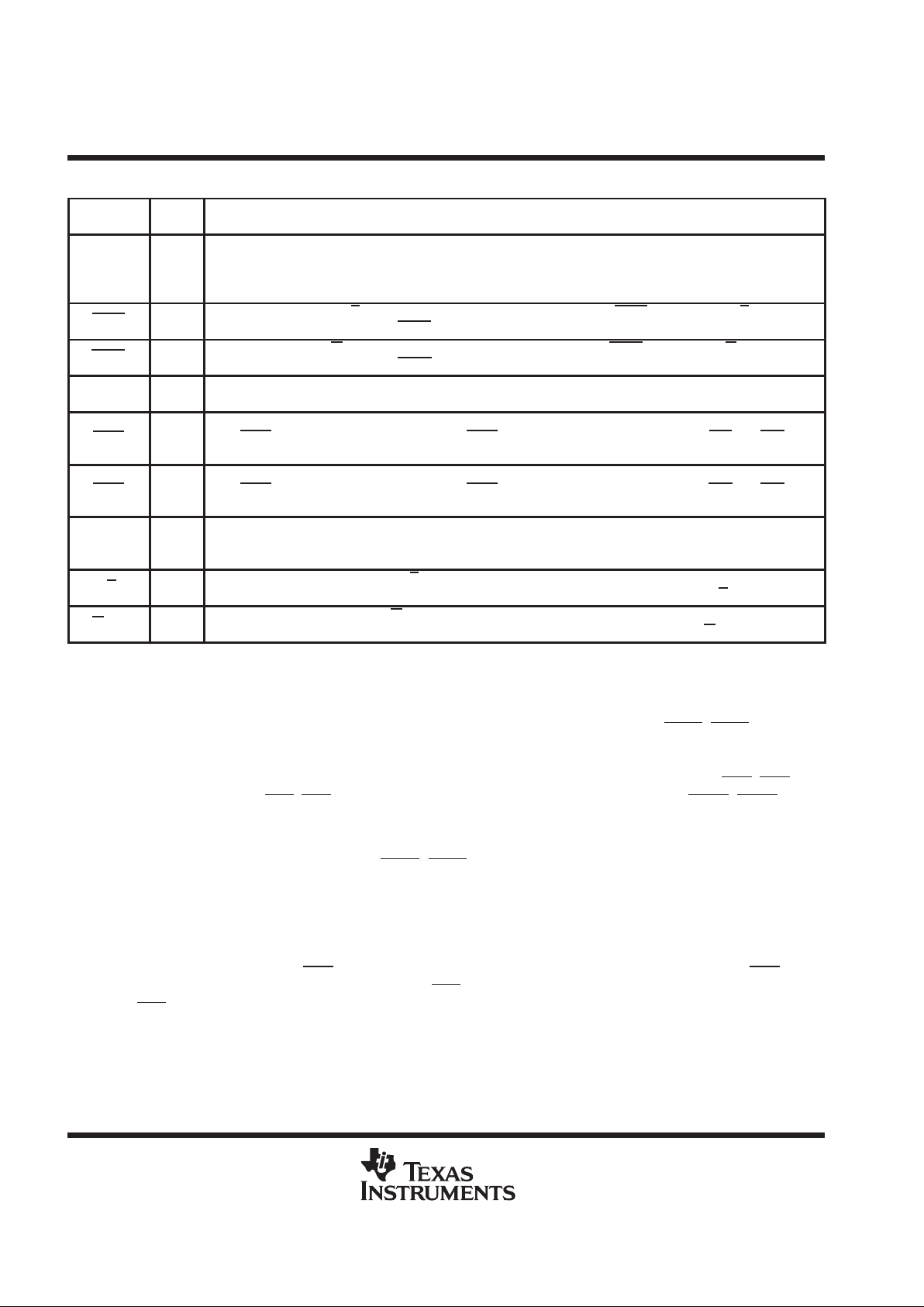
Terminal Functions
TERMINAL
NAME
I/O DESCRIPTION
A0–A31 I/O Port-A data. The 32-bit bidirectional data port for side A.
AEA
O
(port A)
Port-A almost-empty flag. Programmable flag synchronized to CLKA. AEA is low when the number of words in FIFO2
is less than or equal to the value in the almost-empty A offset register, X2.
AEB
O
(port B)
Port-B almost-empty flag. Programmable flag synchronized to CLKB. AEB is low when the number of words in FIFO1
is less than or equal to the value in the almost-empty B offset register, X1.
AFA
O
(port A)
Port-A almost-full flag. Programmable flag synchronized to CLKA. AFA is low when the number of empty locations in
FIFO1 is less than or equal to the value in the almost-full A offset register , Y1.
AFB
O
(port B)
Port-B almost-full flag. Programmable flag synchronized to CLKB. AFB is low when the number of empty locations
in FIFO2 is less than or equal to the value in the almost full B offset register , Y2.
B0–B31 I/O Port-B data. The 32-bit bidirectional data port for side B.
CLKA I
Port-A clock. CLKA is a continuous clock that synchronizes all data transfers through port A and can be asynchronous
or coincident to CLKB. IRA, ORA, AFA
, and AEA are synchronous to the low-to-high transition of CLKA.
CLKB I
Port-B clock. CLKB is a continuous clock that synchronizes all data transfers through port B and can be asynchronous
or coincident to CLKA. IRB, ORB, AFB
, and AEB are synchronous to the low-to-high transition of CLKB.
CSA I
Port-A chip select. CSA must be low to enable a low-to-high transition of CLKA to read or write data on port A. The
A0–A31 outputs are in the high-impedance state when CSA
is high.
CSB I
Port-B chip select. CSB must be low to enable a low-to-high transition of CLKB to read or write data on port B. The
B0 –B31 outputs are in the high-impedance state when CSB
is high.
ENA I Port-A enable. ENA must be high to enable a low-to-high transition of CLKA to read or write data on port A.
ENB I Port-B enable. ENB must be high to enable a low-to-high transition of CLKB to read or write data on port B.
FS1, FS0 I
Flag-offset selects. The low-to-high transition of a FIFO reset input latches the values of FS0 and FS1. If either FS0
or FS1 is high when a reset input goes high, one of three preset values is selected as the offset for the FIFO almost-full
and almost-empty flags. If both FIFOs are reset simultaneously and both FS0 and FS1 are low when RST1
and RST2
go high, the first four writes to FIFO1 program the almost-full and almost-empty offsets for both FIFOs.
IRA
O
(port A)
Port-A input-ready flag. IRA is synchronized to the low-to-high transition of CLKA. When IRA is low, FIFO1 is full and
writes to its array are disabled. When FIFO1 is in retransmit mode, IRA indicates when the memory has been filled
to the point of the retransmit data and prevents further writes. IRA is set low when FIFO1 is reset and is set high on
the second low-to-high transition of CLKA after reset.
IRB
O
(port B)
Port-B input-ready flag. IRB is synchronized to the low-to-high transition of CLKB. When IRB is low, FIFO2 is full and
writes to its array are disabled. IRB is set low when FIFO2 is reset and is set high on the second low-to-high transition
of CLKB after reset.
MBA I
Port-A mailbox select. A high level on MBA chooses a mailbox register for a port-A read or write operation. When the
A0–A31 outputs are active, a high level on MBA selects data from the mail2 register for output and a low level selects
FIFO2 output-register data for output.
MBB I
Port-B mailbox select. A high level on MBB chooses a mailbox register for a port-B read or write operation. When the
B0–B31 outputs are active, a high level on MBB selects data from the mail1 register for output and a low level selects
FIFO1 output-register data for output.
MBF1 O
Mail1 register flag. MBF1 is set low by the low-to-high transition of CLKA that writes data to the mail1 register. W rites
to the mail1 register are inhibited while MBF1
is low. MBF1 is set high by a low-to-high transition of CLKB when a port-B
read is selected and MBB is high. MBF1
is set high when FIFO1 is reset.
MBF2 O
Mail2 register flag. MBF2 is set low by the low-to-high transition of CLKB that writes data to the mail2 register. W rites
to the mail2 register are inhibited while MBF2
is low. MBF2 is set high by a low-to-high transition of CLKA when a port-A
read is selected and MBA is high. MBF2
is set high when FIFO2 is reset.
ORA
O
(port A)
Port-A output-ready flag. ORA is synchronized to the low-to-high transition of CLKA. When ORA is low, FIFO2 is empty
and reads from its memory are disabled. Ready data is present on the output register of FIFO2 when ORA is high.
ORA is forced low when FIFO2 is reset and goes high on the third low-to-high transition of CLKA after a word is loaded
to empty memory.
SN74ACT3638
512 × 32 × 2
CLOCKED BIDIRECTIONAL FIRST-IN, FIRST-OUT MEMORY
SCAS228D – JUNE 1992 – REVISED APRIL 1998
6
POST OFFICE BOX 655303 • DALLAS, TEXAS 75265
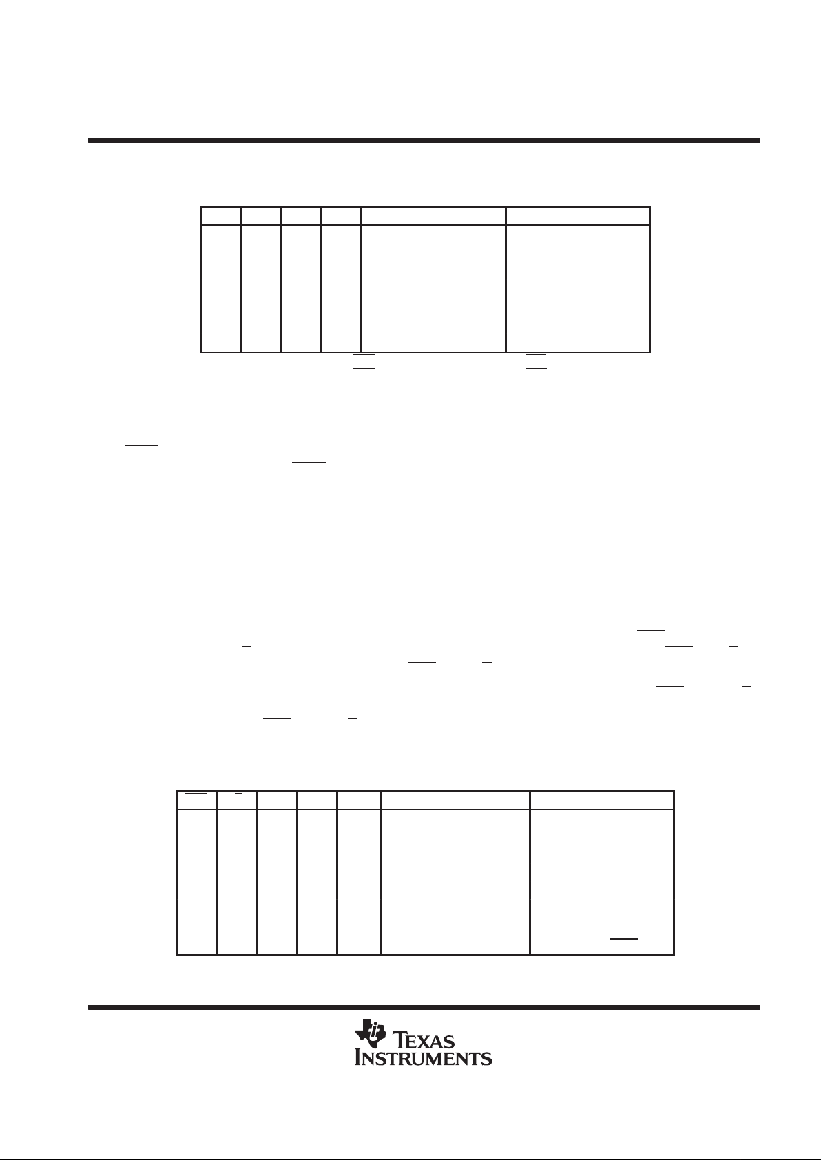
Terminal Functions (Continued)
TERMINAL
NAME
I/O DESCRIPTION
ORB
O
(port B)
Port-B output-ready flag. ORB is synchronized to the low-to-high transition of CLKB. When ORB is low, FIFO1 is empty
and reads from its memory are disabled. Ready data is present on the output register of FIFO1 when ORB is high.
ORB is forced low when FIFO1 is reset and goes high on the third low-to-high transition of CLKB after a word is loaded
to empty memory.
RDYA
O
(port A)
Port-A ready. A high on W/RA selects the inverted state of IRA for output on RDYA, and a low on W/RA selects the
inverted state of ORA for output on RDYA
.
RDYB
O
(port B)
Port-B ready. A low on W/RB selects the inverted state of IRB for output on RDYB , and a high on W/RB selects the
inverted state of ORB for output on RDYB
.
RFM I
FIFO1 read from mark. When FIFO1 is in retransmit mode, a high on RFM enables a low-to-high transition of CLKB
to reset the FIFO1 read pointer to the retransmit location and output the first retransmit data.
RST1 I
FIFO1 reset. T o reset FIFO1, four low-to-high transitions of CLKA and four low-to-high transitions of CLKB must occur
while RST1
is low. The low-to-high transition of RST1 latches the status of FS0 and FS1 for AFA and AEB offset
selection. FIFO1 must be reset upon power up before data is written to its RAM.
RST2 I
FIFO2 reset. T o reset FIFO2, four low-to-high transitions of CLKA and four low-to-high transitions of CLKB must occur
while RST2
is low. The low-to-high transition of RST2 latches the status of FS0 and FS1 for AFB and AEA offset
selection. FIFO2 must be reset upon power up before data is written to its RAM.
RTM I
FIFO1 retransmit mode. When RTM is high and valid data is present on the output of FIFO1, a low-to-high transition
of CLKB selects the data for the beginning of a FIFO1 retransmit. The selected position remains the initial retransmit
point until a low-to-high transition of CLKB occurs while RTM is low , which takes FIFO out of retransmit mode.
W/RA I
Port-A write/read select. A high on W/RA selects a write operation and a low selects a read operation on port A for
a low-to-high transition of CLKA. The A0–A31 outputs are in the high-impedance state when W/R
A is high.
W/RB I
Port-B write/read select. A low on W/RB selects a write operation and a high selects a read operation on port B for
a low-to-high transition of CLKB. The B0–B31 outputs are in the high-impedance state when W
/RB is low.
detailed description
reset
The FIFO memories of the SN74ACT3638 are reset separately by taking their reset (RST1
, RST2) inputs low
for at least four port-A clock (CLKA) and four port-B clock (CLKB) low-to-high transitions. The reset inputs can
switch asynchronously to the clocks. A FIFO reset initializes the internal read and write pointers and forces the
input-ready flag (IRA, IRB) low, the output-ready flag (ORA, ORB) low, the almost-empty flag (AEA
, AEB) low,
and the almost-full flag (AFA
, AFB) high. Resetting a FIFO also forces the mailbox flag (MBF1, MBF2) of the
parallel mailbox register high. After a FIFO is reset, its input-ready flag is set high after two clock cycles to begin
normal operation. A FIFO must be reset after power up before data is written to its memory.
A low-to-high transition on a FIFO reset (RST1
, RST2) input latches the value of the flag-select (FS0, FS1)
inputs for choosing the almost-full and almost-empty offset programming method (see
almost-empty and
almost-full flag offset programming
).
almost-empty flag and almost-full flag offset programming
Four registers in the SN74ACT3638 are used to hold the offset values for the almost-empty and almost-full flags.
The port-B almost-empty flag (AEB
) offset register is labeled X1, and the port-A almost-empty flag (AEA) offset
register is labeled X2. The port-A almost-full flag (AFA
) offset register is labeled Y1, and the port-B almost-full
flag (AFB
) offset register is labeled Y2. The index of each register name corresponds to its FIFO number . The
offset registers can be loaded with preset values during the reset of a FIFO or they can be programmed from
port A (see Table 1).
SN74ACT3638
512 × 32 × 2
CLOCKED BIDIRECTIONAL FIRST-IN, FIRST-OUT MEMORY
SCAS228D – JUNE 1992 – REVISED APRIL 1998
7
POST OFFICE BOX 655303 • DALLAS, TEXAS 75265
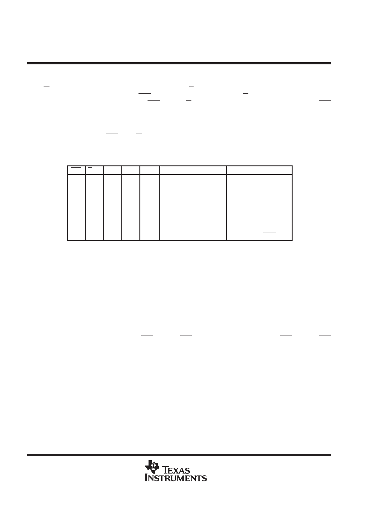
almost-empty flag and almost-full flag offset programming (continued)
T able 1. Flag Programming
FS1 FS0 RST1 RST2
X1 AND Y1 REGISTERS
†
X2 AND Y2 REGISTERS
‡
H H ↑ X 64 X
H H X ↑ X 64
H L ↑ X 16 X
H L X ↑ X 16
L H ↑ X 8 X
L H X ↑ X 8
L L ↑ ↑ Programmed from port A Programmed from port A
†
X1 register holds the offset for AEB; Y1 register holds the offset for AFA.
‡
X2 register holds the offset for AEA
; Y2 register holds the offset for AFB.
T o load the almost-empty flag and almost-full flag of fset registers of a FIFO with one of the three preset values
listed in Table 1, at least one of the flag-select inputs must be high during the low-to-high transition of its reset
input. For example, to load the preset value of 64 into X1 and Y1, FS0 and FS1 must be high when FIFO1 reset
(RST1
) returns high. Flag-offset registers associated with FIFO2 are loaded with one of the preset values in the
same way with FIFO2 reset (RST2
). When using one of the preset values for the flag offsets, the FIFOs can
be reset simultaneously or at different times.
To program the X1, X2, Y1, and Y2 registers from port A, both FIFOs should be reset simultaneously with FS0
and FS1 low during the low-to-high transition of the reset inputs. After this reset is complete, the first four writes
to FIFO1 do not store data in RAM but load the offset registers in the order Y1, X1, Y2, X2. Each offset register
uses port-A (A8–A0) inputs, with A8 as the most-significant bit. Each register value can be programmed from
1 to 508. After all the offset registers are programmed from port A, the port-B input-ready flag (IRB) is set high,
and both FIFOs begin normal operation.
FIFO write/read operation
The state of the port-A data (A0 –A31) outputs is controlled by the port-A chip select (CSA
) and the port-A
write/read select (W/R
A). The A0–A31 outputs are in the high-impedance state when either CSA or W/RA is
high. The A0–A31 outputs are active when both CSA
and W/RA are low.
Data is loaded into FIFO1 from the A0–A31 inputs on a low-to-high transition of CLKA when CSA
is low, W/RA
is high, ENA is high, MBA is low, and IRA is high. Data is read from FIFO2 to the A0–A31 outputs by a low-to-high
transition of CLKA when CSA
is low, W/RA is low , ENA is high, MBA is low , and ORA is high (see T able 2). FIFO
reads and writes on port A are independent of any concurrent port-B operation.
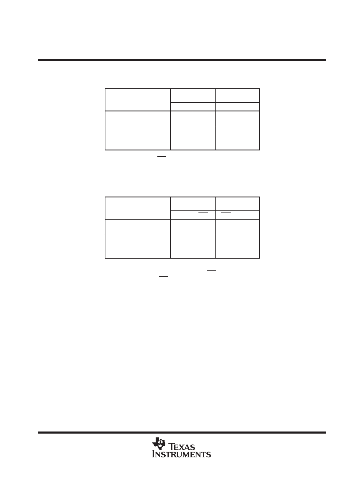
Table 2. Port-A Enable Function Table
CSA W/RA ENA MBA CLKA
A0–A31 OUTPUTS PORT FUNCTION
H X X X X In high-impedance state None
L H L X X In high-impedance state None
L H H L ↑ In high-impedance state FIFO1 write
L H H H ↑ In high-impedance state Mail1 write
L L L L X Active, FIFO2 output register None
L L H L ↑ Active, FIFO2 output register FIFO2 read
L L L H X Active, mail2 register None
L L H H ↑ Active, mail2 register Mail2 read (set MBF2 high)
SN74ACT3638
512 × 32 × 2
CLOCKED BIDIRECTIONAL FIRST-IN, FIRST-OUT MEMORY
SCAS228D – JUNE 1992 – REVISED APRIL 1998
8
POST OFFICE BOX 655303 • DALLAS, TEXAS 75265
FIFO write/read operation (continued)
The port-B control signals are identical to those of port A with the exception that the port-B write/read select
(W
/RB) is the inverse of the port-A write/read select (W/RA). The state of the port-B data (B0–B31) outputs is
controlled by the port-B chip select (CSB
) and the port-B write/read select (W/RB). The B0–B31 outputs are
in the high-impedance state when either CSB
is high or W/RB is low. The B0–B31 outputs are active when CSB
is low and W/RB is high.
Data is loaded into FIFO2 from the B0–B31 inputs on a low-to-high transition of CLKB when CSB
is low, W/RB
is low, ENB is high, MBB is low , and IRB is high. Data is read from FIFO1 to the B0–B31 outputs by a low-to-high
transition of CLKB when CSB
is low, W/RB is high, ENB is high, MBB is low , and ORB is high (see T able 3). FIFO
reads and writes on port B are independent of any concurrent port-A operation.
Table 3. Port-B Enable Function Table
CSB W/RB ENB MBB CLKB
B0–B31 OUTPUTS PORT FUNCTION
H X X X X In high-impedance state None
L L L X X In high-impedance state None
L L H L ↑ In high-impedance state FIFO2 write
L L H H ↑ In high-impedance state Mail2 write
L H L L X Active, FIFO1 output register None
L H H L ↑ Active, FIFO1 output register FIFO1 read
L H L H X Active, mail1 register None
L H H H ↑ Active, mail1 register Mail1 read (set MBF1 high)
The setup- and hold-time constraints to the port clocks for the port-chip selects and write/read selects are only
for enabling write and read operations and are not related to high-impedance control of the data outputs. If a
port enable is low during a clock cycle, the port-chip select and write/read select can change states during the
setup- and hold-time window of the cycle.
When a FIFO output-ready flag is low, the next data word is sent to the FIFO output register automatically by
the low-to-high transition of the port clock that sets the output-ready flag high. When the output-ready flag is
high, an available data word is clocked to the FIFO output register only when a FIFO read is selected by the
port-chip select, write/read select, enable, and mailbox select.
synchronized FIFO flags
Each FIFO is synchronized to its port clock through at least two flip-flop stages. This is done to improve
flag-signal reliability by reducing the probability of metastable events when CLKA and CLKB operate
asynchronously to one another. ORA, AEA
, IRA, and AFA are synchronized to CLKA. ORB, AEB, IRB, and AFB
are synchronized to CLKB. Tables 4 and 5 show the relationship of each port flag to FIFO1 and FIFO2.
SN74ACT3638
512 × 32 × 2
CLOCKED BIDIRECTIONAL FIRST-IN, FIRST-OUT MEMORY
SCAS228D – JUNE 1992 – REVISED APRIL 1998
9
POST OFFICE BOX 655303 • DALLAS, TEXAS 75265
synchronized FIFO flags (continued)
Table 4. FIFO1 Flag Operation
NUMBER OF WORDS
SYNCHRONIZED
TO CLKB
SYNCHRONIZED
TO CLKA
IN
FIFO1
†‡
ORB AEB AFA IRA
0 L L H H
1 to X1 H LHH
(X1 + 1) to [512 – (Y1 + 1)] H HHH
(512 – Y1) to 511 H HLH
512 H H L L
†
X1 is the almost-empty offset for FIFO1 used by AEB. Y1 is the almost-full
offset for FIFO1 used by AFA
. Both X1 and Y1 are selected during a reset of
FIFO1 or programmed from port A.
‡
When a word loaded to an empty FIFO is shifted to the output register, its
previous FIFO memory location is free.
Table 5. FIFO2 Flag Operation
NUMBER OF WORDS
SYNCHRONIZED
TO CLKA
SYNCHRONIZED
TO CLKB
IN
FIFO2
‡§
ORA AEA AFB IRB
0 L L H H
1 to X2 H LHH
(X2 + 1) to [512 – (Y2 +1)] H HHH
(512 – Y2) to 511 H HLH
512 H H L L
‡
When a word loaded to an empty FIFO is shifted to the output register, its
previous FIFO memory location is free.
§
X2 is the almost-empty offset for FIFO2 used by AEA
. Y2 is the almost-full
offset for FIFO2 used by AFB
. Both X2 and Y2 are selected during a reset
of FIFO2 or programmed from port A.
output-ready flags (ORA, ORB)
The output-ready flag of a FIFO is synchronized to the port clock that reads data from its array. When the
output-ready flag is high, new data is present in the FIFO output register. When the output-ready flag is low , the
previous data word is present in the FIFO output register and attempted FIFO reads are ignored.
A FIFO read pointer is incremented each time a new word is clocked to its output register. From the time a word
is written to a FIFO, it can be shifted to the FIFO output register in a minimum of three cycles of the output-ready
flag synchronizing clock; therefore, an output-ready flag is low if a word in memory is the next data to be sent
to the FIFO output register and three cycles of the port clock that reads data from the FIFO have not elapsed
since the time the word was written. The output-ready flag of the FIFO remains low until the third low-to-high
transition of the synchronizing clock occurs, simultaneously forcing the output-ready flag high and shifting the
word to the FIFO output register.
A low-to-high transition on an output-ready flag synchronizing clock begins the first synchronization cycle of a
write if the clock transition occurs at time t
sk1
, or greater, after the write. Otherwise, the subsequent clock cycle
can be the first synchronization cycle (see Figures 7 and 8).
 Loading...