


SN65LVDS22, SN65LVDM22 DUAL MULTIPLEXED LVDS REPEATERS
SLLS315± DECEMBER 1998
DMeets or Exceeds the Requirements of ANSI TIA/EIA±644±1995 Standard
DDesigned for Signaling Rates Up to 400 Mbit/s
DESD Protection Exceeds 12 kV on Bus Pins
DOperates from a Single 3.3-V Supply
DLow-Voltage Differential Signaling with Output Voltages of 350 mVinto:
±100-Ω Load (SN65LVDS22)
±50-Ω Load (SN65LVDM22)
DPropagation Delay Time; 4 ns Typ
DPower Dissipation at 400 Mbit/s of 150 mW
DBus Pins are High Impedance When Disabled or With VCC Less Than 1.5 V
D PACKAGE (TOP VIEW)
1B |
|
1 |
16 |
|
VCC |
|
|
||||
1A |
|
2 |
15 |
|
VCC |
|
|
||||
S0 |
|
3 |
14 |
|
1Y |
|
|
||||
1DE |
|
4 |
13 |
|
1Z |
|
|
||||
S1 |
|
5 |
12 |
|
2DE |
|
|
||||
2A |
|
6 |
11 |
|
2Z |
|
|
||||
2B |
|
7 |
10 |
|
2Y |
|
|
||||
GND |
|
8 |
9 |
|
GND |
|
|
||||
|
|
|
|
|
|
logic diagram (positive logic)
D LVTTL Levels are 5 V Tolerant |
|
|
1A |
2 |
|
|
|
+ |
|
|
|
|
|
|
|
|
|
|
|
|
|
|
||||
|
|
|
|
|
|
|
|
|
|
|
|
|
|
|
|
|
|
|
|
|
|
|
||||
D Open-Circuit Fail Safe Receiver |
|
|
|
|
|
|
|
|
|
|
|
|
|
|
|
14 |
|
|||||||||
|
|
|
|
|
|
|
|
|
|
|
|
|
|
|
|
|
|
|
||||||||
|
|
|
|
|
|
1B |
1 |
|
|
|
_ |
|
|
|
0 |
|
|
|
|
|
|
1Y |
||||
|
|
|
|
|
|
|
|
|
|
|
|
|
|
|
|
|
|
|||||||||
description |
|
|
|
|
|
|
|
|
|
|
|
|
|
1 |
|
|
|
|
13 |
|
||||||
|
|
|
|
|
|
|
|
|
|
|
|
|
|
|
|
|
|
|
|
|||||||
|
|
|
|
|
|
|
|
|
|
|
|
|
|
|
|
|
|
|
1Z |
|||||||
The SN65LVDS22 and SN65LVDM22 are differ- |
1DE |
4 |
|
|
|
|
|
|
|
|
|
|
|
|
|
|
|
|
|
|
||||||
|
|
|
|
|
|
|
|
|
|
|
|
|
|
|
|
|
|
|||||||||
ential line |
drivers |
and |
receivers |
that |
use |
|
|
|
|
|
|
|
|
|
|
|
|
|
|
|
|
|
|
|||
12 |
|
|
|
|
|
|
|
|
|
|
|
|
|
|
|
|
|
|
||||||||
low-voltage differential signaling (LVDS) to |
2DE |
|
|
|
|
|
|
|
|
|
|
|
|
|
|
|
|
|
|
|||||||
3 |
|
|
|
|
|
|
|
|
|
|
|
|
|
|
|
|
|
|
||||||||
achieve signaling rates as high as 400 Mbps. The |
S0 |
|
|
|
|
|
|
|
|
|
|
|
|
|
|
|
|
|
|
|||||||
receiver outputs can be switched to either or both |
|
|
|
|
|
|
|
|
|
|
|
|
|
|
|
|
|
|
|
|||||||
|
|
|
|
|
|
|
|
|
|
|
|
|
|
|
|
|
|
|
|
|
||||||
drivers through the multiplexer control signals S0 |
|
|
5 |
|
|
|
|
|
|
|
|
|
|
|
|
|
|
|
|
|
|
|||||
|
|
|
|
|
|
|
|
|
|
|
|
|
|
|
|
|
|
|
|
|||||||
and S1. This allows the flexibility to perform |
S1 |
|
|
|
|
|
|
|
|
|
|
|
|
|
|
|
|
|
|
|||||||
|
|
|
|
|
|
|
|
|
|
|
|
|
|
|
|
|
|
|
||||||||
splitter or signal routing functions with a single |
|
|
|
|
|
|
|
|
|
|
|
|
0 |
|
|
|
|
10 |
|
|
||||||
device. |
|
|
|
|
|
|
|
6 |
|
|
|
|
|
|
|
|
|
|
|
2Y |
||||||
|
|
|
|
|
|
|
|
|
|
|
|
|
|
|
|
|
|
|||||||||
|
|
|
|
|
|
|
|
|
|
|
|
|
|
|
|
|
||||||||||
|
|
|
|
|
|
2A |
|
|
|
+ |
|
|
|
|
|
|
|
|
|
|
11 |
|
||||
|
|
|
|
|
|
|
|
|
|
|
|
|
|
|
|
|
|
|
|
|||||||
|
|
|
|
|
|
|
|
|
|
|
|
|
|
|
|
|
|
|
|
|||||||
The TIA/EIA-644 standard |
compliant |
electrical |
|
|
|
|
|
|
|
|
|
|
|
|
|
2Z |
||||||||||
|
|
|
|
|
|
|
|
|
|
|
|
|
|
|
|
|
|
|
||||||||
|
|
7 |
_ |
1 |
|
|
|
|
|
|
|
|
||||||||||||||
interface provides a minimum differential output |
2B |
|
|
|
|
|
|
|
|
|||||||||||||||||
|
|
|
|
|
|
|
|
|
|
|
|
|
|
|
|
|
|
|
||||||||
voltage magnitude of 247 mV into a 100-Ω load |
|
|
|
|
|
|
|
|
|
|
|
|
|
|
|
|
|
|
|
|
|
|||||
and receipt of 100 mV signals with up to 1 V of |
|
|
|
|
|
|
|
MUX Truth Table |
|
|
|
|
|
|
||||||||||||
ground potential difference between a transmitter |
|
|
|
|
|
|
|
|
|
|
|
|
|
|||||||||||||
|
|
|
|
|
|
|
|
|
|
|
|
|
|
|
|
|
|
|
|
|
||||||
|
|
INPUT |
|
|
|
OUTPUT |
|
|
|
|
|
|
||||||||||||||
and receiver. The |
SN65LVDM22 doubles |
the |
|
|
|
|
|
FUNCTION |
||||||||||||||||||
output drive current to achieve LVDS levels with a |
|
|
S1 |
|
|
S0 |
1Y/1Z |
2Y/2Z |
||||||||||||||||||
|
|
|
|
|
|
|
|
|
|
|||||||||||||||||
50 Ω load. |
|
|
|
|
|
|
|
|
|
|
|
|
|
|
|
|||||||||||
|
|
|
|
|
|
|
|
|
|
|
|
|
|
|
|
|
|
|
|
|
|
|
|
|
|
|
|
|
|
|
|
|
|
0 |
0 |
1A/1B |
1A/1B |
|
Splitter |
||||||||||||||
|
|
|
|
|
|
|
|
|
||||||||||||||||||
The intended application of these devices and |
|
|
|
|
|
|
|
|
|
|||||||||||||||||
|
|
0 |
1 |
2A/2B |
2A/2B |
|
Splitter |
|
||||||||||||||||||
signaling technique is for both point±to±point |
|
|
1 |
0 |
1A/1B |
2A/2B |
|
Router |
|
|||||||||||||||||
baseband |
(single |
termination) and |
multipoint |
|
|
1 |
1 |
2A/2B |
1A/1B |
|
Router |
|||||||||||||||
(double termination) data transmissions over controlled impedance media. The transmission
media may be printed circuit board traces, backplanes, or cables. (Note: The ultimate rate and distance of data transfer is dependent upon the attenuation characteristics of the media, the noise coupling to the environment, and other application specific characteristics).
The SN65LVDS22 and SN65LVDM22 are characterized for operation from ±40 C to 85 C.
Please be aware that an important notice concerning availability, standard warranty, and use in critical applications of
Texas Instruments semiconductor products and disclaimers thereto appears at the end of this data sheet.
PRODUCTION DATA information is current as of publication date. Products conform to specifications per the terms of Texas Instruments standard warranty. Production processing does not necessarily include testing of all parameters.
Copyright 1998, Texas Instruments Incorporated
POST OFFICE BOX 655303 •DALLAS, TEXAS 75265 |
1 |

SN65LVDS22, SN65LVDM22
DUAL MULTIPLEXED LVDS REPEATERS
SLLS315± DECEMBER 1998
equivalent input and output schematic diagrams
VCC
VCC
300 kΩ
50 Ω |
|
S0, S1 |
|
Input |
50 Ω |
|
|
|
1DE, 2DE |
7 V |
Input |
|
|
300 kΩ |
7 V |
VCC |
VCC |
300 kΩ |
300 kΩ |
A Input |
B Input |
7 V |
7 V |
|
5 Ω |
Y or Z |
10 kΩ |
|
|
|
Output |
|
|
|
|
|
|
7 V |
2 |
POST OFFICE BOX 655303 •DALLAS, TEXAS 75265 |
SN65LVDS22, SN65LVDM22
DUAL MULTIPLEXED LVDS REPEATERS
SLLS315± DECEMBER 1998
absolute maximum ratings over operating free-air temperature (unless otherwise noted)²
Supply voltage range, VCC (see Note 1) . . . . . . . . . . . . . . . . . . . . . . . . . . . . . . . . . |
. . . . . . . . . . . . . ±0.5 V to 4 V |
Voltage range (DE, S0, S1) . . . . . . . . . . . . . . . . . . . . . . . . . . . . . . . . . . . . . . . . . . . . . |
. . . . . . . . . . . . . ±0.5 V to 6 V |
Input voltage range, VI (A or B) . . . . . . . . . . . . . . . . . . . . . . . . . . . . . . . . . . . . . . . . . |
. . . . . . . ±0.5 V to Vcc+0.5 V |
Electrostatic discharge: A, B, Y, Z and GND (see Note 2) . . . . . . . . . . . . . . . . . . |
. . Class 3, A:12 kV, B:600 V |
All pins . . . . . . . . . . . . . . . . . . . . . . . . . . . . . . . . . . . . . . . . . |
. . . Class 3, A:5 kV, B:500 V |
Continuous power dissipation . . . . . . . . . . . . . . . . . . . . . . . . . . . . . . . . . . . . . . . . . |
See Dissipation Rating Table |
Storage temperature range . . . . . . . . . . . . . . . . . . . . . . . . . . . . . . . . . . . . . . . . . . . . . |
. . . . . . . . . . . ±65°C to 150°C |
Lead temperature 1,6 mm (1/16 inch) from case for 10 seconds . . . . . . . . . . . . |
. . . . . . . . . . . . . . . . . . . 260°C |
²Stresses beyond those listed under ªabsolute maximum ratingsº may cause permanent damage to the device. These are stress ratings only, and functional operation of the device at these or any other conditions beyond those indicated under ªrecommended operating conditionsº is not implied. Exposure to absolute-maximum-rated conditions for extended periods may affect device reliability.
NOTES: 1. All voltage values, except differential I/O bus voltages, are with respect to network ground terminal. 2. Tested in accordance with MIL-STD-883C Method 3015.7.
DISSIPATION RATING TABLE
|
T |
|
≤ 25°C |
DERATING FACTOR³ |
T = 85°C |
|
PACKAGE |
A |
|
ABOVE TA = 25°C |
A |
||
POWER RATING |
POWER RATING |
|||||
|
||||||
D16 |
|
950 mW |
7.6 mW/°C |
494 mW |
||
³This is the inverse of the junction-to-ambient thermal resistance when board-mounted and with no air flow.
recommended operating conditions
|
|
|
MIN |
NOM |
MAX |
UNIT |
|||
|
|
|
|
|
|
|
|
|
|
Supply voltage, VCC |
|
3 |
3.3 |
3.6 |
V |
||||
High-level input voltage, VIH |
S0, S1, 1DE, 2DE |
2 |
|
|
|
|
V |
||
Low-level input voltage, VIL |
S0, S1, 1DE, 2DE |
|
|
|
|
0.8 |
V |
||
Magnitude of differential input voltage, VID |
|
0.1 |
|
0.6 |
V |
||||
|
|
|
VID |
|
|
VID |
|
V |
|
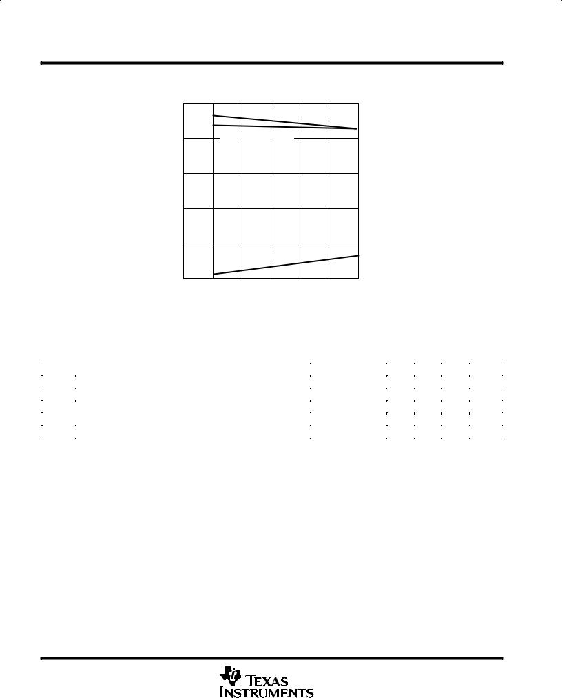
Common-mode input voltage, VIC (see Figure 1) |
|
|
|
2.4 ± 2 |
|||||
|
|
2 |
|
|
|
|
|||
|
|
|
|
|
|
VCC±0.8 |
V |
||
Operating free-air temperature, TA |
|
±40 |
|
85 |
°C |
||||
POST OFFICE BOX 655303 •DALLAS, TEXAS 75265 |
3 |
SN65LVDS22, SN65LVDM22
DUAL MULTIPLEXED LVDS REPEATERS
SLLS315± DECEMBER 1998
COMMON-MODE INPUT VOLTAGE vs
DIFFERENTIAL INPUT VOLTAGE
|
2.5 |
|
|
MAX at VCC > 3.15 V |
|
||
|
|
|
|
|
|||
± V |
|
|
MAX at VCC = 3 V |
|
|
|
|
Voltage |
2 |
|
|
|
|
||
|
|
|
|
|
|
||
|
|
|
|
|
|
|
|
-Mode Input |
1.5 |
|
|
|
|
|
|
|
|
|
|
|
|
|
|
± Common |
1 |
|
|
|
|
|
|
0.5 |
|
|
|
|
|
|
|
IC |
|
|
Min |
|
|
|
|
|
|
|
|
|
|
||
V |
|
|
|
|
|
|
|
|
|
|
|
|
|
|
|
|
0 |
|
|
|
0.4 |
0.5 |
0.6 |
|
0 |
0.1 |
0.2 |
0.3 |
|||
|
|
VID ± Differential Input Voltage ± V |
|
||||
Figure 1. Common-Mode Input Voltage vs Differential Input Voltage
receiver electrical characteristics over recommended operating conditions (unless otherwise noted)
|
PARAMETER |
TEST CONDITIONS |
MIN TYP² |
MAX |
UNIT |
VITH+ |
Positive-going differential input voltage threshold |
|
|
100 |
mV |
VITH± |
Negative-going differential input voltage threshold |
|
±100 |
|
mV |
II |
Input current (A or B inputs) |
VI = 0 V |
±2 |
±20 |
μA |
VI = 2.4 V |
±1.2 |
|
|||
|
|
|
|
||
II(OFF) |
Power-off input current (A or B inputs) |
VCC = 0 V |
|
20 |
μA |
4 |
POST OFFICE BOX 655303 •DALLAS, TEXAS 75265 |
 Loading...