Texas Instruments SN74ACT1284DBLE, SN74ACT1284DBR, SN74ACT1284DW, SN74ACT1284DWR, SN74ACT1284PWR Datasheet

SN54ACT1284, SN74ACT1284 7-BIT BUS INTERFACES WITH 3-STATE OUTPUTS
SCAS459B ± NOVEMBER 1994 ± REVISED APRIL 1996
D D
3-State Outputs Directly Drive Bus Lines
Flow-Through Architecture Optimizes PCB
Layout
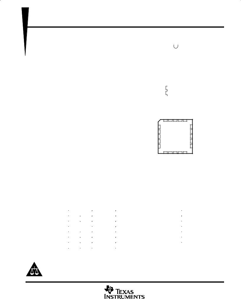
SN54ACT1284 . . . J OR W PACKAGE SN74ACT1284 . . . DB, DW, N, OR PW PACKAGE (TOP VIEW)
DCenter-Pin VCC and GND Configurations Minimize High-Speed Switching Noise
DESD Protection Exceeds 2000 V Per MIL-STD-883, Method 3015; Exceeds 200 V Using Machine Model (C = 200 pF, R = 0)
DDesigned for the IEEE 1284-I (Level 1 Type) and IEEE 1284-II (Level 2 Type) Electrical Specifications
DPackage Options Include Plastic Small-Outline (DW), Shrink Small-Outline (DB), Thin Shrink Small-Outline (PW), and DIP (N) Packages, Ceramic Chip Carriers (FK), Flat (W), and DIP (J) Packages
A1 |
|
1 |
20 |
|
B1 |
|
|
||||
A2 |
|
2 |
19 |
|
B2 |
|
|
||||
A3 |
|
3 |
18 |
|
B3 |
|
|
||||
A4 |
|
4 |
17 |
|
B4 |
|
|
||||
GND |
|
5 |
16 |
|
VCC |
|
|
||||
|
|
||||
GND |
|
6 |
15 |
|
VCC |
A5 |
|
|
|||
|
7 |
14 |
|
B5 |
|
A6 |
|
8 |
13 |
|
B6 |
|
|
||||
A7 |
9 |
12 |
|
B7 |
|
|
|||||
DIR |
10 |
11 |
|
HD |
|
|
|||||
|
|
|
|
|
|
FK PACKAGE (TOP VIEW)
description
The 'ACT1284 are designed for asynchronous two-way communication between data buses. The control function minimizes external timing requirements.
The devices allow data transmission in either the A-to-B or the B-to-A direction for bits 1, 2, 3, and 4, depending on the logic level at the direction-control (DIR) input. Bits 5, 6, and 7, however, always transmit in the A-to-B direction.
|
A3 |
A2 |
A1 |
B1 |
B2 |
|
A4 |
3 |
2 |
1 |
20 19 |
B3 |
|
4 |
|
|
|
18 |
||
GND |
5 |
|
|
|
17 |
B4 |
GND |
6 |
|
|
|
16 |
VCC |
A5 |
7 |
|
|
|
15 |
VCC |
A6 |
8 |
|
|
|
14 |
B5 |
|
9 |
10 11 12 13 |
|
|||
|
A7 |
DIR |
HD |
B7 |
B6 |
|
The output drive for each mode is determined by the high drive (HD) control pin. When HD is high, the high drive is delivered by the totem-pole configuration, and when HD is low, the outputs are open drain. This meets the drive requirements as specified in the IEEE 1284-I (level 1 type) and the IEEE 1284-II (level 2 type) parallel peripheral-interface specification.
The SN54ACT1284 is characterized for operation over the full military temperature range of ±55°C to 125°C. The SN74ACT1284 is characterized for operation from 0°C to 70°C.
FUNCTION TABLE
INPUTS |
OUTPUT |
MODE |
||
|
|
|||
DIR |
HD |
|||
|
|
|||
|
|
|
|
|
L |
L |
Open drain |
A to B: Bits 5, 6, 7 |
|
|
|
|||
Totem pole |
B to A: Bits 1, 2, 3, 4 |
|||
|
|
|||
|
|
|
|
|
L |
H |
Totem pole |
B to A: Bits 1, 2, 3, 4 and A to B: Bits 5, 6, 7 |
|
|
|
|
|
|
H |
L |
Open drain |
A to B: Bits 1, 2, 3, 4, 5, 6, 7 |
|
|
|
|
|
|
H |
H |
Totem pole |
A to B: Bits 1, 2, 3, 4, 5, 6, 7 |
|
|
|
|
|
|
Please be aware that an important notice concerning availability, standard warranty, and use in critical applications of Texas Instruments semiconductor products and disclaimers thereto appears at the end of this data sheet.
UNLESS OTHERWISE NOTED this document contains PRODUCTION DATA information current as of publication date. Products conform to specifications per the terms of Texas Instruments standard warranty. Production processing does not necessarily include testing of all parameters.
Copyright 1996, Texas Instruments Incorporated
POST OFFICE BOX 655303 •DALLAS, TEXAS 75265 |
1 |

SN54ACT1284, SN74ACT1284 7-BIT BUS INTERFACES WITH 3-STATE OUTPUTS
SCAS459B ± NOVEMBER 1994 ± REVISED APRIL 1996
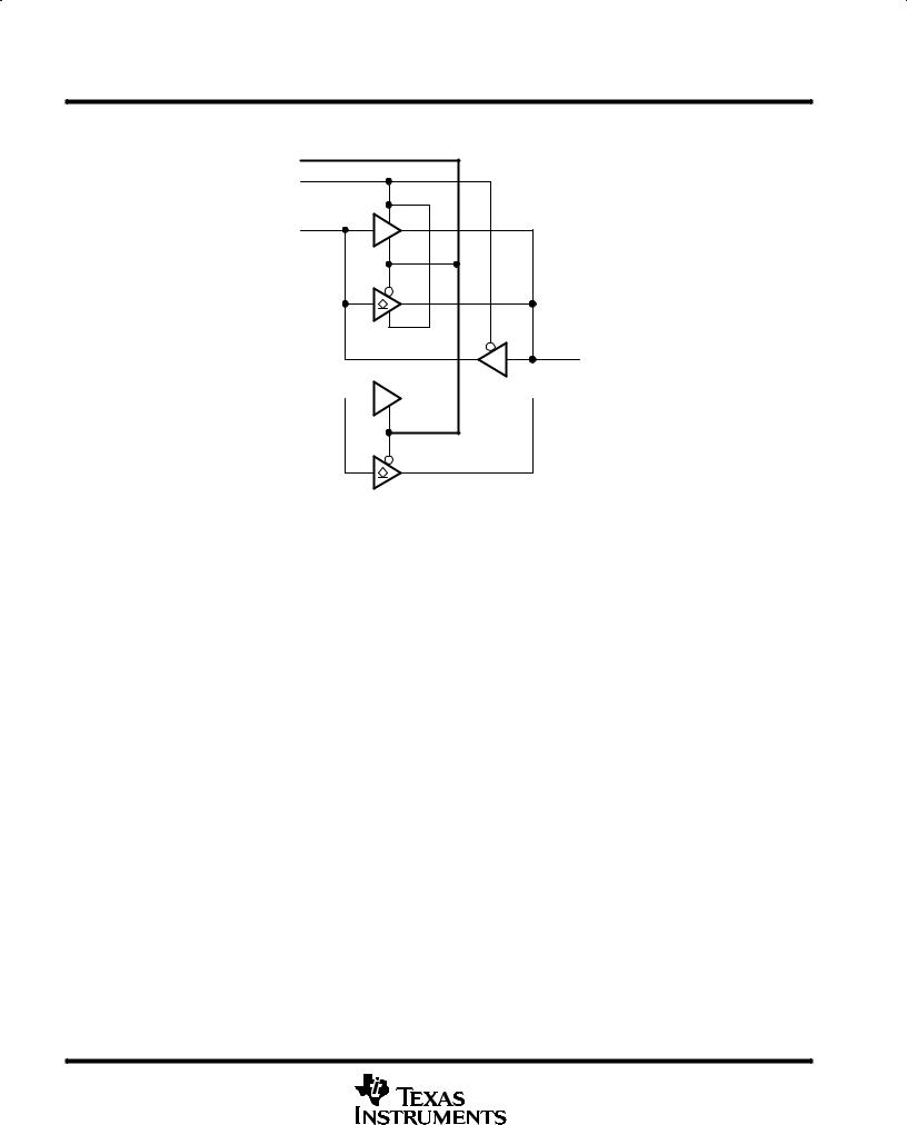
logic diagram (positive logic)
HD
DIR
A1, A2, A3, A4
B1, B2, B3, B4
A5, A6, A7  B5, B6, B7
absolute maximum ratings over operating free-air temperature range (unless otherwise noted)²
Supply voltage range, VCC . . . . . . . . . . . . . . . . . . . . . . . . . . . . . . . . . . . . . . . . . . . . . . . . . . . |
. . . . . . . ±0.5 V to 7 |
V |
B-port input and output voltage range, VI and VO (see Notes 1 and 2) . . . . . . . . . . . . . . |
. . . . . . . . ±2 V to 7 |
V |
A-port input and output voltage range, VI and VO (see Note 1) . . . . . . . . . . . . . . . . . . . . |
±0.5 V to VCC + 0.5 |
V |
Input clamp current, IIK (VI < 0 or VI > VCC) . . . . . . . . . . . . . . . . . . . . . . . . . . . . . . . . . . . . . |
. . . . . . . . . . . ±20 mA |
|
Output clamp current, IOK (VO < 0 or VO > VCC) . . . . . . . . . . . . . . . . . . . . . . . . . . . . . . . . . |
. . . . . . . . . . . ±50 mA |
|
Continuous output current, IO (VO = 0 to VCC) . . . . . . . . . . . . . . . . . . . . . . . . . . . . . . . . . . . |
. . . . . . . . . . . ±50 mA |
|
Continuous current through VCC or GND . . . . . . . . . . . . . . . . . . . . . . . . . . . . . . . . . . . . . . . . |
. . . . . . . . . ±200 mA |
|
Package thermal impedance, θJA (see Note 3): DB package . . . . . . . . . . . . . . . . . . . . . . |
. . . . . . . . . . 115°C/W |
|
DW package . . . . . . . . . . . . . . . . . . . . . . |
. . . . . . . . . . . 97°C/W |
|
N package . . . . . . . . . . . . . . . . . . . . . . . . |
. . . . . . . . . . . 67°C/W |
|
PW package . . . . . . . . . . . . . . . . . . . . . . |
. . . . . . . . . . 128°C/W |
|
Storage temperature range, Tstg . . . . . . . . . . . . . . . . . . . . . . . . . . . . . . . . . . . . . . . . . . . . . . . |
. . . ±65°C to 150°C |
|
² Stresses beyond those listed under ªabsolute maximum ratingsº may cause permanent damage to the device. These are stress ratings only, and functional operation of the device at these or any other conditions beyond those indicated under ªrecommended operating conditionsº is not implied. Exposure to absolute-maximum-rated conditions for extended periods may affect device reliability.
NOTES: 1. The input and output voltage ratings may be exceeded if the input and output current ratings are observed.
2.The ac input voltage pulsewidth is limited to 20 ns if the input voltage goes more negative than ±0.5 V.
3.The package thermal impedance is calculated in accordance with JESD 51, except for through-hole packages, which use a trace length of zero.
2 |
POST OFFICE BOX 655303 •DALLAS, TEXAS 75265 |
 Loading...