


 Loading...
Analog Devices AD7890SQ-4, AD7890SQ-2, AD7890SQ-10, AD7890BR-4, AD7890BR-2 Datasheet
...
a |
LC2MOS 8-Channel, 12-Bit |
||
Serial, Data Acquisition System |
|||
|
|
|
|
|
|
AD7890 |
|
|
|
|
|
FEATURES
Fast 12-Bit ADC with 5.9 s Conversion Time
Eight Single-Ended Analog Input Channels Selection of Input Ranges:
10 V for AD7890-10
0V to 4.096 V for AD7890-4
0V to 2.5 V for AD7890-2
Allows Separate Access to Multiplexer and ADC On-Chip Track/Hold Amplifier
On-Chip Reference
High-Speed, Flexible, Serial Interface
Single Supply, Low-Power Operation (50 mW Max) Power-Down Mode (75 W Typ)
GENERAL DESCRIPTION
The AD7890 is an eight-channel 12-bit data acquisition system. The part contains an input multiplexer, an on-chip track/hold amplifier, a high-speed 12-bit ADC, a 2.5 V reference and a high speed, serial interface. The part operates from a single 5 V supply and accepts an analog input range of ±10 V (AD7890-10), 0 V to 4.096 V (AD7890-4) and 0 V to 2.5 V (AD7890-2).
The multiplexer on the part is independently accessible. This allows the user to insert an antialiasing filter or signal conditioning, if required, between the multiplexer and the ADC. This means that one antialiasing filter can be used for all eight channels. Connection of an external capacitor allows the user to adjust the time given to the multiplexer settling to include any external delays in the filter or signal conditioning circuitry.
Output data from the AD7890 is provided via a high-speed bidirectional serial interface port. The part contains an on-chip control register, allowing control of channel selection, conversion start and power-down via the serial port. Versatile, high speed logic ensures easy interfacing to serial ports on microcontrollers and digital signal processors.
In addition to the traditional dc accuracy specifications such as linearity, full-scale and offset errors, the AD7890 is also specified for dynamic performance parameters including harmonic distortion and signal-to-noise ratio.
FUNCTIONAL BLOCK DIAGRAM
VDD |
MUX SHA |
REF OUT/ |
OUT IN |
REF IN |
VIN1 |
SIGNAL |
2k |
2.5V |
SCALING* |
|
||
|
|
|
REFERENCE |
VIN2 |
SIGNAL |
|
|
SCALING* |
|
|
|
VIN3 |
SIGNAL |
|
|
SCALING* |
|
CEXT |
|
|
SIGNAL |
|
|
VIN4 |
|
|
|
SCALING* |
MUX |
|
|
|
SIGNAL |
|
|
VIN5 |
|
|
|
SCALING* |
|
|
|
VIN6 |
SIGNAL |
|
CONVST |
|
|
||
SCALING* |
12-BIT |
||
VIN7 |
SIGNAL |
|
ADC |
|
|
||
SCALING* |
|
|
|
VIN8 |
SIGNAL |
TRACK/HOLD |
|
SCALING* |
|
|
|
|
|
OUTPUT/CONTROL REGISTER |
|
|
AD7890 |
CLOCK |
|
AGND AGND DGND CLK |
SCLK TFS RFS DATA DATA SMODE |
IN |
OUT IN |
|
*NO SCALING ON AD7890-2 |
Power dissipation in normal mode is low at 30 mW typ and the part can be placed in a standby (power-down) mode if it is not required to perform conversions. The AD7890 is fabricated in Analog Devices’ Linear Compatible CMOS (LC2MOS) process, a mixed technology process that combines precision bipolar circuits with low power CMOS logic. The part is available in a 24-lead, 0.3" wide, plastic or hermetic dual-in-line package or in a 24-lead small outline package (SOIC).
PRODUCT HIGHLIGHTS
1.Complete 12-Bit Data Acquisition System-on-a-Chip
The AD7890 is a complete monolithic ADC combining an eight-channel multiplexer, 12-bit ADC, 2.5 V reference and a track/hold amplifier on a single chip.
2.Separate Access to Multiplexer and ADC
The AD7890 provides access to the output of the multiplexer allowing one antialiasing filter for eight channels—a considerable saving over the eight antialiasing filters required if the multiplexer was internally connected to the ADC.
3.High-Speed Serial Interface
The part provides a high-speed serial interface for easy connection to serial ports of microcontrollers and DSP processors.
REV. B
Information furnished by Analog Devices is believed to be accurate and reliable. However, no responsibility is assumed by Analog Devices for its use, nor for any infringements of patents or other rights of third parties which may result from its use. No license is granted by implication or otherwise under any patent or patent rights of Analog Devices.
One Technology Way, P.O. Box 9106, Norwood, MA 02062-9106, U.S.A.
Tel: 781/329-4700 |
World Wide Web Site: http://www.analog.com |
Fax: 781/326-8703 |
© Analog Devices, Inc., 2001 |
|
|
(VDD = 5 V, AGND = DGND = 0 V, REF IN = 2.5 V, fCLK IN = 2.5 MHz external, MUX OUT |
|||
AD7890–SPECIFICATIONS connect to SHA IN. All specifications TMIN to TMAX unless otherwise noted.) |
|||||
Parameter |
A Versions1 |
B Versions |
S Version |
Unit |
Test Conditions/Comments |
DYNAMIC PERFORMANCE |
|
|
|
|
Using External CONVST. Any Channel |
Signal to (Noise + Distortion) Ratio2 |
70 |
70 |
70 |
dB min |
fIN = 10 kHz Sine Wave, fSAMPLE = 100 kHz3 |
Total Harmonic Distortion (THD)2 |
–78 |
–78 |
–78 |
dB max |
fIN = 10 kHz Sine Wave, fSAMPLE = 100 kHz3 |
Peak Harmonic or Spurious Noise2 |
–79 |
–79 |
–79 |
dB max |
fIN = 10 kHz Sine Wave, fSAMPLE = 100 kHz3 |
Intermodulation Distortion |
|
|
|
|
fa = 9 kHz, fb = 9.5 kHz, fSAMPLE = 100 kHz3 |
2nd Order Terms |
–80 |
–80 |
–80 |
dB typ |
|
3rd Order Terms |
–80 |
–80 |
–80 |
dB typ |
|
Channel-to-Channel Isolation2 |
–80 |
–80 |
–80 |
dB max |
fIN = 1 kHz Sine Wave |
DC ACCURACY |
|
|
|
|
|
Resolution |
12 |
12 |
12 |
Bits |
|
Minimum Resolution for Which |
|
|
|
|
|
No Missing Codes Are Guaranteed |
12 |
12 |
12 |
Bits |
|
Relative Accuracy2 |
±1 |
±0.5 |
±1 |
LSB max |
|
Differential Nonlinearity2 |
±1 |
±1 |
±1 |
LSB max |
|
Positive Full-Scale Error2 |
±2.5 |
±2.5 |
±2.5 |
LSB max |
|
Full-Scale Error Match4 |
2 |
2 |
2 |
LSB max |
|
AD7890-2, AD7890-4 |
±2 |
±2 |
±2 |
|
|
Unipolar Offset Error2 |
LSB max |
|
|||
Unipolar Offset Error Match |
2 |
2 |
2 |
LSB max |
|
AD7890-10 Only |
±2 |
±2 |
±2 |
|
|
Negative Full-Scale Error2 |
LSB max |
|
|||
Bipolar Zero Error2 |
±5 |
±5 |
±5 |
LSB max |
|
Bipolar Zero Error Match |
2 |
2 |
2 |
LSB max |
|
|
|
|
|
|
|
ANALOG INPUTS |
|
|
|
|
|
AD7890-10 |
±10 |
±10 |
±10 |
|
|
Input Voltage Range |
Volts |
|
|||
Input Resistance |
20 |
20 |
20 |
kΩ min |
|
AD7890-4 |
|
|
|
|
|
Input Voltage Range |
0 to 4.096 |
0 to 4.096 |
0 to 4.096 |
Volts |
|
Input Resistance |
11 |
11 |
11 |
kΩ min |
|
AD7890-2 |
|
|
|
|
|
Input Voltage Range |
0 to 2.5 |
0 to 2.5 |
0 to 2.5 |
Volts |
|
Input Current |
50 |
50 |
200 |
nA max |
|
|
|
|
|
|
|
MUX OUT OUTPUT |
|
|
|
|
|
Output Voltage Range |
0 to 2.5 |
0 to 2.5 |
0 to 2.5 |
Volts |
|
Output Resistance |
|
|
|
kΩ min/kΩ max |
|
(AD7890-10, AD7890-4) |
3/5 |
3/5 |
3/5 |
|
|
(AD7890-2) |
2 |
2 |
2 |
kΩ max |
Assuming VIN Is Driven from Low Impedance |
SHA IN INPUT |
|
|
|
|
|
Input Voltage Range |
0 to 2.5 |
0 to 2.5 |
0 to 2.5 |
Volts |
|
Input Current |
±50 |
±50 |
±50 |
nA max |
|
|
|
|
|
|
|
REFERENCE OUTPUT/INPUT |
|
|
|
|
2.5 V ± 5% |
REF IN Input Voltage Range |
2.375/2.625 |
2.375/2.625 |
2.375/2.625 |
V min/V max |
|
Input Impedance |
1.6 |
1.6 |
1.6 |
kΩ min |
Resistor Connected to Internal Reference Node |
Input Capacitance5 |
10 |
10 |
10 |
pF max |
|
REF OUT Output Voltage |
2.5 |
2.5 |
2.5 |
V nom |
|
REF OUT Error @ 25°C |
±10 |
±10 |
±10 |
mV max |
|
TMIN to TMAX |
±20 |
±20 |
±25 |
mV max |
|
REF OUT Temperature Coefficient |
25 |
25 |
25 |
ppm/°C typ |
|
REF OUT Output Impedance |
2 |
2 |
2 |
kΩ nom |
|
|
|
|
|
|
|
LOGIC INPUTS |
|
|
|
|
VDD = 5 V ± 5% |
Input High Voltage, VINH |
2.4 |
2.4 |
2.4 |
V min |
|
Input Low Voltage, VINL |
0.8 |
0.8 |
0.8 |
V max |
VDD = 5 V ± 5% |
Input Current, IIN |
±10 |
±10 |
±10 |
µA max |
VIN = 0 V to VDD |
Input Capacitance, CIN5 |
10 |
10 |
10 |
pF max |
|
–2– |
REV. B |

AD7890
Parameter |
A Versions1 |
B Versions |
S Version |
Unit |
Test Conditions/Comments |
|
LOGIC OUTPUTS |
|
|
|
|
|
ISOURCE = 200 A |
Output High Voltage, VOH |
4.0 |
4.0 |
|
4.0 |
V min |
|
Output Low Voltage, VOL |
0.4 |
0.4 |
|
0.4 |
V max |
ISINK = 1.6 mA |
Serial Data Output Coding |
|
|
|
|
|
|
AD7890-10 |
|
Two’s Complement |
|
|
||
AD7890-4 |
Straight (Natural) Binary |
|
|
|||
AD7890-2 |
Straight (Natural) Binary |
|
|
|||
|
|
|
|
|
|
|
CONVERSION RATE |
|
|
|
|
s max |
|
Conversion Time |
5.9 |
5.9 |
|
5.9 |
fCLK IN = 2.5 MHz, MUX OUT |
|
Track/Hold Acquisition Time2, 5 |
|
|
|
|
s max |
Connected to SHA IN |
2 |
2 |
|
2 |
|
||
POWER REQUIREMENTS |
|
|
|
|
|
±5% for Specified Performance |
VDD |
5 |
5 |
|
5 |
V nom |
|
IDD (Normal Mode) |
10 |
10 |
|
10 |
mA max |
Logic Inputs = 0 V or VDD |
IDD (Standby Mode)6 @ 25°C |
15 |
15 |
|
15 |
A typ |
Logic Inputs = 0 V or VDD |
Power Dissipation |
|
|
|
|
|
|
Normal Mode |
50 |
50 |
|
50 |
mW max |
Typically 30 mW |
Standby Mode @ 25°C |
75 |
75 |
|
75 |
W typ |
|
NOTES
1Temperature ranges are as follows: A, B Versions: –40°C to +85°C; S Version: –55°C to +125°C. 2See Terminology.
3This sample rate is only achievable when tiling the part in external clocking mode.
4Full-scale error match applies to positive full scale for the AD7890-2 and AD7890-4. It applies to both positive and negative full scale for the AD7890-10. 5Sample tested @ 25°C to ensure compliance.
6Analog inputs on AD7890-10 must be at 0 V to achieve correct power-down current.
Specifications subject to change without notice.
ABSOLUTE MAXIMUM RATINGS* |
|
*Stresses above those listed under Absolute Maximum Ratings may cause perma- |
|||||||||||
(TA = 25°C unless otherwise noted) |
|
nent damage to the device. This is a stress rating only; functional operation of the |
|||||||||||
VDD to AGND |
–0.3 V to +7 V |
device at these or any other conditions above those listed in the operational |
|||||||||||
sections of this specification is not implied. Exposure to absolute maximum rating |
|||||||||||||
VDD to DGND . . . . . . . . . . . . . . . . . . . . |
. . . . . –0.3 V to +7 V |
conditions for extended periods may affect device reliability. |
|
|
|||||||||
Analog Input Voltage to AGND |
±17 V |
|
ORDERING GUIDE |
|
|
||||||||
|
AD7890-10, AD7890-4 |
|
|
|
|||||||||
|
|
|
|
|
|
|
|
|
|
||||
|
. . . . . . . . . . . . . . . . . . . . .AD7890-2 |
. . . . . . . –5 V, +10 V |
|
Temperature |
|
Linearity |
Package |
||||||
Reference Input Voltage to AGND . . . |
–0.3 V to VDD + 0.3 V |
Model |
Range |
|
Error |
Option* |
|||||||
Digital Input Voltage to DGND . . . . . |
–0.3 V to VDD + 0.3 V |
|
|
|
|
|
|
|
|
|
|||
AD7890AN-2 |
–40°C to +85°C |
±1 LSB |
N-24 |
||||||||||
Digital Output Voltage to DGND . . . . |
–0.3 V to VDD + 0.3 V |
||||||||||||
AD7890BN-2 |
–40°C to +85°C |
±1/2 LSB |
N-24 |
||||||||||
Operating Temperature Range |
–40°C to +85°C |
AD7890AR-2 |
–40°C to +85°C |
±1 LSB |
R-24 |
||||||||
|
Commercial (A, B Versions) . . . . . . . |
AD7890BR-2 |
–40°C to +85°C |
±1/2 LSB |
R-24 |
||||||||
|
Extended (S Version) . . . . . . . . . . . . . |
. . . –55°C to +125°C |
AD7890SQ-2 |
–55°C to +125°C |
±1 LSB |
Q-24 |
|||||||
|
Storage Temperature Range . . . . . . . . |
. . . –65°C to +150°C |
AD7890AN-4 |
–40°C to +85°C |
±1 LSB |
N-24 |
|||||||
Junction Temperature . . . . . . . . . . . . . . |
. . . . . . . . . . . . 150°C |
AD7890BN-4 |
–40°C to +85°C |
±1/2 LSB |
N-24 |
||||||||
Plastic DIP Package, Power Dissipation |
. . . . . . . . . . 450 mW |
AD7890AR-4 |
–40°C to +85°C |
±1 LSB |
R-24 |
||||||||
|
θJA Thermal Impedance . . . . . . . . . . . |
. . . . . . . . . 105°C/W |
AD7890BR-4 |
–40°C to +85°C |
±1/2 LSB |
R-24 |
|||||||
|
Lead Temperature (Soldering, 10 sec) |
260°C |
AD7890SQ-4 |
–55°C to +125°C |
±1 LSB |
Q-24 |
|||||||
|
AD7890AN-10 |
–40°C to +85°C |
±1 LSB |
N-24 |
|||||||||
Cerdip Package, Power Dissipation |
450 mW |
||||||||||||
AD7890BN-10 |
–40°C to +85°C |
±1/2 LSB |
N-24 |
||||||||||
|
θJA Thermal Impedance |
70°C/W |
|||||||||||
|
AD7890AR-10 |
–40°C to +85°C |
±1 LSB |
R-24 |
|||||||||
|
Lead Temperature (Soldering, 10 sec) |
300°C |
|||||||||||
|
AD7890BR-10 |
–40°C to +85°C |
±1/2 LSB |
R-24 |
|||||||||
SOIC Package, Power Dissipation . . . . . |
. . . . . . . . . . 450 mW |
AD7890SQ-10 |
–55°C to +125°C |
±1 LSB |
Q-24 |
||||||||
|
θJA Thermal Impedance . . . . . . . . . . . |
. . . . . . . . . . 75°C/W |
|
|
|
|
|
|
|
|
|
||
|
*N = Plastic DIP; Q = Cerdip; R = SOIC. |
|
|
|
|||||||||
|
Lead Temperature, Soldering |
215°C |
|
|
|
||||||||
|
Vapor Phase (60 sec) . . . . . . . . . . . |
|
|
|
|
|
|
|
|
|
|||
|
Infrared (15 sec) . . . . . . . . . . . . . . . |
. . . . . . . . . . . . 220°C |
|
|
|
|
|
|
|
|
|
||
|
CAUTION |
|
|
|
|
|
|
|
|
|
|
|
|
|
|
|
|
|
|
|
|
|
|
|
|
||
|
ESD (electrostatic discharge) sensitive device. Electrostatic charges as high as 4000 V readily |
|
|
|
|
|
|||||||
|
|
WARNING! |
|
|
|||||||||
|
accumulate on the human body and test equipment and can discharge without detection. |
|
|
|
|||||||||
|
Although the AD7890 features proprietary ESD protection circuitry, permanent damage may |
|
|
|
|
|
|||||||
|
occur on devices subjected to high-energy electrostatic discharges. Therefore, proper ESD |
|
|
ESD SENSITIVE DEVICE |
|
||||||||
|
precautions are recommended to avoid performance degradation or loss of functionality. |
|
|
|
|||||||||
|
|
|
|
|
|
||||||||
|
|
|
|
|
|
||||||||
|
|
|
|
|
|
|
|
|
|
|
|
|
|
REV. B |
–3– |
AD7890
TIMING CHARACTERISTICS1, 2
(VDD = 5 V 5%, AGND = DGND = 0 V, REF IN = 2.5 V, fCLK IN = 2.5 MHz external, MUX OUT connected to SHA IN.)
|
Limit at TMIN, TMAX |
|
|
Parameter |
(A, B, S Versions) |
Unit |
Conditions/Comments |
|
|
|
|
3 |
100 |
kHz min |
Master Clock Frequency. For Specified Performance |
fCLKIN |
|||
|
2.5 |
MHz max |
|
tCLK IN LO |
0.3 × tCLK IN |
ns min |
Master Clock Input Low Time |
tCLK IN HI |
0 3 × tCLK IN |
ns min |
Master Clock Input High Time |
tr4 |
25 |
ns max |
Digital Output Rise Time. Typically 10 ns |
tf4 |
25 |
ns max |
Digital Output Fall Time. Typically 10 ns |
tCONVERT |
5.9 |
µs max |
Conversion Time |
tCST |
100 |
ns min |
CONVST Pulsewidth |
Self-Clocking Mode |
|
|
|
t1 |
tCLK IN HI + 50 |
ns max |
RFS Low to SCLK Falling Edge |
t25 |
25 |
ns max |
RFS Low to Data Valid Delay |
t3 |
tCLK IN HI |
ns nom |
SCLK High Pulsewidth |
t4 |
tCLK IN LO |
ns nom |
SCLK Low Pulsewidth |
t55 |
20 |
ns max |
SCLK Rising Edge to Data Valid Delay |
t6 |
40 |
ns max |
SCLK Rising Edge to RFS Delay |
t76 |
50 |
ns max |
Bus Relinquish Time after Rising Edge of SCLK |
t8 |
0 |
ns min |
TFS Low to SCLK Falling Edge |
|
tCLK IN + 50 |
ns max |
|
t9 |
0 |
ns min |
Data Valid to TFS Falling Edge Setup Time (A2 Address Bit) |
t10 |
20 |
ns min |
Data Valid to SCLK Falling Edge Setup Time |
t11 |
10 |
ns min |
Data Valid to SCLK Falling Edge Hold Time |
t12 |
20 |
ns min |
TFS to SCLK Falling Edge Hold Time |
External-Clocking Mode |
|
|
|
t13 |
20 |
ns min |
RFS Low to SCLK Falling Edge Setup Time |
t145 |
40 |
ns max |
RFS Low to Data Valid Delay |
t15 |
50 |
ns min |
SCLK High Pulsewidth |
t16 |
50 |
ns min |
SCLK Low Pulsewidth |
t175 |
35 |
ns max |
SCLK Rising Edge to Data Valid Delay |
t18 |
20 |
ns min |
RFS to SCLK Falling Edge Hold Time |
t196 |
50 |
ns max |
Bus Relinquish Time after Rising Edge of RFS |
6 |
90 |
ns max |
Bus Relinquish Time after Rising Edge of SCLK |
t19A |
|||
t20 |
20 |
ns min |
TFS Low to SCLK Falling Edge Setup Time |
t21 |
10 |
ns min |
Data Valid to SCLK Falling Edge Setup Time |
t22 |
15 |
ns min |
Data Valid to SCLK Falling Edge Hold Time |
t23 |
40 |
ns min |
TFS to SCLK Falling Edge Hold Time |
NOTES
1Sample tested at –25°C to ensure compliance. All input signals are specified with tr = tf = 5 ns (10% to 90% of 5 V) and timed from a voltage level of 1.6 V. 2See Figures 8 to 11.
3The AD7890 is production tested with fCLK IN at 2.5 MHz. It is guaranteed by characterization to operate at 100 kHz. 4Specified using 10% and 90% points on waveform of interest.
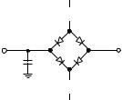
5These numbers are measured with the load circuit of Figure 1 and defined as the time required for the output to cross 0.8 V or 2.4 V.
6These numbers are derived from the measured time taken by the data output to change 0.5 V when loaded with the circuit of Figure 1. The measured number is then extrapolated back to remove effects of charging or discharging the 50 pF capacitor. This means that the times quoted in the tim ing characteristics are the true bus relinquish times of the part and as such are independent of external bus loading capacitances.
 1.6mA
1.6mA
TO OUTPUT |
+2.1V |
PIN |
50pF |
|
 200 A
200 A
Figure 1. Load Circuit for Access Time and Bus Relinquish Time
–4– |
REV. B |
|
|
AD7890 |
|
|
|
|
|
PIN FUNCTION DESCRIPTIONS |
|
|
|
Pin |
Mnemonic |
Description |
|
|
|
1 |
AGND |
Analog Ground. Ground reference for track/hold, comparator and DAC. |
2 |
SMODE |
Control Input. Determines whether the part operates in its External Clocking (slave) or Self-Clocking |
|
|
(master) serial mode. With SMODE at a logic low, the part is in its Self-Clocking serial mode with |
|
|
RFS and SCLK as outputs. This Self-Clocking mode is useful for connection to shift registers or to |
|
|
serial ports of DSP processors. With SMODE at a logic high, the part is in its External Clocking |
|
|
serial mode with SCLK and RFS as inputs. This External Clocking mode is useful for connection to |
|
|
the serial port of microcontrollers such as the 8xC51 and the 68HCxx and for connection to the |
|
|
serial ports of DSP processors. |
3 |
DGND |
Digital Ground. Ground reference for digital circuitry. |
4 |
CEXT |
External Capacitor. An external capacitor is connected to this pin to determine the length of the |
|
|
internal pulse (see CONVST input and Control Register section). Larger capacitances on this pin |
|
|
extend the pulse to allow for settling time delays through an external antialiasing filter or signal |
|
|
conditioning circuitry. |
5 |
CONVST |
Convert Start. Edge-triggered logic input. A low to high transition on this input puts the track/hold |
|
|
into hold and initiates conversion provided that the internal pulse has timed out (see Control |
|
|
Register section). If the internal pulse is active when the CONVST goes high, the track/hold will not |
|
|
go into hold until the pulse times out. If the internal pulse has timed out when CONVST goes high, |
|
|
the rising edge of CONVST drives the track/hold into hold and initiates conversion. |
6 |
CLK IN |
Clock Input. An external TTL-compatible clock is applied to this input pin to provide the clock source |
|
|
for the conversion sequence. In the Self-Clocking serial mode, the SCLK output is derived from this |
|
|
CLK IN pin. |
7 |
SCLK |
Serial Clock Input. In the External Clocking (slave) mode (see Serial Interface section) this is an |
|
|
externally applied serial clock which is used to load serial data to the control register and to access |
|
|
data from the output register. In the Self-Clocking (master) mode, the internal serial clock, which is |
|
|
derived from the clock input (CLK IN), appears on this pin. Once again, it is used to load serial data |
|
|
to the control register and to access data from the output register. |
8 |
TFS |
Transmit Frame Synchronization Pulse. Active low logic input with serial data expected after the |
|
|
falling edge of this signal. |
9 |
RFS |
Receive Frame Synchronization Pulse. In the External Clocking mode, this pin is an active low logic |
|
|
input with RFS provided externally as a strobe or framing pulse to access serial data from the output |
|
|
register. In the Self-Clocking mode, it is an active low output which is internally generated |
|
|
and provides a strobe or framing pulse for serial data from the output register. For applications |
|
|
which require that data be transmitted and received at the same time, RFS and TFS should be |
|
|
connected together. |
10 |
DATA OUT |
Serial Data Output. Sixteen bits of serial data are provided with one leading zero, preceding the three |
|
|
address bits of the Control register and the 12 bits of conversion data. Serial data is valid on the |
|
|
falling edge of SCLK for sixteen edges after RFS goes low. Output coding from the ADC is two’s |
|
|
complement for the AD7890-10 and straight binary for the AD7890-4 and AD7890-2. |
11 |
DATA IN |
Serial Data Input. Serial data to be loaded to the control register is provided at this input. The first |
|
|
five bits of serial data are loaded to the control register on the first five falling edges of SCLK after |
|
|
TFS goes low. Serial data on subsequent SCLK edges is ignored while TFS remains low. |
12 |
VDD |
Positive supply voltage, 5 V ± 5%. |
13 |
MUX OUT |
Multiplexer Output. The output of the multiplexer appears at this pin. The output voltage range |
|
|
from this output is 0 V to 2.5 V for the nominal analog input range to the selected channel. The |
|
|
output impedance of this output is nominally 3.5 kΩ. If no external antialiasing filter is required, |
|
|
MUX OUT should be connected to SHA IN. |
14 |
SHA IN |
Track/Hold Input. The input to the on-chip track/hold is applied to this pin. It is a high impedance |
|
|
input and the input voltage range is 0 V to 2.5 V. |
15 |
AGND |
Analog Ground. Ground reference for track/hold, comparator and DAC. |
16 |
VIN1 |
Analog Input Channel 1. Single-ended analog input. The analog input range on is ±10 V (AD7890-10), |
|
|
0 V to 4.096 V (AD7890-4) and 0 V to 2.5 V (AD7890-2). The channel to be converted is selected |
|
|
using the A0, A1 and A2 bits in the control register. The multiplexer has guaranteed break-before- |
|
|
make operation. |
|
|
|
REV. B |
–5– |

AD7890
Pin |
Mnemonic |
Description |
|
|
|
|
|
|
|
|
|
|
|
|
|
|
|
|
|
17 |
VIN2 |
Analog Input Channel 2. Single-ended analog input. The analog input range on is ±10 V (AD7890- |
|||||||
|
|
10), 0 V to 4.096 V (AD7890-4) and 0 V to 2.5 V (AD7890-2). The channel to be converted is |
|||||||
|
|
selected using the A0, A1 and A2 bits in the control register. The multiplexer has guaranteed break- |
|||||||
|
|
before-make operation. |
|
|
|
|
|
|
|
18 |
VIN3 |
Analog Input Channel 3. Single-ended analog input. The analog input range on is ±10 V (AD7890- |
|||||||
|
|
10), 0 V to 4.096 V (AD7890-4) and 0 V to 2.5 V (AD7890-2). The channel to be converted is |
|||||||
|
|
selected using the A0, A1 and A2 bits in the control register. The multiplexer has guaranteed break- |
|||||||
|
|
before-make operation. |
|
|
|
|
|
|
|
19 |
VIN4 |
Analog Input Channel 4. Single-ended analog input. The analog input range on is ±10 V (AD7890- |
|||||||
|
|
10), 0 V to 4.096 V (AD7890-4) and 0 V to 2.5 V (AD7890-2). The channel to be converted is |
|||||||
|
|
selected using the A0, A1 and A2 bits in the control register. The multiplexer has guaranteed break- |
|||||||
|
|
before-make operation. |
|
|
|
|
|
|
|
20 |
VIN5 |
Analog Input Channel 5. Single-ended analog input. The analog input range on is ±10 V (AD7890- |
|||||||
|
|
10), 0 V to 4.096 V (AD7890-4) and 0 V to 2.5 V (AD7890-2). The channel to be converted is |
|||||||
|
|
selected using the A0, A1 and A2 bits in the control register. The multiplexer has guaranteed break- |
|||||||
|
|
before-make operation. |
|
|
|
|
|
|
|
21 |
VIN6 |
Analog Input Channel 6. Single-ended analog input. The analog input range on is ±10 V (AD7890- |
|||||||
|
|
10), 0 V to 4.096 V (AD7890-4) and 0 V to 2.5 V (AD7890-2). The channel to be converted is |
|||||||
|
|
selected using the A0, A1 and A2 bits in the control register. The multiplexer has guaranteed break- |
|||||||
|
|
before-make operation. |
|
|
|
|
|
|
|
22 |
VIN7 |
Analog Input Channel 7. Single-ended analog input. The analog input range on is ±10 V (AD7890- |
|||||||
|
|
10), 0 V to 4.096 V (AD7890-4) and 0 V to 2.5 V (AD7890-2). The channel to be converted is |
|||||||
|
|
selected using the A0, A1 and A2 bits in the control register. The multiplexer has guaranteed break- |
|||||||
|
|
before-make operation. |
|
|
|
|
|
|
|
23 |
VIN8 |
Analog Input Channel 8. Single-ended analog input. The analog input range on is ±10 V (AD7890- |
|||||||
|
|
10), 0 V to 4.096 V (AD7890-4) and 0 V to 2.5 V (AD7890-2). The channel to be converted is |
|||||||
|
|
selected using the A0, A1 and A2 bits in the control register. The multiplexer has guaranteed break- |
|||||||
|
|
before-make operation. |
|
|
|
|
|
|
|
24 |
REF OUT/REF IN |
Voltage Reference Output/Input. The part can be used with either its own internal reference or with |
|||||||
|
|
an external reference source. The on-chip 2.5 V reference voltage is provided at this pin. When |
|||||||
|
|
using this internal reference as the reference source for the part, REF OUT should decoupled to |
|||||||
|
|
AGND with a 0.1 µF disc ceramic capacitor. The output impedance of this reference source is typically |
|||||||
|
|
2 kΩ. When using an external reference source as the reference voltage for the part, the reference |
|||||||
|
|
source should be connected to this pin. This overdrives the internal reference and provides the refer- |
|||||||
|
|
ence source for the part. The REF IN input is buffered on-chip. The nominal reference voltage for |
|||||||
|
|
correct operation of the AD7890 is 2.5 V. |
|
||||||
|
|
|
|
|
|
|
|
|
|
|
|
PIN CONFIGURATION |
|||||||
|
|
|
DIP and SOIC |
|
|||||
|
|
AGND |
|
|
|
|
|
|
REF OUT/REF IN |
|
|
|
|
|
|
|
|
||
|
|
1 |
|
|
|
24 |
|
||
|
|
SMODE |
|
|
|
|
|
|
VIN8 |
|
|
2 |
|
|
|
23 |
|
||
|
|
DGND |
|
|
|
|
|
|
VIN7 |
|
|
3 |
|
|
|
22 |
|
||
|
|
CEXT |
|
|
|
|
|
|
VIN6 |
|
|
4 |
|
|
|
21 |
|
||
|
|
CONVST |
|
|
|
|
|
|
VIN5 |
|
|
5 |
AD7890 |
20 |
|
||||
|
|
CLK IN |
|
|
|
VIN4 |
|||
|
|
6 |
TOP VIEW |
19 |
|
||||
|
|
SCLK |
|
(Not to Scale) |
|
|
V |
||
|
|
7 |
18 |
|
|||||
|
|
|
|
|
|
|
|
|
IN3 |
|
|
TFS |
8 |
|
|
|
17 |
|
VIN2 |
|
|
|
|
|
|
|
|
|
VIN1 |
|
|
RFS |
9 |
|
|
|
16 |
|
|
|
|
DATA OUT |
|
|
|
|
|
|
AGND |
|
|
10 |
|
|
|
15 |
|
||
|
|
DATA IN |
|
|
|
|
|
|
SHA IN |
|
|
11 |
|
|
|
14 |
|
||
|
|
VDD |
|
|
|
|
|
|
MUX OUT |
|
|
12 |
|
|
|
13 |
|
||
|
|
|
|
|
|
|
|
|
|
–6– |
REV. B |
Loading...