


!
Poly Phase Multifunction Energy Metering IC with Per Phase Information
ADE7758
FEATURES
High accuracy, supports IEC 60687, IEC 61036, IEC 61268, IEC 62053-21, IEC 62053-22, and IEC 62053-23
Reference 2.4 V (drift 30 ppm/°C typ) with external overdrive capability
Single 5 V supply, low power (70 mW typ)
Compatible with 3-phase/3-wire, 3-phase/4-wire, and other 3-phase services
Less than 0.1% active energy error over a dynamic range of 1000 to 1 at 25°C
Supplies active/reactive/apparent energy, voltage rms, current rms, and sampled waveform data
Two pulse outputs, one for active power and the other selectable between reactive and apparent power with programmable frequency
Digital power, phase, and rms offset calibration
On-chip user programmable thresholds for line voltage SAG and overvoltage detections
On-chip digital integrator enables direct interface-to-current sensors with di/dt output
A PGA in the current channel allows direct interface to shunts and current transformers
A SPI® compatible serial interface with IRQ
Proprietary ADCs and DSP provide high accuracy over large variations in environmental conditions and time
GENERAL DESCRIPTION
The ADE77581 is a high accuracy 3-phase electrical energy measurement IC with a serial interface and two pulse outputs. The ADE7758 incorporates second-order ∑-∆ ADCs, a digital integrator, reference circuitry, temperature sensor, and all the signal processing required to perform active, reactive, and apparent energy measurement and rms calculations.
The ADE7758 is suitable to measure active, reactive, and apparent energy in various 3-phase configurations, such as WYE or DELTA services, both with three or four wires. The ADE7758 provides system calibration features for each phase, i.e., rms offset correction, phase calibration, and power calibration. The APCF logic output gives active power information, and the VARCF logic output provides instantaneous reactive or apparent power information.
(Continued on Page 4)
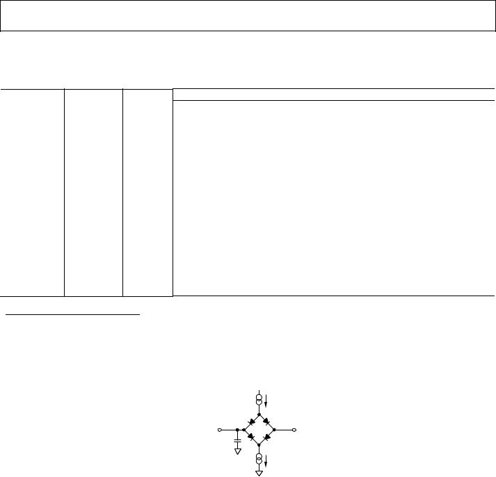
FUNCTIONAL BLOCK DIAGRAM
|
|
AVDD |
|
REFIN/OUT |
AGND |
|
|
|
|
|
|
|
|
|
|
|
|
|
4 |
|
12 |
11 |
|
|
|
|
|
|
|
|
|
|
|
|
|
POWER |
|
X2 |
|
|
|
|
|
|
|
ADE7758 |
|
|
||
|
|
SUPPLY |
|
|
|
|
|
|
|
|
|
|
|
|
|
|
|
|
MONITOR |
|
AVRMSGAIN[11:0] |
|
AVRMSOS[11:0] |
|
|
AVAG[11:0] |
|
|
|
|
|||
|
|
|
|
|
|
|
|
|
|
|
|
|
|
|||
|
|
2.4V |
4kΩ |
|
|
X2 |
|
|
|
|
|
REACTIVE OR |
|
|
||
|
|
|
|
|
|
|
|
|
|
|
|
|
||||
|
|
REF |
|
|
|
|
|
|
|
|
LPF |
|
APPARENT POWER |
|
|
|
|
|
|
|
|
AIGAIN[11:0] |
|
|
|
|
|
|
VARCFNUM[11:0] |
|
|
||
|
|
PGA1 |
|
|
90° PHASE |
AIRMSOS[11:0] |
|
|
|
|
|
|||||
|
|
|
|
|
|
|
|
|
|
|
|
|||||
IAP |
|
|
|
|
SHIFTING FILTER |
|
|
|
|
|
|
|
|
|
||
5 |
+ |
|
ADC |
|
dt |
π |
|
|
|
|
|
DFC |
÷ |
17 |
VARCF |
|
IAN |
6 |
– |
|
|
2 |
|
|
|
|
|
|
|
|
|
||
|
|
HPF |
INTEGRATOR |
|
LPF2 |
|
|
|
|
|
|
|
|
|||
|
|
|
|
|
|
|
|
|
|
VARCFDEN[11:0] |
|
|
||||
|
|
|
PGA2 |
|
|
|
|
|
AVAROS[11:0] |
AVARG[11:0] |
|
|
|
|||
|
|
|
|
|
|
|
|
|
|
|
|
|
||||
VAP 16 |
|
|
|
|
|
|
|
|
|
|
|
|
|
|
||
|
+ |
ADC |
Φ |
|
|
|
|
|
|
|
|
|
|
|
||
|
|
|
– |
|
|
|
|
|
|
|
|
|
|
|
||
|
|
|
|
|
LPF2 |
|
|
|
|
|
|
|
|
|
||
|
|
|
|
|
APHCAL[6:0] |
|
AWG[11:0] |
|
|
|
PHASE B |
|
|
|||
|
|
PGA1 |
|
|
|
AWATTOS[11:0] |
|
|
|
|
AND |
|
|
|||
IBP |
|
|
|
|
|
|
|
|
|
|
|
PHASE C |
|
|
||
7 |
+ |
|
|
|
|
|
|
|
|
|
|
|
|
|||
|
ADC |
|
|
|
|
|
|
|
|
DATA |
|
|
||||
IBN |
8 |
– |
|
ACTIVE/REACTIVE/APPARENT ENERGIES |
|
|
|
|
|
|
|
|
|
|
||
|
|
|
|
|
|
|
|
|
|
|
|
|||||
|
|
|
PGA2 |
|
AND VOLTAGE/CURRENT RMS CALCULATION |
VADIV[7:0] |
|
|
% |
ACTIVE POWER |
|
|
||||
VBP |
|
|
|
FOR PHASE B |
|
|
|
|
|
|||||||
15 |
|
+ |
ADC |
(SEE PHASE A FOR DETAILED SIGNAL PATH) |
|
VARDIV[7:0] |
|
|
% |
APCFNUM[11:0] |
|
|
||||
|
|
PGA1 |
– |
|
|
|
|
|
|
|
|
|
||||
|
|
|
|
|
|
|
|
|
% |
|
DFC |
÷ |
|
|
||
ICP |
|
|
|
|
|
|
WDIV[7:0] |
|
|
1 |
APCF |
|||||
9 |
+ |
|
ADC |
|
|
|
|
|
||||||||
ICN |
10 |
– |
|
ACTIVE/REACTIVE/APPARENT ENERGIES |
|
|
|
|
|
|
|
|
3 |
DVDD |
||
|
|
|
|
|
|
|
|
APCFDEN[11:0] |
||||||||
|
|
|
PGA2 |
|
AND VOLTAGE/CURRENT RMS CALCULATION |
|
|
ADE7758 REGISTERS AND |
2 |
DGND |
||||||
|
|
|
|
FOR PHASE C |
|
|
|
|
|
|||||||
VCP |
14 |
|
+ |
|
|
|
|
SERIAL INTERFACE |
|
|
||||||
|
ADC |
(SEE PHASE A FOR DETAILED SIGNAL PATH) |
|
|
|
|
|
19 |
CLKIN |
|||||||
VN 13 |
|
– |
|
|
|
|
|
|
|
|
|
|
||||
|
|
|
|
|
|
|
|
|
|
|
|
20 |
CLKOUT |
|||
|
|
|
|
|
|
|
|
|
|
|
|
|
|
|
||
|
|
|
|
|
|
|
|
|
22 |
24 |
23 |
21 |
18 |
|
|
-0-001 |
|
|
|
|
|
|
|
|
|
DIN |
DOUT |
SCLK |
CS |
IRQ |
|
|
04443 |
1 Patents Pending.
Figure 1.
Rev. A
Information furnished by Analog Devices is believed to be accurate and reliable. However, no responsibility is assumed by Analog Devices for its use, nor for any infringements of patents or other rights of third parties that may result from its use. Specifications subject to change without notice. No license is granted by implication or otherwise under any patent or patent rights of Analog Devices. Trademarks and registered trademarks are the property of their respective owners.
One Technology Way, P.O. Box 9106, Norwood, MA 02062-9106, U.S.A. Tel: 781.329.4700 www.analog.com Fax: 781.326.8703 © 2004 Analog Devices, Inc. All rights reserved.

ADE7758
TABLE OF CONTENTS |
|
Specifications..................................................................................... |
5 |
Timing Characteristics..................................................................... |
7 |
Absolute Maximum Ratings............................................................ |
9 |
ESD Caution.................................................................................. |
9 |
Pin Configuration and Function Descriptions........................... |
10 |
Terminology .................................................................................... |
12 |
Typical Performance Characteristics ........................................... |
13 |
Theory of Operation ...................................................................... |
19 |
Antialiasing Filter ....................................................................... |
19 |
Analog Inputs.............................................................................. |
19 |
Current Channel ADC............................................................... |
20 |
di/dt Current Sensor and Digital Integrator ........................... |
21 |
Peak Current Detection............................................................. |
22 |
Overcurrent Detection Interrupt ............................................. |
22 |
Voltage Channel ADC ............................................................... |
22 |
Zero-Crossing Detection........................................................... |
24 |
Phase Compensation.................................................................. |
24 |
Period Measurement.................................................................. |
26 |
Line Voltage SAG Detection ..................................................... |
26 |
SAG Level Set.............................................................................. |
26 |
Peak Voltage Detection.............................................................. |
26 |
Phase Sequence Detection......................................................... |
27 |
Power-Supply Monitor............................................................... |
27 |
Reference Circuit ........................................................................ |
28 |
Temperature Measurement ....................................................... |
28 |
Root Mean Square Measurement............................................. |
28 |
Active Power Calculation.......................................................... |
30 |
Reactive Power Calculation ...................................................... |
35 |
Apparent Power Calculation..................................................... |
38 |
Energy Registers Scaling ........................................................... |
41 |
Waveform Sampling Mode ....................................................... |
41 |
Calibration................................................................................... |
41 |
Checksum Register..................................................................... |
54 |
ADE7758 Interrupts................................................................... |
54 |
Using the ADE7758 Interrupts with an MCU........................ |
54 |
Interrupt Timing ........................................................................ |
55 |
ADE7758 Serial Interface.......................................................... |
55 |
ADE7758 Serial Write Operation ............................................ |
56 |
ADE7758 Serial Read Operation ............................................. |
57 |
Accessing the ADE7758 On-Chip Registers........................... |
58 |
Communications Register......................................................... |
58 |
Operational Mode Register (0x13) .......................................... |
61 |
Measurement Mode Register (0x14) ....................................... |
62 |
Waveform Mode Register (0x15) ............................................. |
62 |
Computational Mode Register (0x16)..................................... |
63 |
Line Cycle Accumulation Mode Register (0x17) ................... |
64 |
Interrupt Mask Register (0x18) ................................................ |
65 |
Interrupt Status Register (0x19)/Reset Interrupt Status |
|
Register (0x1A)........................................................................... |
66 |
Outline Dimensions ....................................................................... |
67 |
Ordering Guide .......................................................................... |
67 |
Rev. A | Page 2 of 68

ADE7758
REVISION HISTORY |
|
|
9/04—Changed from Rev. 0 to Rev. A |
|
|
Changed Hexadecimal Notation ...................................... |
Universal |
|
Changes to Features List................................................................... |
|
1 |
Changes to Specifications Table ...................................................... |
|
5 |
Change to Figure 25 ........................................................................ |
|
16 |
Additions to the Analog Inputs Section....................................... |
|
19 |
Added Figures 36 and 37; Renumbered Subsequent Figures .... |
19 |
|
Changes to Period Measurement Section .................................... |
|
26 |
Change to Peak Voltage Detection Section.................................. |
|
26 |
Added Figure 60 .............................................................................. |
|
27 |
Change to the Current RMS Offset Compensation Section...... |
29 |
|
Edits to Active Power Frequency Output Section....................... |
|
33 |
1/04—Revision 0: Initial Version |
|
|
Added Figure 68; Renumbered Subsequent Figures .................. |
33 |
Changes to Reactive Power Frequency Output Section............. |
37 |
Added Figure 73; Renumbered Subsequent Figures .................. |
38 |
Change to Gain Calibration Using Pulse Output Example ....... |
44 |
Changes to Equation 37 ................................................................. |
45 |
Changes to Example—Phase Calibration of Phase A |
|
Using Pulse Output.................................................................. |
45 |
Changes to Equations 56 and 57 ................................................... |
53 |
Addition to the ADE7758 Interrupts Section ............................. |
54 |
Changes to Example-Calibration of RMS Offsets ...................... |
54 |
Addition to Table 20 ....................................................................... |
66 |
Rev. A | Page 3 of 68

ADE7758
GENERAL DESCRIPTION
(Continued from Page 1)
The ADE7758 has a waveform sample register that allows access to the ADC outputs. The part also incorporates a detection circuit for short duration low or high voltage variations. The voltage threshold levels and the duration (number of half-line cycles) of the variation are user programmable. A zero-crossing detection is synchronized with the zero-crossing point of the line voltage of any of the three phases. This information can be used to measure the period of any one of the three voltage inputs. It is also used internally to the chip in the line cycle energy accumulation mode. This mode permits faster and more accurate calibration by synchronizing the energy accumulation with an integer number of line cycles.
Data is read from the ADE7758 via the SPI serial interface. The
interrupt request output (IRQ) is an open-drain, active low
logic output. The IRQ output goes active low when one or more interrupt events have occurred in the ADE7758. A status register indicates the nature of the interrupt. The ADE7758 is available in a 24-lead SOIC package.
Rev. A | Page 4 of 68

ADE7758
SPECIFICATIONS1, 2
AVDD = DVDD = 5 V ± 5%, AGND = DGND = 0 V, on-chip reference, CLKIN = 10 MHz XTAL, TMIN to TMAX = −40°C to +85°C.
Table 1.
Parameter |
Specification |
Unit |
||
|
|
|
|
|
ACCURACY |
|
|
||
Active Energy Measurement Error |
0.1 |
% typ |
||
(per Phase) |
|
|
||
Phase Error between Channels |
|
|
||
(PF = 0.8 Capacitive) |
±0.05 |
°max |
||
(PF = 0.5 Inductive) |
±0.05 |
°max |
||
AC Power Supply Rejection1 |
|
|
||
Output Frequency Variation |
0.01 |
% typ |
||
DC Power Supply Rejection1 |
|
|
||
Output Frequency Variation |
0.01 |
% typ |
||
Active Power Measurement Bandwidth |
14 |
kHz |
||
IRMS Measurement Error |
0.5 |
% typ |
||
IRMS Measurement Bandwidth |
14 |
kHz |
||
VRMS Measurement Error |
0.5 |
% typ |
||
VRMS Measurement Bandwidth |
260 |
Hz |
||
ANALOG INPUTS |
|
|
||
Maximum Signal Levels |
±500 |
mV max |
||
Input Impedance (DC) |
380 |
kΩ min |
||
ADC Offset Error3 |
30 |
mV max |
||
Gain Error1, 3 |
±6 |
% typ |
||
WAVEFORM SAMPLING |
|
|
||
Current Channels |
|
|
||
Signal-to-Noise Plus Distortion |
62 |
dB typ |
||
Bandwidth (−3 dB) |
14 |
kHz |
||
Voltage Channels |
|
|
||
Signal-to-Noise Plus Distortion |
62 |
dB typ |
||
Bandwidth (−3 dB) |
180 |
Hz |
||
REFERENCE INPUT |
|
|
||
REFIN/OUT Input Voltage Range |
2.7 |
V max |
||
|
|
|
2.3 |
V min |
Input Capacitance |
10 |
pF max |
||
|
|
|
|
|
ON-CHIP REFERENCE |
|
|
||
Reference Error |
±200 |
mV max |
||
Current Source |
6 |
µA max |
||
Output Impedance |
4 |
kΩ min |
||
Temperature Coefficient |
30 |
ppm/°C typ |
||
|
|
|
|
|
CLKIN |
|
|
||
Input Clock Frequency |
15 |
MHz max |
||
|
|
|
5 |
MHz min |
|
|
|
|
|
LOGIC INPUTS |
|
|
||
|
|
|
||
DIN, SCLK, CLKIN, and |
CS |
|
|
|
Input High Voltage, VINH |
2.4 |
V min |
||
Input Low Voltage, VINL |
0.8 |
V max |
||
Input Current, IIN |
±3 |
µA max |
||
Input Capacitance, CIN |
10 |
pF max |
||
Test Conditions/Comments
Over a dynamic range of 1000 to 1
Line frequency = 45 Hz to 65 Hz, HPF on Phase lead 37°
Phase lag 60°
AVDD = DVDD = 5 V + 175 mV rms/120 Hz V1P = V2P = V3P = 100 mV rms
AVDD = DVDD = 5 V ± 250 mV dc V1P = V2P = V3P = 100 mV rms
Over a dynamic range of 500:1
Over a dynamic range of 20:1
See the Analog Inputs section
Differential input
Uncalibrated error, see the Terminology section External 2.5 V reference
Sampling CLKIN/128, 10 MHz/128 = 78.1 kSPS See the Current Channel ADC section
See the Voltage Channel ADC section
2.5V + 8%
2.5V – 8%
Nominal 2.4 V at REFIN/OUT pin
All specifications CLKIN of 10 MHz
DVDD = 5 V ± 5%
DVDD = 5 V ± 5%
Typical 10 nA, VIN = 0 V to DVDD
Rev. A | Page 5 of 68

ADE7758
|
Parameter |
Specification |
Unit |
|
Test Conditions/Comments |
||||
|
LOGIC OUTPUTS |
|
|
|
DVDD = 5 V ± 5% |
||||
|
|
|
|
|
|
|
|
is open-drain, 10 kΩ pull-up resistor |
|
|
|
IRQ, |
DOUT, and CLKOUT |
|
|
|
IRQ |
||
|
|
Output High Voltage, VOH |
4 |
V min |
|
ISOURCE = 5 mA |
|||
|
|
Output Low Voltage, VOL |
0.4 |
V max |
|
ISINK = 1 mA |
|||
|
|
APCF and VARCF |
|
|
|
|
|
||
|
|
Output High Voltage, VOH |
4 |
V min |
|
ISOURCE = 8 mA |
|||
|
|
Output Low Voltage, VOL |
1 |
V max |
|
ISINK = 5 mA |
|||
|
|
|
|
|
|
||||
|
POWER SUPPLY |
|
|
For specified performance |
|||||
|
|
AVDD |
4.75 |
V min |
|
5 V − 5% |
|||
|
|
|
|
|
5.25 |
V max |
|
5 V + 5% |
|
|
|
DVDD |
4.75 |
V min |
|
5 V − 5% |
|||
|
|
|
|
|
5.25 |
V max |
|
5 V + 5% |
|
|
|
AIDD |
8 |
mA max |
|
Typically 5 mA |
|||
|
|
DIDD |
13 |
mA max |
|
Typically 9 mA |
|||
|
|
|
|
|
|
|
|
|
|
1 See the Terminology section for a definition of the parameters. 2 See the Typical Performance Characteristics.
3 See the Analog Inputs section.
Rev. A | Page 6 of 68
ADE7758
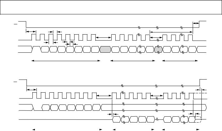
TIMING CHARACTERISTICS1, 2
AVDD = DVDD = 5 V ± 5%, AGND = DGND = 0 V, on-chip reference, CLKIN = 10 MHz XTAL, TMIN to TMAX = −40°C to +85°C.
Table 2.
Parameter |
Specification |
Unit |
|
Test Conditions/Comments |
||||
Write Timing |
|
|
|
|
|
|
|
|
|
|
|
|
|
|
|
||
t1 |
50 |
ns (min) |
|
|
CS |
falling edge to first SCLK falling edge. |
||
t2 |
50 |
ns (min) |
|
|
SCLK logic high pulse width. |
|||
t3 |
50 |
ns (min) |
|
|
SCLK logic low pulse width. |
|||
t4 |
10 |
ns (min) |
|
|
Valid data setup time before falling edge of SCLK. |
|||
t5 |
5 |
ns (min) |
|
|
Data hold time after SCLK falling edge. |
|||
t6 |
900 |
ns (min) |
|
Minimum time between the end of data byte transfers. |
||||
t7 |
50 |
ns (min) |
Minimum time between byte transfers during a serial write. |
|||||
|
|
|
|
|
|
|
||
t8 |
100 |
ns (min) |
|
CS |
hold time after SCLK falling edge. |
|||
Read Timing |
|
|
|
|
|
|
|
|
t9 |
1.1 |
µs (min) |
|
Minimum time between read command (i.e., a write to communication register) and data read. |
||||
t10 |
50 |
ns (min) |
|
Minimum time between data byte transfers during a multibyte read. |
||||
t113 |
30 |
ns (min) |
|
Data access time after SCLK rising edge following a write to the communications register. |
||||
t124 |
100 |
ns (max) |
|
|
Bus relinquish time after falling edge of SCLK. |
|||
|
10 |
ns (min) |
|
|
|
|
|
|
|
|
|
|
|
||||
t134 |
100 |
ns (max) |
|
Bus relinquish time after rising edge of |
CS. |
|
||
10ns (min)
1 Sample tested during initial release and after any redesign or process change that may affect this parameter. All input signals are specified with tr = tf = 5 ns (10% to 90%) and timed from a voltage level of 1.6 V.
2 See the timing diagrams in Figure 3 and Figure 4 and the ADE7758 Serial Interface section.
3 Measured with the load circuit in Figure 2 and defined as the time required for the output to cross 0.8 V or 2.4 V.
4Derived from the measured time taken by the data outputs to change 0.5 V when loaded with the circuit in Figure 2. The measured number is then extrapolated back to remove the effects of charging or discharging the 50 pF capacitor. This means that the time quoted in the timing characteristics is the true bus relinquish time of the part and is independent of the bus loading.
|
200µA |
IOL |
|
TO OUTPUT |
|
2.1V |
|
PIN |
CL |
||
|
|||
|
|
||
|
50pF |
002-0-04443 |
|
|
|
||
|
1.6mA |
IOH |
Figure 2. Load Circuit for Timing Specifications
Rev. A | Page 7 of 68
ADE7758
CS |
t1 |
|
|
|
|
|
|
|
|
|
|
t3 |
|
|
|
|
|
||
|
|
|
|
|
|
|
t7 |
||
SCLK |
|
|
|
|
|
|
|
|
|
|
|
|
|
|
|
|
|
|
|
|
|
|
t2 |
|
t4 |
t5 |
|
|
|
|
|
|
|
|
|
|
|
|
|
DIN |
1 |
A6 |
A5 |
A4 |
A3 |
A2 |
A1 |
A0 |
|
|
|
|
|
COMMAND BYTE |
|
|
|
||
|
|
|
t8 |
|
|
|
t6 |
|
|
t7 |
|
DB7 |
DB0 |
DB7 |
DB0 |
MOST SIGNIFICANT BYTE |
LEAST SIGNIFICANT BYTE |
||
Figure 3. Serial Write Timing
04443-0-003
CS |
|
|
|
|
|
|
|
|
|
|
|
|
t1 |
|
|
|
|
|
|
|
|
|
t13 |
|
|
|
|
|
|
|
|
t9 |
|
t10 |
|
SCLK |
|
|
|
|
|
|
|
|
|
||
|
|
|
|
|
|
|
|
|
|
|
|
DIN |
0 |
A6 |
A5 |
A4 |
A3 |
A2 |
A1 |
A0 |
|
|
|
|
|
|
|
|
|
|
|
t11 |
|
|
t12 |
DOUT |
|
|
|
|
|
|
|
DB7 |
DB0 |
DB7 |
DB0 |
COMMAND BYTE |
|
MOST SIGNIFICANT BYTE |
|
LEAST SIGNIFICANT BYTE |
Figure 4. Serial Read Timing
04443-0-004
Rev. A | Page 8 of 68

ADE7758
ABSOLUTE MAXIMUM RATINGS
TA = 25°C, unless otherwise noted.
Table 3.
AVDD to AGND |
–0.3 V to +7 V |
DVDD to DGND |
–0.3 V to +7 V |
DVDD to AVDD |
–0.3 V to +0.3 V |
Analog Input Voltage to AGND, |
|
IAP, IAN, IBP, IBN, ICP, ICN, VAP, |
–6 V to +6 V |
VBP, VCP, VN |
|
Reference Input Voltage to AGND |
–0.3 V to AVDD + 0.3 V |
Digital Input Voltage to DGND |
–0.3 V to DVDD + 0.3 V |
Digital Output Voltage to DGND |
–0.3 V to DVDD + 0.3 V |
Operating Temperature Range |
|
Industrial |
–40°C to +85°C |
Storage Temperature Range |
–65°C to +150°C |
Junction Temperature |
150°C |
24-Lead SOIC, Power Dissipation |
88 mW |
θJA Thermal Impedance |
53°C/W |
Lead Temperature, Soldering |
|
Vapor Phase (60 sec) |
215°C |
Infrared (15 sec) |
220°C |
Stresses above those listed under Absolute Maximum Ratings may cause permanent damage to the device. This is a stress rating only; functional operation of the device at these or any other conditions above those listed in the operational sections of this specification is not implied. Exposure to absolute maximum rating conditions for extended periods may affect device reliability.
ESD CAUTION
ESD (electrostatic discharge) sensitive device. Electrostatic charges as high as 4000 V readily accumulate on the human body and test equipment and can discharge without detection. Although this product features proprietary ESD protection circuitry, permanent damage may occur on devices subjected to high energy electrostatic discharges. Therefore, proper ESD precautions are recommended to avoid performance degradation or loss of functionality.
Rev. A | Page 9 of 68
ADE7758
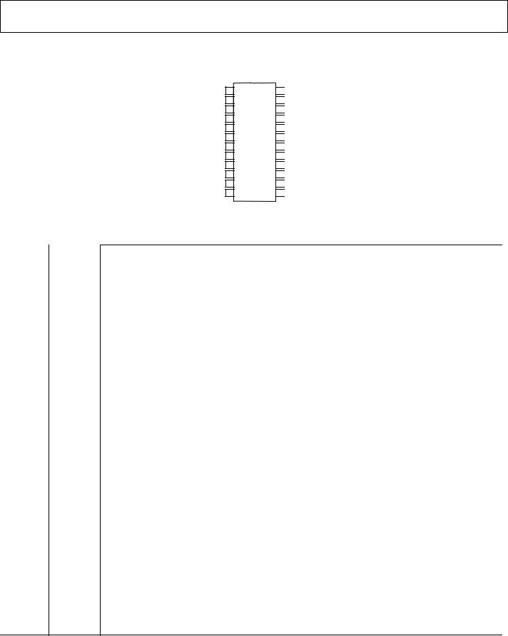
PIN CONFIGURATION AND FUNCTION DESCRIPTIONS
APCF |
1 |
|
|
DGND |
|
|
|
2 |
|
||
DVDD |
|
|
|
3 |
|
||
AVDD |
|
|
|
4 |
|
||
IAP |
|
|
|
5 |
ADE7758 |
||
|
|||
IAN |
6 |
||
TOP VIEW |
|||
IBP |
|
||
7 |
(Not to Scale) |
||
IBN |
|
|
|
8 |
|
||
ICP |
|
|
|
9 |
|
||
ICN |
|
|
|
10 |
|
||
AGND |
|
|
|
11 |
|
||
REFIN/OUT |
|
|
|
12 |
|
24 |
|
DOUT |
|
|||
23 |
|
SCLK |
|
|||
|
|
|||||
22 |
|
DIN |
|
|||
|
|
|||||
21 |
|
|
|
|
|
|
|
CS |
|
||||
20 |
|
CLKOUT |
||||
19 |
|
CLKIN |
|
|||
|
|
|||||
18 |
|
|
|
|
|
|
|
IRQ |
|
||||
17 |
|
VARCF |
||||
16 |
|
VAP |
|
|||
|
|
|||||
15 |
|
VBP |
|
|||
|
|
|||||
14 |
|
VCP |
04443-0-011 |
|||
|
||||||
13 |
|
VN |
||||
|
||||||
|
|
|||||
|
|
Figure 5. Pin Configuration |
Table 4. Pin Function Descriptions |
||
Pin No. |
Mnemonic |
Description |
|
|
|
1 |
APCF |
Active Power Calibration Frequency (APCF) Logic Output. It provides active power information. This output is |
|
|
used for operational and calibration purposes. The full-scale output frequency can be scaled by writing to the |
|
|
APCFNUM and APCFDEN registers (see the Active Power Frequency Output section). |
2 |
DGND |
This provides the ground reference for the digital circuitry in the ADE7758, i.e., the multiplier, filters, and |
|
|
digital-to-frequency converter. Because the digital return currents in the ADE7758 are small, it is acceptable to |
|
|
connect this pin to the analog ground plane of the whole system. However, high bus capacitance on the |
|
|
DOUT pin may result in noisy digital current which could affect performance. |
3 |
DVDD |
Digital Power Supply. This pin provides the supply voltage for the digital circuitry in the ADE7758. The supply |
|
|
voltage should be maintained at 5 V ± 5% for specified operation. This pin should be decoupled to DGND with |
|
|
a 10 µF capacitor in parallel with a ceramic 100 nF capacitor. |
4 |
AVDD |
Analog Power Supply. This pin provides the supply voltage for the analog circuitry in the ADE7758. The supply |
|
|
should be maintained at 5 V ± 5% for specified operation. Every effort should be made to minimize power |
|
|
supply ripple and noise at this pin by the use of proper decoupling. The Typical Performance Characteristics |
|
|
graphs show the power supply rejection performance. This pin should be decoupled to AGND with a 10 µF |
|
|
capacitor in parallel with a ceramic 100 nF capacitor. |
5, 6; |
IAP, IAN; |
Analog Inputs for Current Channel. This channel is used with the current transducer and is referenced in this |
7, 8; |
IBP, IBN; |
document as the current channel. These inputs are fully differential voltage inputs with maximum differential |
9, 10 |
ICP, ICN |
input signal levels of ±0.5 V, ±0.25 V, and ±0.125 V, depending on the gain selections of the internal PGA (see |
|
|
the Analog Inputs sections). |
|
|
All inputs have internal ESD protection circuitry, and in addition, an overvoltage of ±6 V can be sustained on |
|
|
these inputs without risk of permanent damage. |
11 |
AGND |
This pin provides the ground reference for the analog circuitry in the ADE7758, i.e., ADCs, temperature sensor, |
|
|
and reference. This pin should be tied to the analog ground plane or the quietest ground reference in the |
|
|
system. This quiet ground reference should be used for all analog circuitry, for example, antialiasing filters, |
|
|
current, and voltage transducers. In order to keep ground noise around the ADE7758 to a minimum, the quiet |
|
|
ground plane should only be connected to the digital ground plane at one point. It is acceptable to place the |
|
|
entire device on the analog ground plane. |
12REFIN/OUT This pin provides access to the on-chip voltage reference. The on-chip reference has a nominal value of
2.5V ± 8% and a typical temperature coefficient of 30 ppm/°C. An external reference source may also be
connected at this pin. In either case, this pin should be decoupled to AGND with a 1 µF ceramic capacitor.
13, 14, 15, |
VN, VCP, |
Analog Inputs for the Voltage Channel. This channel is used with the voltage transducer and is referenced as |
16 |
VBP, VAP |
the voltage channels in this document. These inputs are single-ended voltage inputs with the maximum |
|
|
signal level of ±0.5 V with respect to VN for specified operation. These inputs are voltage inputs with |
|
|
maximum input signal levels of ±0.5 V, ±0.25 V, and ±0.125 V, depending on the gain selections of the internal |
|
|
PGA (see the Analog Inputs section). |
|
|
All inputs have internal ESD protection circuitry, and in addition, an overvoltage of ±6 V can be sustained on |
|
|
these inputs without risk of permanent damage. |
Rev. A | Page 10 of 68
ADE7758
Pin No. |
Mnemonic |
17VARCF
18IRQ
19CLKIN
20CLKOUT
21CS
22DIN
23SCLK
24DOUT
Description
Reactive Power Calibration Frequency Logic Output. It gives reactive power or apparent power information depending on the setting of the VACF bit of the WAVMODE register. This output is used for operational and calibration purposes. The full-scale output frequency can be scaled by writing to the VARCFNUM and VARCFDEN registers (see the Reactive Power Frequency Output section).
Interrupt Request Output. This is an active low open-drain logic output. Maskable interrupts include: active energy register at half level, apparent energy register at half level, and waveform sampling up to 26 kSPS (see the ADE7758 Interrupts section).
Master Clock for ADCs and Digital Signal Processing. An external clock can be provided at this logic input. Alternatively, a parallel resonant AT crystal can be connected across CLKIN and CLKOUT to provide a clock source for the ADE7758. The clock frequency for specified operation is 10 MHz. Ceramic load capacitors of a few tens of picofarad should be used with the gate oscillator circuit. Refer to the crystal manufacturer’s data sheet for the load capacitance requirements
A crystal can be connected across this pin and CLKIN as previously described to provide a clock source for the ADE7758. The CLKOUT pin can drive one CMOS load when either an external clock is supplied at CLKIN or a crystal is being used.
Chip Select. Part of the 4-wire serial interface. This active low logic input allows the ADE7758 to share the serial bus with several other devices (see the ADE7758 Serial Interface section).
Data Input for the Serial Interface. Data is shifted in at this pin on the falling edge of SCLK (see the ADE7758 Serial Interface section).
Serial Clock Input for the Synchronous Serial Interface. All serial data transfers are synchronized to this clock (see the ADE7758 Serial Interface section). The SCLK has a Schmidt-trigger input for use with a clock source which has a slow edge transition time, for example, opto-isolator outputs.
Data Output for the Serial Interface. Data is shifted out at this pin on the rising edge of SCLK. This logic output is normally in a high impedance state, unless it is driving data onto the serial data bus (see the ADE7758 Serial Interface section).
Rev. A | Page 11 of 68

ADE7758
TERMINOLOGY
Measurement Error
The error associated with the energy measurement made by the ADE7758 is defined by the following formula
Measurement Error =
Energy Registered by ADE7758 –True Energy ×100% True Energy
Phase Error between Channels
The high-pass filter and digital integrator introduce a slight phase mismatch between the current and the voltage channel. The all-digital design ensures that the phase matching between the current channels and voltage channels in all three phases is within ±0.1° over a range of 45 Hz to 65 Hz and ±0.2° over a range of 40 Hz to 1 kHz. This internal phase mismatch can be combined with the external phase error (from current sensor or component tolerance) and calibrated with the phase calibration registers.
Power Supply Rejection
This quantifies the ADE7758 measurement error as a percentage of reading when the power supplies are varied. For the ac PSR measurement, a reading at nominal supplies (5 V) is taken. A second reading is obtained with the same input signal levels when an ac signal (175 mV rms/100 Hz) is introduced onto the supplies. Any error introduced by this ac signal is expressed as a percentage of reading—see the Measurement Error definition.
For the dc PSR measurement, a reading at nominal supplies
(5 V) is taken. A second reading is obtained with the same input signal levels when the power supplies are varied ±5%. Any error introduced is again expressed as a percentage of the reading.
ADC Offset Error
This refers to the dc offset associated with the analog inputs to the ADCs. It means that with the analog inputs connected to AGND the ADCs still see a dc analog input signal. The magnitude of the offset depends on the gain and input range selection (see the Typical Performance Characteristics section). However, when HPFs are switched on, the offset is removed from the current channels and the power calculation is not affected by this offset.
Gain Error
The gain error in the ADCs of the ADE7758 is defined as the difference between the measured ADC output code (minus the offset) and the ideal output code (see the Current Channel ADC and Voltage Channel ADC sections). The difference is expressed as a percentage of the ideal code.
Gain Error Match
The gain error match is defined as the gain error (minus the offset) obtained when switching between a gain of 1, 2, or 4. It is expressed as a percentage of the output ADC code obtained under a gain of 1.
Rev. A | Page 12 of 68

|
|
|
|
|
|
|
|
|
|
|
ADE7758 |
TYPICAL PERFORMANCE CHARACTERISTICS |
|
|
|
|
|
|
|||||
|
0.5 |
|
|
|
|
|
0.20 |
|
|
|
|
|
PF = 1 |
|
|
|
|
|
|
|
|
|
|
|
0.4 |
|
|
|
|
|
0.15 |
|
|
|
|
|
|
|
|
|
|
|
|
|
|
|
|
|
0.3 |
|
|
|
|
|
0.10 |
|
|
|
|
(%) |
0.2 |
|
|
|
|
(%) |
PF = +0.5, –40°C |
|
|
||
|
|
|
|
|
|
|
|||||
|
|
|
|
|
0.05 |
|
|
|
|
||
ERROR |
0.1 |
|
|
|
|
ERROR |
|
PF = –0.5, +25°C |
|
|
|
|
+25°C |
|
|
|
|
|
|
||||
|
|
|
|
|
|
|
|
|
|||
|
0 |
|
|
|
|
0 |
|
|
|
|
|
PERCENT |
|
|
|
|
PERCENT |
PF = +0.5, +85°C |
|
|
|
||
–0.2 |
|
–40°C |
|
|
|
|
|
|
|||
|
–0.1 |
|
|
|
|
|
–0.05 |
|
|
|
|
|
|
|
|
|
|
|
|
|
|
|
|
|
–0.3 |
|
|
|
|
|
–0.10 |
|
PF = +0.5, +25°C |
|
|
|
|
+85°C |
|
|
|
|
|
|
|
|
|
|
–0.4 |
|
|
-0-04443060 |
|
–0.15 |
|
|
|
-0-04443063 |
|
|
|
|
|
|
|
|
|
||||
|
|
|
|
|
|
|
|
|
|
||
|
|
|
|
|
|
|
|
|
|
|
|
|
–0.5 |
0.1 |
1 |
10 |
100 |
|
–0.20 |
0.1 |
1 |
10 |
100 |
|
0.01 |
|
0.01 |
||||||||
|
|
PERCENT FULL-SCALE CURRENT (%) |
|
|
|
PERCENT FULL-SCALE CURRENT (%) |
|
||||
Figure 6. Active Energy Error as a Percentage of Reading (Gain = +1) over Temperature with Internal Reference and Integrator Off
Figure 9. Active Energy Error as a Percentage of Reading (Gain = +1) over Power Factor with External Reference and Integrator Off
|
0.3 |
|
|
|
|
|
0.2 |
|
|
|
|
(%) |
0.1 |
|
|
PF = +0.5, +25°C |
|
ERROR |
|
|
|
||
|
|
|
PF = +1, +25°C |
|
|
0 |
|
|
|
|
|
PERCENT |
|
|
|
|
|
–0.1 |
|
|
|
|
|
|
|
PF = –0.5, +25°C |
|
||
|
|
|
|
||
|
–0.2 |
|
|
PF = +0.5, +85°C |
|
|
|
|
PF = +0.5, –40°C |
04443-0-061 |
|
|
|
|
|
||
|
–0.3 |
|
|
|
|
|
0.1 |
1 |
10 |
100 |
|
|
0.01 |
||||
|
|
PERCENT FULL-SCALE CURRENT (%) |
|
||
Figure 7. Active Energy Error as a Percentage of Reading (Gain = +1) over Power Factor with Internal Reference and Integrator Off
|
0.3 |
|
|
|
|
|
|
PF = 1 |
|
|
|
|
0.2 |
|
|
|
|
(%) |
0.1 |
|
GAIN = +4 |
|
|
ERROR |
|
|
|
|
|
0 |
|
|
|
|
|
PERCENT |
|
|
|
|
|
–0.1 |
|
|
GAIN = +1 |
|
|
|
|
|
|
||
|
|
|
|
|
|
|
|
|
GAIN = +2 |
|
|
|
–0.2 |
|
|
|
04443-0-062 |
|
–0.3 |
|
|
|
|
|
0.1 |
1 |
10 |
100 |
|
|
0.01 |
PERCENT FULL-SCALE CURRENT (%)
|
|
0.6 |
|
|
|
|
|
|
|
|
|
|
|
|
0.5 |
|
|
|
|
|
|
|
|
|
|
|
|
0.4 |
|
|
|
|
|
|
|
|
|
|
(%) 55Hz |
0.3 |
|
PF = 1 |
|
|
|
|
|
|
|
|
|
|
|
|
|
|
|
|
|
|
|
|||
|
|
|
|
|
|
|
|
|
|
|
||
PERCENT ERROR |
WITH RESPECT TO |
0.2 |
|
|
|
|
|
|
|
|
|
|
0.1 |
|
|
|
|
|
|
|
|
|
|
||
0 |
PF = 0.5 |
|
|
|
|
|
|
|
|
|||
|
|
|
|
|
|
|
|
|
|
|||
–0.1 |
|
|
|
|
|
|
|
|
|
|
||
|
|
|
|
|
|
|
|
|
|
|
||
|
|
–0.2 |
|
|
|
|
|
|
|
|
|
|
|
|
–0.3 |
|
|
|
|
|
|
|
|
|
04443-0-065 |
|
|
–0.4 |
|
|
|
|
|
|
|
|
|
|
|
|
47 |
49 |
51 |
53 |
55 |
57 |
59 |
61 |
63 |
65 |
|
|
|
45 |
||||||||||
LINE FREQUENCY (Hz)
Figure 10. Active Energy Error as a Percentage of Reading (Gain = +1) over Frequency with Internal Reference and Integrator Off
|
|
0.10 |
PF = 1 |
|
|
|
|
|
0.08 |
|
|
|
|
|
|
|
|
|
|
|
|
WITH RESPECT TO 5V; 3A |
0.06 |
|
|
|
|
PERCENT ERROR (%) |
0.04 |
|
|
|
|
|
0.02 |
|
VDD = 5.25V |
|
|
||
–0.0 |
VDD = 5V |
|
|
|
||
–0.2 |
|
|
|
|||
|
|
|
|
|||
–0.04 |
|
|
|
|
||
|
|
VDD = 4.75V |
|
|
||
|
|
–0.06 |
|
|
04443-0-066 |
|
|
|
–0.08 |
|
|
|
|
|
|
–0.10 |
|
|
|
|
|
|
0.1 |
1 |
10 |
100 |
|
|
|
0.01 |
||||
|
|
|
PERCENT FULL-SCALE CURRENT (%) |
|
||
Figure 8. Active Energy Error as a Percentage of Reading over Gain with Internal Reference and Integrator Off
Figure 11. Active Energy Error as a Percentage of Reading (Gain = +1) over Power Supply with Internal Reference and Integrator Off
Rev. A | Page 13 of 68

ADE7758
|
0.25 |
PF = 1 |
|
|
|
|
0.20 |
|
|
|
|
|
|
|
|
|
|
|
0.15 |
|
PHASE A |
|
|
(%) |
0.10 |
|
|
|
|
|
|
|
|
||
|
|
|
ALL PHASES |
||
ERROR |
0 |
|
|
||
PERCENT |
0.05 |
|
|
|
|
–0.10 |
|
|
|
|
|
|
–0.05 |
|
|
|
|
|
|
|
PHASE B |
PHASE C |
|
|
–0.15 |
|
|
|
0-04443-067 |
|
–0.20 |
|
|
|
|
|
|
|
|
|
|
|
–0.25 |
0.1 |
1 |
10 |
100 |
|
0.01 |
||||
|
|
PERCENT FULL-SCALE CURRENT (%) |
|
||
|
Figure 12. APCF Error as a Percentage of Reading (Gain = +1) |
||||
|
|
with Internal Reference and Integrator Off |
|
||
|
0.4 |
|
|
|
|
|
0.3 |
|
|
|
|
(%) |
0.2 |
|
|
|
|
0.1 |
|
|
|
|
|
ERROR |
|
|
|
|
|
0 |
|
PF = 0, +25°C |
|
|
|
PERCENT |
–0.1 |
|
PF = 0, –40°C |
|
|
|
|
|
|
||
|
|
|
|
|
|
|
–0.2 |
|
PF = 0, +85°C |
|
|
|
|
|
|
068-0-04443 |
|
|
–0.3 |
|
|
|
|
|
|
|
|
|
|
|
–0.4 |
0.1 |
1 |
10 |
100 |
|
0.01 |
||||
PERCENT FULL-SCALE CURRENT (%)
Figure 13. Reactive Energy Error as a Percentage of Reading (Gain = +1) over Temperature with Internal Reference and Integrator Off
|
0.8 |
|
|
|
|
|
0.6 |
|
|
|
|
(%) |
0.4 |
|
|
|
|
0.2 |
|
|
PF = 0, +25°C |
|
|
ERROR |
PF = –0.866, +25°C |
|
|
||
0 |
|
|
|||
PERCENT |
–0.2 |
PF = +0.866, –40°C |
PF = +0.866, +25°C |
|
|
|
|
|
|
|
|
|
–0.4 |
|
|
|
|
|
|
|
PF = +0.866, +85°C |
|
069-0-04443 |
|
–0.6 |
|
|
|
|
|
|
|
|
|
|
|
–0.8 |
0.1 |
1 |
10 |
100 |
|
0.01 |
||||
PERCENT FULL-SCALE CURRENT (%)
Figure 14. Reactive Energy Error as a Percentage of Reading (Gain = +1) over Power Factor with Internal Reference and Integrator Off
|
0.3 |
|
|
|
|
|
0.2 |
|
|
|
|
(%) |
0.1 |
|
|
|
|
ERROR |
0 |
PF = 0, +85°C |
|
|
|
|
|
|
|
||
PERCENT |
–0.1 |
|
PF = 0, +25°C |
|
|
|
|
|
|
||
|
|
|
|
|
|
|
|
PF = 0, –40°C |
|
|
|
|
–0.2 |
|
|
|
04443-0-070 |
|
–0.3 |
|
|
|
|
|
0.1 |
1 |
10 |
100 |
|
|
0.01 |
||||
PERCENT FULL-SCALE CURRENT (%)
Figure 15. Reactive Energy Error as a Percentage of Reading (Gain = +1) over Temperature with External Reference and Integrator Off
|
0.3 |
|
|
|
|
|
0.2 |
|
|
PF = +0.866, –40°C |
|
|
|
|
PF = –0.866, +25°C |
||
|
|
|
|
||
(%) |
0.1 |
|
|
|
|
ERROR |
0 |
|
|
|
|
PERCENT |
–0.1 |
|
PF = 0, +25°C |
|
|
|
|
|
|||
|
|
|
|
|
|
|
–0.2 |
PF = +0.866, +85°C |
|
PF = +0.866, +25°C |
|
|
|
|
|
04443-0-071 |
|
|
–0.3 |
|
|
|
|
|
0.1 |
1 |
10 |
100 |
|
|
0.01 |
||||
PERCENT FULL-SCALE CURRENT (%)
Figure 16. Reactive Energy Error as a Percentage of Reading (Gain = +1) over Power Factor with External Reference and Integrator Off
|
|
0.8 |
|
|
|
|
|
|
|
|
|
|
|
|
0.6 |
|
|
|
|
|
|
|
|
|
|
(%) 55Hz |
0.4 |
PF = 0 |
|
|
|
|
|
|
|
|
|
|
|
|
|
|
|
|
|
|
|
|
|||
0.2 |
|
|
|
|
|
|
|
|
|
|
||
PERCENT ERROR |
WITH RESPECT TO |
|
|
|
|
|
|
|
|
|
|
|
0 |
|
|
|
|
|
|
|
|
|
|
||
–0.2 |
PF = 0.866 |
|
|
|
|
|
|
|
|
|||
|
|
|
|
|
|
|
|
|
|
|||
–0.4 |
|
|
|
|
|
|
|
|
|
|
||
|
|
|
|
|
|
|
|
|
|
|
|
|
|
|
–0.6 |
|
|
|
|
|
|
|
|
|
04443-0-072 |
|
|
–0.8 |
|
|
|
|
|
|
|
|
|
|
|
|
47 |
49 |
51 |
53 |
55 |
57 |
59 |
61 |
63 |
65 |
|
|
|
45 |
||||||||||
LINE FREQUENCY (Hz)
Figure 17. Reactive Energy Error as a Percentage of Reading (Gain = +1) over Frequency with Internal Reference and Integrator Off
Rev. A | Page 14 of 68
|
0.10 |
|
|
|
|
|
0.08 |
|
|
|
|
ERRORPERCENT(%) TORESPECTWITH5V; 3A |
0.06 |
|
|
5.25V |
|
|
|
|
|
||
0.04 |
|
|
|
|
|
0.02 |
|
|
|
5V |
|
|
|
|
|
||
|
|
|
|
|
|
|
0 |
|
|
|
|
|
–0.02 |
|
|
|
|
|
–0.04 |
|
|
|
|
|
–0.06 |
|
4.75V |
|
|
|
|
|
|
0-04443-073 |
|
|
–0.08 |
|
|
|
|
|
|
|
|
|
|
|
–0.10 |
0.1 |
1 |
10 |
100 |
|
0.01 |
PERCENT FULL-SCALE CURRENT (%)
Figure 18. Reactive Energy Error as a Percentage of Reading (Gain = +1) over Supply with Internal Reference and Integrator Off
|
0.3 |
|
|
|
|
|
|
PF = 0 |
|
|
|
|
0.2 |
GAIN = +2 |
|
|
|
|
|
|
|
|
|
(%) |
0.1 |
GAIN = +4 |
|
|
|
|
|
|
|
||
ERROR |
0 |
|
|
|
|
PERCENT |
|
GAIN = +1 |
|
|
|
|
|
|
|
|
|
|
–0.1 |
|
|
|
|
|
–0.2 |
|
|
|
04443-0-074 |
|
–0.3 |
|
|
|
|
|
0.1 |
1 |
10 |
100 |
|
|
0.01 |
PERCENT FULL-SCALE CURRENT (%)
Figure 19. Reactive Energy Error as a Percentage of Reading over Gain with Internal Reference and Integrator Off
|
0.4 |
|
|
|
|
|
|
PF = 1 |
|
|
|
|
0.3 |
|
|
|
|
(%) |
0.2 |
ALL PHASES |
|
|
|
|
|
|
|||
|
|
PHASE C |
|
|
|
ERROR |
0.1 |
|
|
|
|
|
|
|
|
||
0 |
|
|
|
|
|
PERCENT |
–0.1 |
|
PHASE B |
|
|
|
|
|
|
||
|
|
|
|
|
|
|
–0.2 |
PHASE A |
|
|
|
|
|
|
|
075-0-04443 |
|
|
–0.3 |
|
|
|
|
|
|
|
|
|
|
|
–0.4 |
0.1 |
1 |
10 |
100 |
|
0.01 |
||||
PERCENT FULL-SCALE CURRENT (%)
Figure 20. VARCF Error as a Percentage of Reading (Gain = +1) with Internal Reference and Integrator Off
ADE7758
|
0.3 |
|
|
|
|
|
0.2 |
|
|
|
|
(%) |
0.1 |
|
|
–40°C |
|
ERROR |
0 |
|
|
|
|
PERCENT |
–0.1 |
|
|
+25°C |
|
|
|
|
|
||
|
|
|
|
|
|
|
|
|
|
+85°C |
|
|
–0.2 |
|
|
|
04443-0-076 |
|
–0.3 |
|
|
|
|
|
0.1 |
1 |
10 |
100 |
|
|
0.01 |
PERCENT FULL-SCALE CURRENT (%)
Figure 21. Active Energy Error as a Percentage of Reading (Gain = +4) over Temperature with Internal Reference and Integrator On
|
0.5 |
|
|
|
|
|
0.4 |
|
|
|
|
|
0.3 |
|
|
PF = +0.5, –40°C |
|
|
|
|
|
|
|
(%) |
0.2 |
PF = +0.5, +25°C |
|
|
|
|
|
|
|||
ERROR |
0.1 |
|
|
|
|
0 |
|
|
|
|
|
PERCENT |
–0.1 |
|
PF = +1, +25°C |
PF = –0.5, +25°C |
|
–0.2 |
|
|
|||
|
|
|
|
||
|
–0.3 |
|
PF = +0.5, +85°C |
|
|
|
|
|
|
04443-0-077 |
|
|
–0.4 |
|
|
|
|
|
–0.5 |
|
|
|
|
|
0.1 |
1 |
10 |
100 |
|
|
0.01 |
||||
|
|
PERCENT FULL-SCALE CURRENT (%) |
|
||
Figure 22. Active Energy Error as a Percentage of Reading (Gain = +4) over Power Factor with Internal Reference and Integrator On
|
0.8 |
|
|
|
|
|
0.6 |
|
|
|
|
|
0.4 |
PF = –0.866, –40°C |
|
||
(%) |
|
|
|
|
|
0.2 |
|
|
|
|
|
ERROR |
PF = 0, +25°C |
|
|
|
|
0 |
|
|
|
||
PERCENT |
–0.2 |
PF = +0.866, +25°C |
|
PF = –0.866, +25°C |
|
|
|
|
|||
|
|
|
|
||
|
–0.4 |
|
|
|
|
|
–0.6 |
|
|
PF = –0.866, +85°C |
078-0-04443 |
|
|
|
|
||
|
|
|
|
|
|
|
–0.8 |
0.1 |
1 |
10 |
100 |
|
0.01 |
||||
PERCENT FULL-SCALE CURRENT (%)
Figure 23. Active Energy Error as a Percentage of Reading (Gain = +4) over Power Factor with Internal Reference and Integrator On
Rev. A | Page 15 of 68

ADE7758
|
0.4 |
|
|
|
PF = 0 |
|
0.3 |
|
|
|
|
|
|
|
|
|
|
|
0.2 |
|
|
–40°C |
|
(%) |
0.1 |
|
|
|
|
|
|
|
|
||
ERROR |
0 |
|
|
+25°C |
|
PERCENT |
–0.1 |
|
|
|
|
|
|
|
|
|
|
|
–0.2 |
|
|
|
|
|
–0.3 |
|
|
|
0-04443-079 |
|
–0.4 |
|
|
|
|
|
|
|
|
|
|
|
–0.5 |
|
|
+85°C |
|
|
0.1 |
1 |
10 |
100 |
|
|
0.01 |
PERCENT FULL-SCALE CURRENT (%)
Figure 24. Reactive Energy Error as a Percentage of Reading (Gain = +4) over Temperature with Internal Reference and Integrator On
|
0.5 |
|
|
|
|
|
|
|
|
|
|
|
0.4 |
|
|
|
|
|
|
|
|
|
|
|
0.3 |
|
|
|
|
|
|
|
|
|
|
(%) |
0.2 |
|
|
|
|
|
|
|
|
|
|
|
|
|
|
|
|
|
|
|
|
|
|
ERROR |
0.1 |
|
|
|
|
|
|
|
|
|
|
0 |
|
|
|
|
|
|
|
|
PF = 0.5 |
|
|
PERCENT |
|
|
|
|
|
|
|
|
|
|
|
–0.1 |
|
|
|
|
|
|
|
|
|
|
|
–0.2 |
|
|
|
|
|
|
|
|
PF = 1 |
|
|
|
|
|
|
|
|
|
|
|
|
|
|
|
–0.3 |
|
|
|
|
|
|
|
|
|
|
|
–0.4 |
|
|
|
|
|
|
|
|
|
04443-0-080 |
|
–0.5 |
|
|
|
|
|
|
|
|
|
|
|
47 |
49 |
51 |
53 |
55 |
57 |
59 |
61 |
63 |
65 |
|
|
45 |
LINE FREQUENCY (Hz)
Figure 25. Active Energy Error as a Percentage of Reading (Gain = +4) over Frequency with Internal Reference and Integrator On
|
1.2 |
|
|
|
|
|
|
|
|
|
|
|
1.0 |
|
|
|
|
|
|
|
|
|
|
|
0.8 |
|
|
|
|
|
|
|
|
|
|
(%) |
0.6 |
|
|
|
|
|
|
|
|
|
|
|
|
|
|
|
|
|
|
|
|
|
|
ERROR |
0.4 |
|
|
|
|
|
|
|
PF = 0 |
|
|
|
|
|
|
|
|
|
|
|
|||
0.2 |
|
|
|
|
|
|
|
|
|
|
|
PERCENT |
0 |
|
|
|
|
|
|
|
|
|
|
–0.2 |
|
|
|
|
|
|
|
PF = 0.866 |
|
||
|
|
|
|
|
|
|
|
|
|
||
|
–0.4 |
|
|
|
|
|
|
|
|
|
|
|
–0.6 |
|
|
|
|
|
|
|
|
|
04443-0-081 |
|
–0.8 |
|
|
|
|
|
|
|
|
|
|
|
47 |
49 |
51 |
53 |
55 |
57 |
59 |
61 |
63 |
65 |
|
|
45 |
||||||||||
LINE FREQUENCY (Hz)
Figure 26. Reactive Energy Error as a Percentage of Reading (Gain = +4) over Frequency with Internal Reference and Integrator On
|
0.8 |
|
|
|
|
|
0.6 |
|
|
|
|
|
0.4 |
|
|
|
|
(%) |
0.2 |
|
|
|
|
–0.2 |
|
|
|
|
|
ERROR |
|
|
|
|
|
PERCENT |
0 |
|
|
|
|
–0.6 |
PF = 0.5 |
|
|
|
|
|
–0.4 |
|
|
|
|
|
–0.8 |
PF = 1 |
|
|
|
|
|
|
|
0-04443-082 |
|
|
–1.0 |
|
|
|
|
|
|
|
|
|
|
|
–1.2 |
0.1 |
1 |
10 |
100 |
|
0.01 |
PERCENT FULL-SCALE CURRENT (%)
Figure 27. IRMS Error as a Percentage of Reading (Gain = +1) with Internal Reference and Integrator Off
|
0.8 |
|
|
|
|
0.6 |
|
|
|
|
0.4 |
|
|
|
(%) |
0.2 |
|
PF = –0.5 |
|
ERROR |
|
|
|
|
0 |
|
|
|
|
|
|
PF = +1 |
|
|
PERCENT |
–0.2 |
|
|
|
|
|
|
||
–0.4 |
|
|
|
|
|
|
|
|
|
|
–0.6 |
|
|
|
|
–0.8 |
|
|
04443-0-083 |
|
–1.0 |
|
|
|
|
1 |
10 |
100 |
|
|
0.1 |
|||
|
|
PERCENT FULL-SCALE CURRENT (%) |
|
|
Figure 28. IRMS Error as a Percentage of Reading (Gain = +4) with Internal Reference and Integrator On
|
0.4 |
|
|
|
0.3 |
|
|
(%) |
0.2 |
|
|
0.1 |
|
|
|
ERROR |
|
|
|
0 |
|
|
|
PERCENT |
–0.1 |
|
|
|
|
|
|
|
–0.2 |
|
084-0-04443 |
|
–0.3 |
|
|
|
|
|
|
|
–0.4 |
10 |
100 |
|
1 |
VOLTAGE (V)
Figure 29. VRMS Error as a Percentage of Reading (Gain = +1) with Internal Reference
Rev. A | Page 16 of 68

PERCENT ERROR (%)
|
|
|
|
|
|
|
|
|
|
|
|
|
ADE7758 |
1.5 |
|
|
|
|
|
21 |
|
|
|
|
|
MEAN: 6.5149 |
|
|
|
|
|
|
|
|
|
|
|
|
|||
|
|
|
|
|
|
|
|
|
|
|
|
SD: 2.816 |
|
1.0 |
|
|
|
|
|
18 |
|
|
|
|
|
|
|
|
|
–40°C |
|
|
|
|
|
|
|
|
|
|
|
0.5 |
|
|
|
|
|
15 |
|
|
|
|
|
|
|
|
|
|
|
|
|
|
|
|
|
|
|
|
|
0 |
+25°C |
|
|
|
HITS |
12 |
|
|
|
|
|
|
|
|
|
|
|
|
|
|
|
|
|
|
|
||
|
|
|
|
|
|
9 |
|
|
|
|
|
|
|
–0.5 |
|
|
|
|
|
6 |
|
|
|
|
|
|
|
|
+85°C |
|
|
|
|
|
|
|
|
|
|
|
|
|
|
|
|
|
|
|
|
|
|
|
|
|
|
–1.0 |
|
|
|
04443-0-085 |
|
3 |
|
|
|
|
|
|
04443-0-089 |
–1.5 |
|
|
|
|
0 |
|
|
|
|
|
|
||
|
|
|
|
|
–2 |
0 |
2 |
4 |
6 |
8 |
10 |
12 |
|
0.01 |
0.1 |
1 |
10 |
100 |
|
||||||||
|
|
|
|
CH 1 PhB OFFSET (mV) |
|
|
|||||||
|
PERCENT FULL-SCALE CURRENT (%) |
|
|
|
|
|
|
|
|||||
|
|
|
|
|
|
|
|
|
|
|
|||
Figure 30. Apparent Energy Error as a Percentage of Reading (Gain = +1) over |
Figure 32. Phase B Channel 1 Offset Distribution |
Temperature with Internal Reference and Integrator Off |
|
|
|
|
|
|
|
|
MEAN: 5.55393 |
||
18 |
|
|
|
|
|
|
SD: 3.2985 |
|
|
|
|
|
|
|
|
|
|
||
15 |
|
|
|
|
|
|
|
|
|
12 |
|
|
|
|
|
|
|
|
|
HITS |
|
|
|
|
|
|
|
|
|
9 |
|
|
|
|
|
|
|
|
|
6 |
|
|
|
|
|
|
|
|
|
3 |
|
|
|
|
|
|
|
04443-0-088 |
|
0 |
|
|
|
|
|
|
|
||
–2 |
0 |
2 |
4 |
6 |
8 |
10 |
12 |
||
–4 |
|||||||||
CH 1 PhA OFFSET (mV)
Figure 31. Phase A Channel 1 Offset Distribution
HITS
12 |
|
|
|
|
|
|
|
|
|
|
|
|
|
MEAN: 6.69333 |
|
|
|
|
|
|
|
|
|
|
|
|
|||
|
|
|
|
|
|
|
|
|
|
|
|
|
|
SD: 2.70443 |
10 |
|
|
|
|
|
|
|
|
|
|
|
|
|
|
|
|
|
|
|
|
|
|
|
|
|
|
|
||
|
|
|
|
|
|
|
|
|
|
|
|
|
|
|
8
6
4
2 |
|
|
|
|
|
04443-0-090 |
|
0 |
|
|
|
|
|
||
4 |
6 |
8 |
10 |
12 |
14 |
||
2 |
|||||||
|
|
CH 1 PhC OFFSET (mV) |
|
|
|||
Figure 33. Phase C Channel 1 Offset Distribution
Rev. A | Page 17 of 68

ADE7758
VDD
CURRENT |
10µF |
100nF |
|
|
|
|
|
|
TRANSFORMER |
3 |
17 |
|
PS2501-1 |
||||
I |
|
|
4 |
825Ω |
||||
1kΩ |
|
AVDD DVDD VARCF APCF |
1 |
|
|
|||
|
5 |
IAP |
|
|
|
1 |
4 |
|
|
33nF |
|
|
|
||||
|
|
|
ADE7758 |
|
|
TO FREQ. |
||
RB |
|
|
|
|
COUNTER |
|||
|
1kΩ |
6 |
IAN |
|
|
|
2 |
3 |
|
33nF |
|
|
22pF |
||||
|
|
|
|
|
|
|
||
|
|
|
|
CLKOUT 20 |
|
|
||
|
|
|
IBP |
|
|
|
||
SAME AS |
7 |
|
|
10MHz |
|
|
||
IAP, IAN |
8 |
IBN |
|
CLKIN 19 |
|
|
||
|
|
|
|
22pF |
|
|
||
|
|
|
|
|
|
|
|
|
|
|
|
SAME AS |
9 |
ICP |
|
|
DOUT 24 |
|
|
|
|
IAP, IAN |
10 |
ICN |
|
|
SCLK 23 |
TO SPI BUS ONLY USED |
|
1MΩ |
|
|
|
|
|
|
CS 21 |
|
|
|
|
16 |
VAP |
|
|
FOR CALIBRATION |
||
|
|
|
|
|
|
|
|||
|
|
33nF |
|
|
DIN 22 |
|
|||
220V |
1kΩ |
|
|
|
|
|
|||
|
|
|
|
|
|
IRQ 18 |
|
||
|
|
SAME AS VAP |
15 |
VBP |
|
|
|
||
|
|
|
REFIN/OUT 12 |
|
|||||
|
|
SAME AS VAP |
14 |
VCP |
|
100nF 10µF |
|||
|
|
VN |
AGND |
DGND |
|||||
|
|
|
|
|
|
||||
|
CT TURN RATIO 1800:1 |
|
1kΩ |
13 |
11 |
2 |
|
||
|
|
|
|
|
|
||||
|
CHANNEL 2 GAIN = +1 |
|
|
|
|
|
|||
|
|
|
|
|
|
|
|||
|
CHANNEL 1 GAIN |
RB |
|
33nF |
|
|
|
|
|
|
|
1 |
10Ω |
|
|
|
|
|
04443-0-086 |
|
|
2 |
5Ω |
|
|
|
|
|
|
|
|
8 |
1.25Ω |
|
|
|
|
|
|
|
|
4 |
2.5Ω |
|
|
|
|
|
|
Figure 34. Test Circuit for Integrator Off
|
|
|
|
|
|
VDD |
|
|
|
|
|
|
|
di/dt SENSOR |
10µF |
100nF |
|
|
|
|
|
PS2501-1 |
|||
|
|
|
|
4 |
3 |
17 |
|
|
825Ω |
|||
|
I |
|
|
|
|
|
||||||
|
|
|
|
AVDD DVDD VARCF APCF |
1 |
|
|
|||||
|
1kΩ |
1kΩ |
|
|
|
|
||||||
|
|
5 |
IAP |
|
|
|
|
|
1 |
4 |
||
|
|
33nF |
33nF |
|
|
|
|
|
||||
|
|
|
|
ADE7758 |
|
|
|
|
TO FREQ. |
|||
|
|
1kΩ |
1kΩ |
|
|
|
|
|
|
COUNTER |
||
|
|
6 |
IAN |
|
|
|
|
|
2 |
3 |
||
|
|
33nF |
33nF |
|
|
|
|
22pF |
||||
|
|
|
|
|
|
|
|
|
|
|||
|
|
|
|
|
|
CLKOUT 20 |
|
|
|
|||
|
|
|
|
7 |
IBP |
|
|
10MHz |
|
|
||
|
|
SAME AS |
|
|
|
|
|
|
||||
|
|
IAP, IAN |
8 |
IBN |
|
|
CLKIN 19 |
|
|
|
||
|
|
|
|
|
|
|
|
22pF |
|
|
||
|
|
|
|
|
ICP |
|
|
DOUT 24 |
|
|
||
|
|
SAME AS |
9 |
|
|
|
|
|
||||
|
|
IAP, IAN |
10 |
ICN |
|
|
SCLK 23 |
TO SPI BUS ONLY USED |
||||
|
1MΩ |
|
|
|
|
|
|
CS |
21 |
|||
|
|
|
16 |
VAP |
|
|
FOR CALIBRATION |
|
||||
|
|
|
|
|
|
|
|
|
||||
|
|
33nF |
|
|
|
DIN 22 |
|
|
|
|||
220V |
1kΩ |
|
|
|
|
|
|
|
|
|||
|
|
|
|
|
|
IRQ 18 |
|
|
|
|||
|
|
SAME AS VAP |
15 |
VBP |
|
|
|
|
|
|||
|
|
|
REFIN/OUT 12 |
|
|
|
||||||
|
|
SAME AS VAP |
14 |
VCP |
|
100nF |
10µF |
|
||||
|
|
VN |
AGND |
DGND |
|
|
||||||
|
|
|
|
|
|
|
|
|||||
|
|
|
|
|
1kΩ |
13 |
11 |
2 |
|
|
|
|
|
CHANNEL 1 GAIN = +8 |
|
|
|
|
|
|
|
087-0-04443 |
|||
|
|
|
|
|
|
|
|
|
||||
|
CHANNEL 2 GAIN = +1 |
|
33nF |
|
|
|
|
|
|
|||
|
|
|
|
|
|
|
|
|
|
|
||
Figure 35. Test Circuit for Integrator On
Rev. A | Page 18 of 68

THEORY OF OPERATION
ANTIALIASING FILTER
The need for this filter is that it prevents aliasing. Aliasing is an artifact of all sampled systems. Input signals with frequency components higher than half the ADC sampling rate distort the sampled signal at a frequency below half the sampling rate. This will happen with all ADCs, regardless of the architecture. The combination of the high sampling rate ∑-∆ ADC used in the ADE7758 with the relatively low bandwidth of the energy meter allows a very simple low-pass filter (LPF) to be used as an antialiasing filter. A simple RC filter (single pole) with a corner frequency of 10 kHz produces an attenuation of approximately 40 dB at 833 kHz. This is usually sufficient to eliminate the effects of aliasing.
ANALOG INPUTS
The ADE7758 has a total of six analog inputs divided into two channels: current and voltage. The current channel consists of three pairs of fully differential voltage inputs: IAP and IAN, IBP and IBN, and ICP and ICN. These fully differential voltage input pairs have a maximum differential signal of ±0.5 V. The current channel has a programmable gain amplifier (PGA) with possible gain selection of 1, 2, or 4. In addition to the PGA, the current channels also have a full-scale input range selection for the ADC. The ADC analog input range selection is also made using the gain register (see Figure 38). As mentioned previously, the maximum differential input voltage is ±0.5 V. However, by using Bit 3 and Bit 4 in the gain register, the maximum ADC input voltage can be set to ±0.5 V, ±0.25 V, or ±0.125 V on the current channels. This is achieved by adjusting the ADC reference (see the Reference Circuit section).
Figure 36 shows the maximum signal levels on the current channel inputs. The maximum common-mode signal is ±25 mV as shown in Figure 36.
V1 + V2 |
|
|
|
+500mV |
|
|
|
|
|
IAP, IBP, |
|
DIFFERENTIAL INPUT |
OR ICP |
|
|
V1 |
|
||
V1 + V2 = 500mV MAX PEAK |
|
||
VCM |
|
V2 IAN, IBN, |
|
COMMON-MODE |
V |
0-108 |
|
±25mV MAX |
CM |
OR ICN |
|
–500mV |
|
|
04443- |
Figure 36. Maximum Signal Levels, Current Channels, Gain = 1
The voltage channel has three single-ended voltage inputs: VAP, VBP, and VCP. These single-ended voltage inputs have a maximum input voltage of ±0.5 V with respect to VN. Both the current and voltage channel have a PGA with possible gain selections of 1, 2, or 4. The same gain is applied to all the inputs of each channel.
ADE7758
Figure 37 shows the maximum signal levels on the voltage channel inputs. The maximum common-mode signal is ±25 mV as shown in Figure 36.
V2 |
|
|
+500mV |
|
VAP, VBP, |
|
|
OR VCP |
|
SINGLE-ENDED INPUT |
V2 VN |
VCM |
±500mV MAX PEAK |
|
COMMON-MODE |
|
|
|
VCM |
|
|
±25mV MAX |
|
|
|
04443-0-109 |
–500mV |
AGND |
|
|
|
|
Figure 37. Maximum Signal Levels, Voltage Channels, Gain = 1
The gain selections are made by writing to the gain register. Bit 0 to Bit 1 select the gain for the PGA in the fully differential current channel. The gain selection for the PGA in the singleended voltage channel is made via Bit 5 to Bit 6. Figure 38 shows how a gain selection for the current channel is made using the gain register.
|
GAIN[7:0] |
|
GAIN (K) |
|
SELECTION |
IAP, IBP, ICP |
|
VIN |
K × VIN |
IAN, IBN, ICN |
0-012 |
|
04443- |
Figure 38. PGA in Current Channel
Figure 39 shows how the gain settings in PGA 1 (current channel) and PGA 2 (voltage channel) are selected by various bits in the gain register.
GAIN REGISTER*
CURRENT AND VOLTAGE CHANNEL PGA CONTROL
7 |
6 |
5 |
4 |
3 |
|
2 |
1 |
0 |
|
||
|
0 |
0 |
0 |
0 |
|
0 |
|
0 |
0 |
0 |
ADDRESS: 0x23 |
|
|
|
|
|
|
|
|
|
|
|
|
INTEGRATOR ENABLE |
|
|
|
|
|
|
|
|
PGA 1 GAIN SELECT |
||
0 = DISABLE |
|
|
|
|
RESERVED |
00 = ×1 |
|||||
1 = ENABLE |
|
|
|
|
01 = ×2 |
||||||
PGA 2 GAIN SELECT |
|
|
|
|
|
|
|
|
10 = ×4 |
||
|
|
CURRENT INPUT FULL-SCALE SELECT |
|||||||||
00 = ×1 |
|
|
|
||||||||
01 = ×2 |
|
|
|
00 |
= 0.5V |
|
|
|
|
||
10 = ×4 |
|
|
|
01 |
= 0.25V |
|
|
|
013 |
||
|
|
|
|
10 |
= 0.125V |
|
|
|
-A- |
||
*REGISTER CONTENTS SHOW POWER-ON DEFAULTS |
04443 |
||||||||||
Figure 39. ADE7758 Analog Gain Register
Bit 7 of the gain register is used to enable the digital integrator in the current signal path. Setting this bit will activate the digital integrator (see the di/dt Current Sensor and Digital Integrator section).
Rev. A | Page 19 of 68
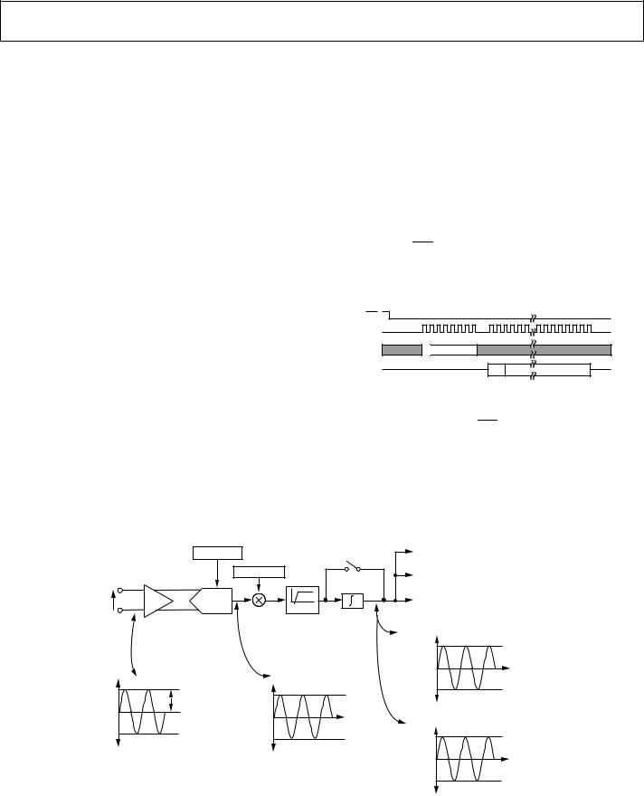
ADE7758
CURRENT CHANNEL ADC
Figure 41 shows the ADC and signal processing path for the input IA of the current channels (same for IB and IC). In waveform sampling mode, the ADC outputs are signed twos complement 24-bit data-words at a maximum of 26.0 kSPS (thousand samples per second). With the specified full-scale analog input signal of ±0.5 V, the ADC produces its maximum output code value (see Figure 41). This diagram shows a fullscale voltage signal being applied to the differential inputs IAP and IAN. The ADC output swings between 0xD7AE14 (−2,642,412) and 0x2851EC (+2,642,412).
Current Waveform Gain Registers
There is a multiplier in the signal path in the current channel for each phase. The current waveform can be changed by ±50% by writing a twos complement number to the 12-bit signed current waveform gain registers (AIGAIN[11:0], BIGAIN[11:0], and CIGAIN[11:0]). For example, if 0x7FF is written to those registers, the ADC output is scaled up by +50%. On the other hand, writing 0x800 scaled by the output –50%. The expression below describes mathematically the function of the current waveform gain registers.
Current Waveform = |
|
|
|||
ADC Output × |
|
+ |
Content of Current Gain Register |
||
1 |
|
|
|||
212 |
|||||
|
|
|
|
||
Changing the content of AIGAIN[11:0], BIGAIN[11:0], or CIGAIN[11:0] affects all calculations based on its current, i.e., it affects the phase’s active/reactive/apparent energy as well as its current rms calculation. In addition, waveform samples are also scaled accordingly.
Current Channel Sampling
The waveform samples of the current channel can be routed to the WFORM register at fixed sampling rates by setting the WAVSEL[2:0] bit in the WAVMODE register to 000 (binary). The phase in which the samples are routed is set by setting the PHSEL[1:0] bits in the WAVMODE register. Energy calculation remains uninterrupted during waveform sampling.
When in waveform sample mode, one of four output sample rates may be chosen by using Bit 5 and Bit 6 of the WAVMODE register (DTRT[1:0]). The output sample rate may be 26.0 kSPS, 13.0 kSPS, 6.5 kSPS, or 3.3 kSPS (see Table 16). By setting the WSMP bit in the interrupt mask register to Logic 1, the interrupt request output IRQ goes active low when a sample is available. The timing is shown in Figure 40. The 24-bit waveform samples are transferred from the ADE7758 one byte (8-bits) at a time, with the most significant byte shifted out first.
IRQ |
|
|
SCLK |
|
|
|
READ FROM WAVEFORM |
|
DIN |
0 12Hex |
|
DOUT |
SGN |
04443-0-015 |
|
CURRENT CHANNEL DATA–24 BITS |
Figure 40. Current Channel Waveform Sampling
The interrupt request output IRQ stays low until the interrupt routine reads the reset status register (see ADE7758 Interrupts).
GAIN[4:3]
2.42V, 1.21V, 0.6V
|
|
REFERENCE |
GAIN[7] |
|
GAIN[1:0] |
AIGAIN[11:0] |
DIGITAL |
IAP |
×1, ×2, ×4 |
|
|
|
INTEGRATOR* |
||
|
|
|
|
VIN |
PGA1 |
ADC |
HPF |
IAN |
|
|
|
|
|
|
CURRENT RMS (IRMS)
CALCULATION
WAVEFORM SAMPLE
REGISTER
ACTIVE AND REACTIVE
POWER CALCULATION
CHANNEL 1 (CURRENT WAVEFORM) 50Hz DATA RANGE AFTER INTEGRATOR
(50Hz AND AIGAIN[11:0] = 0x000)
0x34D1B8
VIN |
CHANNEL 1 |
|
0.5V/GAIN |
(CURRENT WAVEFORM) |
|
0.25V/GAIN |
DATA RANGE |
|
0.125V/GAIN |
0x2851EC |
|
|
||
0V |
0x000000 |
|
|
||
ANALOG |
0xD7AE14 |
|
ADC OUTPUT |
||
INPUT |
||
WORD RANGE |
||
RANGE |
||
|
0x000000
0xCB2E48
60Hz
0x2BE893
0x000000
0xD4176D
CHANNEL 1 (CURRENT WAVEFORM) DATA RANGE AFTER INTEGRATOR (60Hz AND AIGAIN[11:0] = 0x000)
04443-A-014
Figure 41. Current Channel Signal Path
Rev. A | Page 20 of 68
di/dt CURRENT SENSOR AND DIGITAL INTEGRATOR
The di/dt sensor detects changes in the magnetic field caused by the ac current. Figure 42 shows the principle of a di/dt current sensor.
MAGNETIC FIELD CREATED BY CURRENT (DIRECTLY PROPORTIONAL TO CURRENT)
+ EMF (ELECTROMOTIVE FORCE)
– INDUCED BY CHANGES IN 017- 0-04443
MAGNETIC FLUX DENSITY (di/dt)
Figure 42. Principle of a di/dt Current Sensor
The flux density of a magnetic field induced by a current is directly proportional to the magnitude of the current. The changes in the magnetic flux density passing through a conductor loop generate an electromotive force (EMF) between the two ends of the loop. The EMF is a voltage signal that is proportional to the di/dt of the current. The voltage output from the di/dt current sensor is determined by the mutual inductance between the current carrying conductor and the di/dt sensor.
The current signal needs to be recovered from the di/dt signal before it can be used. An integrator is therefore necessary to restore the signal to its original form. The ADE7758 has a builtin digital integrator to recover the current signal from the di/dt sensor. The digital integrator on Channel 1 is switched on by default when the ADE7758 is powered up. Setting the MSB of the GAIN[7:0] register turns on the integrator. Figure 43 to Figure 46 show the magnitude and phase response of the digital integrator.
|
20 |
|
|
|
|
|
|
|
|
|
|
|
|
|
|
|
|
|
|
|
|
|
|
|
|
|
|
|
|
|
|
|
|
|
|
|
|
|
|
|
|
|
|
|
|
|
|
|
|
|
|
|
|
|
|
|
|
|
|
|
|
|
10 |
|
|
|
|
|
|
|
|
|
|
|
|
|
|
|
|
|
|
|
|
|
|
|
|
|
|
|
|
|
|
|
|
|
|
|
|
|
|
|
|
|
|
|
|
|
|
|
|
|
|
|
|
|
|
|
|
|
|
|
|
|
0 |
|
|
|
|
|
|
|
|
|
|
|
|
|
|
|
|
|
|
|
|
|
|
|
|
|
|
|
|
|
|
|
|
|
|
|
|
|
|
|
|
|
|
|
|
|
|
|
|
|
|
|
|
|
|
|
|
|
|
|
|
(dB) |
–10 |
|
|
|
|
|
|
|
|
|
|
|
|
|
|
|
|
|
|
|
|
|
|
|
|
|
|
|
|
|
|
|
|
|
|
|
|
|
|
|
|
|
|
|
|
|
|
|
|
|
|
|
|
|
|
|
|
|
|
||
|
|
|
|
|
|
|
|
|
|
|
|
|
|
|
|
|
|
|
|
|
|
|
|
|
|
|
|
|
|
|
GAIN |
–20 |
|
|
|
|
|
|
|
|
|
|
|
|
|
|
|
|
|
|
|
|
|
|
|
|
|
|
|
|
|
|
|
|
|
|
|
|
|
|
|
|
|
|
|
|
|
|
|
|
|
|
|
|
|
|
|
|
|
|
|
|
|
–30 |
|
|
|
|
|
|
|
|
|
|
|
|
|
|
|
|
|
|
|
|
|
|
|
|
|
|
|
|
|
|
|
|
|
|
|
|
|
|
|
|
|
|
|
|
|
|
|
|
|
|
|
|
|
|
|
|
|
|
|
|
|
–40 |
|
|
|
|
|
|
|
|
|
|
|
|
|
|
|
|
|
|
|
|
|
|
|
|
|
|
|
|
04443-0-091 |
|
|
|
|
|
|
|
|
|
|
|
|
|
|
|
|
|
|
|
|
|
|
|
|
|
|
|
|
|
||
|
–50 |
|
|
|
|
|
|
|
|
|
|
|
|
|
|
|
|
|
|
|
|
|
|
|
|
|
|
|
|
|
|
|
|
|
|
|
|
|
|
|
|
|
|
|
|
|
|
|
|
|
|
|
|
|
|
|
|
|
|
|
|
|
|
|
|
|
|
|
|
|
|
|
|
|
|
|
|
|
|
|
|
|
|
|
|
|
|
|
|
|
|
|
|
10 |
100 |
|
|
|
|
|
|
|
1k |
|
|
|
|
|
|
10k |
|||||||||||||
|
|
|
|
|
|
|
|
|
|
|
|
FREQUENCY (Hz) |
|
|
|
|
|
|
|
|
|
|||||||||
Figure 43. Combined Gain Response of the
Digital Integrator and Phase Compensator
ADE7758
|
80 |
|
|
|
|
|
|
|
|
|
|
|
|
|
|
|
|
|
|
|
|
|
|
|
|
|
|
|
|
|
|
|
|
|
|
|
|
|
|
|
|
|
|
|
|
|
|
|
|
|
|
|
|
|
|
|
|
|
|
|
|
|
81 |
|
|
|
|
|
|
|
|
|
|
|
|
|
|
|
|
|
|
|
|
|
|
|
|
|
|
|
|
|
|
|
|
|
|
|
|
|
|
|
|
|
|
|
|
|
|
|
|
|
|
|
|
|
|
|
|
|
|
|
|
|
82 |
|
|
|
|
|
|
|
|
|
|
|
|
|
|
|
|
|
|
|
|
|
|
|
|
|
|
|
|
|
|
|
|
|
|
|
|
|
|
|
|
|
|
|
|
|
|
|
|
|
|
|
|
|
|
|
|
|
|
|
|
(Degrees) |
83 |
|
|
|
|
|
|
|
|
|
|
|
|
|
|
|
|
|
|
|
|
|
|
|
|
|
|
|
|
|
|
|
|
|
|
|
|
|
|
|
|
|
|
|
|
|
|
|
|
|
|
|
|
|
|
|
|
|
|
||
84 |
|
|
|
|
|
|
|
|
|
|
|
|
|
|
|
|
|
|
|
|
|
|
|
|
|
|
|
|
|
|
|
|
|
|
|
|
|
|
|
|
|
|
|
|
|
|
|
|
|
|
|
|
|
|
|
|
|
|
|
|
|
PHASE |
85 |
|
|
|
|
|
|
|
|
|
|
|
|
|
|
|
|
|
|
|
|
|
|
|
|
|
|
|
|
|
|
|
|
|
|
|
|
|
|
|
|
|
|
|
|
|
|
|
|
|
|
|
|
|
|
|
|
|
|
||
86 |
|
|
|
|
|
|
|
|
|
|
|
|
|
|
|
|
|
|
|
|
|
|
|
|
|
|
|
|
|
|
|
|
|
|
|
|
|
|
|
|
|
|
|
|
|
|
|
|
|
|
|
|
|
|
|
|
|
|
|
||
87 |
|
|
|
|
|
|
|
|
|
|
|
|
|
|
|
|
|
|
|
|
|
|
|
|
|
|
|
|
|
|
|
|
|
|
|
|
|
|
|
|
|
|
|
|
|
|
|
|
|
|
|
|
|
|
|
|
|
|
|
|
|
|
88 |
|
|
|
|
|
|
|
|
|
|
|
|
|
|
|
|
|
|
|
|
|
|
|
|
|
|
|
|
|
|
|
|
|
|
|
|
|
|
|
|
|
|
|
|
|
|
|
|
|
|
|
|
|
|
|
|
|
|
|
|
|
89 |
|
|
|
|
|
|
|
|
|
|
|
|
|
|
|
|
|
|
|
|
|
|
|
|
|
|
|
|
04443-0-092 |
|
|
|
|
|
|
|
|
|
|
|
|
|
|
|
|
|
|
|
|
|
|
|
|
|
|
|
|
|
||
|
90 |
|
|
|
|
|
|
|
|
|
|
|
|
|
|
|
|
|
|
|
|
|
|
|
|
|
|
|
|
|
|
|
|
|
|
|
|
|
|
|
|
|
|
|
|
|
|
|
|
|
|
|
|
|
|
|
|
|
|
||
|
91 |
|
|
|
|
|
|
|
|
|
|
|
|
|
|
|
|
|
|
|
|
|
|
|
|
|
|
|
|
|
|
|
100 |
|
|
|
|
|
|
|
1k |
|
|
|
|
|
|
10k |
|||||||||||||
|
10 |
|
|
|
|
|
|
|
|
|
|
|
|
|
||||||||||||||||
|
|
|
|
|
|
|
|
|
|
|
|
FREQUENCY (Hz) |
|
|
|
|
|
|
|
|
|
|||||||||
Figure 44. Combined Phase Response of the
Digital Integrator and Phase Compensator
|
5 |
|
|
|
|
|
|
|
|
|
|
|
|
|
|
|
|
|
|
|
|
|
|
|
|
|
|
|
|
|
4 |
|
|
|
|
|
|
|
|
|
|
|
|
|
|
|
|
|
|
|
|
|
|
|
|
|
|
|
|
(dB) |
3 |
|
|
|
|
|
|
|
|
|
|
|
|
|
|
|
|
|
|
|
|
|
|
|
|
|
|
||
|
|
|
|
|
|
|
|
|
|
|
|
|
|
|
MAGNITUDE |
2 |
|
|
|
|
|
|
|
|
|
|
|
|
|
|
|
|
|
|
|
|
|
|
|
|
|
|
|
|
|
1 |
|
|
|
|
|
|
|
|
|
|
|
|
|
|
|
|
|
|
|
|
|
|
|
|
|
|
|
|
|
0 |
|
|
|
|
|
|
|
|
|
|
|
|
04443-0-093 |
|
|
|
|
|
|
|
|
|
|
|
|
|
||
|
|
|
|
|
|
|
|
|
|
|
|
|
|
|
|
–1 |
45 |
50 |
55 |
60 |
65 |
70 |
|||||||
|
40 |
|||||||||||||
FREQUENCY (Hz)
Figure 45. Combined Gain Response of the
Digital Integrator and Phase Compensator (40 Hz to 70 Hz)
|
89.80 |
|
|
|
|
|
|
|
|
|
|
|
|
|
|
|
|
|
|
|
|
|
|
|
|
|
|
|
|
|
89.85 |
|
|
|
|
|
|
|
|
|
|
|
|
|
|
|
|
|
|
|
|
|
|
|
|
|
|
|
|
(Degrees) |
89.90 |
|
|
|
|
|
|
|
|
|
|
|
|
|
|
|
|
|
|
|
|
|
|
|
|
|
|
||
89.95 |
|
|
|
|
|
|
|
|
|
|
|
|
|
|
|
|
|
|
|
|
|
|
|
|
|
|
|
||
PHASE |
90.00 |
|
|
|
|
|
|
|
|
|
|
|
|
|
|
|
|
|
|
|
|
|
|
|
|
|
|
||
|
|
|
|
|
|
|
|
|
|
|
|
|
|
|
|
90.05 |
|
|
|
|
|
|
|
|
|
|
|
|
04443-0-094 |
|
|
|
|
|
|
|
|
|
|
|
|
|
||
|
90.10 |
|
|
|
|
|
|
|
|
|
|
|
|
|
|
|
45 |
50 |
55 |
60 |
65 |
70 |
|||||||
|
40 |
|||||||||||||
FREQUENCY (Hz)
Figure 46. Combined Phase Response of the Digital Integrator and Phase Compensator (40 Hz to 70 Hz)
Rev. A | Page 21 of 68
 Loading...