


 Loading...
Analog Devices AD8032BR-REEL7, AD8032BR-REEL, AD8032BR, AD8032BN, AD8032ARM-REEL Datasheet
...
a |
2.7 V, 800 mA, 80 MHz |
Rail-to-Rail I/O Amplifiers |
FEATURES
Low Power
Supply Current 800 mA/Amplifier
Fully Specified at +2.7 V, +5 V and 65 V Supplies
High Speed and Fast Settling on +5 V 80 MHz –3 dB Bandwidth (G = +1) 30 V/ms Slew Rate
125 ns Settling Time to 0.1% Rail-to-Rail Input and Output
No Phase Reversal with Input 0.5 V Beyond Supplies Input CMVR Extends Beyond Rails by 200 mV Output Swing to Within 20 mV of Either Rail
Low Distortion
–62 dB @ 1 MHz, VO = 2 V p-p –86 dB @ 100 kHz, VO = 4.6 V p-p
Output Current: 15 mA High Grade Option
VOS (max) = 1.5 mV
APPLICATIONS
High-Speed Battery-Operated Systems
High Component Density Systems
Portable Test Instruments
A/D Buffer
Active Filters
High-Speed Set-and-Demand Amplifier
GENERAL DESCRIPTION
The AD8031 (single) and AD8032 (dual) single supply voltage feedback amplifiers feature high-speed performance with 80 MHz of small signal bandwidth, 30 V/ s slew rate and 125 ns settling time. This performance is possible while consuming less than 4.0 mW of power from a single +5 V supply. These features increase the operation time of high speed battery-powered systems without compromising dynamic performance.
The products have true single supply capability with rail-to-rail input and output characteristics and are specified for +2.7 V, +5 V and ±5 V supplies. The input voltage range can extend to 500 mV beyond each rail. The output voltage swings to within
20 mV of each rail providing the maximum output dynamic range.
The AD8031/AD8032 also offer excellent signal quality for only 800 A of supply current per amplifier; THD is –62 dBc with a 2 V p-p, 1 MHz output signal and –86 dBc for a 100 kHz, 4.6 V p-p signal on +5 V supply. The low distortion and fast settling time make them ideal as buffers to single supply, A-to-D converters.
Operating on supplies from +2.7 V to +12 V and dual supplies up to
±6 V, the AD8031/AD8032 are ideal for a wide range of applications, from battery-operated systems with large bandwidth requirements
REV. B
Information furnished by Analog Devices is believed to be accurate and reliable. However, no responsibility is assumed by Analog Devices for its use, nor for any infringements of patents or other rights of third parties which may result from its use. No license is granted by implication or otherwise under any patent or patent rights of Analog Devices.
AD8031/AD8032
CONNECTION DIAGRAMS
8-Lead Plastic DIP (N)
and SOIC (R) Packages
NC |
1 |
AD8031 |
8 |
NC |
–IN 2 |
|
7 |
+VS |
|
+IN |
3 |
|
6 |
OUT |
–V |
4 |
|
5 |
NC |
S |
|
|
|
|
NC = NO CONNECT
8-Lead Plastic DIP (N),
SOIC (R) and mSOIC (RM)
Packages
OUT1 |
1 |
8 |
+VS |
–IN1 2 |
7 |
OUT2 |
|
+IN1 |
3 |
6 |
–IN2 |
–V |
4 |
5 |
+IN2 |
S |
AD8032 |
|
|
5-Lead Plastic Surface Mount Package
SOT-23-5 (RT-5) |
|||
VOUT |
1 |
AD8031 |
+VS |
5 |
|||
–V |
2 |
|
|
S |
|
|
|
+IN |
3 |
4 |
–IN |
|
|
(Not to Scale) |
|
to high-speed systems where component density requires lower power dissipation. The AD8031/AD8032 are available in 8-lead plastic DIP and SOIC packages and will operate over the industrial temperature range of –40°C to +85°C. The AD8031A is also available in the space-saving 5-lead SOT-23-5 package and the AD8032A is available in AN 8-lead SOIC package.
1V/Div
2ms/Div
1V/Div
2ms/Div
Input VIN |
Output VOUT |
+5V
 VOUT
VOUT
VIN |
1kV |
1.7pF |
 +2.5V
+2.5V
Circuit Diagram
Figure 1. Rail-to-Rail Performance at 100 kHz
One Technology Way, P.O. Box 9106, Norwood, MA 02062-9106, U.S.A.
Tel: 781/329-4700 |
World Wide Web Site: http://www.analog.com |
Fax: 781/326-8703 |
© Analog Devices, Inc., 1999 |
AD8031/AD8032–SPECIFICATIONS
+2.7 V Supply (@ TA = +258C, VS = +2.7 V, RL = 1 kV to +1.35 V, RF = 2.5 kV unless otherwise noted)
|
|
|
|
|
|
AD8031A/AD8032A |
AD8031B/AD8032B |
|
||||
Parameter |
|
Conditions |
Min |
Typ |
Max |
Min |
Typ |
Max |
Units |
|||
|
|
|
|
|
|
|
|
|
|
|
|
|
DYNAMIC PERFORMANCE |
|
|
|
|
|
|
|
|
|
|
|
|
–3 dB Small Signal Bandwidth |
|
G = +1, VO < 0.4 V p-p |
54 |
80 |
|
54 |
80 |
|
MHz |
|||
Slew Rate |
|
G = –1, VO = 2 V Step |
25 |
30 |
|
25 |
30 |
|
V/µs |
|||
Settling Time to 0.1% |
|
G = –1, VO = 2 V Step, CL = 10 pF |
|
125 |
|
|
125 |
|
ns |
|||
DISTORTION/NOISE PERFORMANCE |
|
|
|
|
|
|
|
|
|
|
||
Total Harmonic Distortion |
|
fC = 1 MHz, VO = 2 V p-p, G = +2 |
|
–62 |
|
|
–62 |
|
dBc |
|||
|
|
|
|
|
||||||||
|
|
fC = 100 kHz, VO = 2 V p-p, G = +2 |
|
–86 |
|
|
–86 |
|
dBc |
|||
Input Voltage Noise |
|
f = 1 kHz |
|
|
15 |
|
|
15 |
|
nV/√Hz |
||
Input Current Noise |
|
f = 100 kHz |
|
2.4 |
|
|
2.4 |
|
pA/√Hz |
|||
|
|
f = 1 kHz |
|
|
5 |
|
|
5 |
|
pA/√Hz |
||
Crosstalk (AD8032 Only) |
|
f = 5 MHz |
|
|
–60 |
|
|
–60 |
|
dB |
||
|
|
|
|
|
|
|
|
|
|
|
|
|
DC PERFORMANCE |
|
|
|
|
|
|
|
|
|
|
|
|
Input Offset Voltage |
|
VCM |
= |
V CC |
; VOUT = 1.35 V |
|
± 1 |
± 6 |
|
± 0.5 |
± 1.5 |
mV |
|
|
|
||||||||||
|
|
|
2 |
|
|
|
|
|
|
|
|
|
|
|
TMIN to TMAX |
|
± 6 |
± 10 |
|
± 1.6 |
± 2.5 |
mV |
|||
Offset Drift |
|
VCM |
= |
V CC |
; VOUT = 1.35 V |
|
10 |
|
|
10 |
|
µV/°C |
|
|
|
|
|
||||||||
|
|
|
2 |
|
|
|
|
|
|
|
|
|
Input Bias Current |
|
VCM |
= |
V CC |
; VOUT = 1.35 V |
|
0.45 |
2 |
|
0.45 |
2 |
µA |
|
|
|
||||||||||
|
|
|
2 |
|
|
|
|
|
|
|
|
|
|
|
TMIN to TMAX |
|
|
2.2 |
|
|
2.2 |
µA |
|||
Input Offset Current |
|
|
|
|
|
|
50 |
500 |
|
50 |
500 |
nA |
|
|
|
V CC |
|
|
|
|
|
|
|
|
|
Open Loop Gain |
|
VCM |
= |
|
; VOUT = 0.35 V to 2.35 V |
76 |
80 |
|
76 |
80 |
|
dB |
|
|
|
||||||||||
|
|
|
2 |
|
|
|
|
|
|
|
|
|
|
|
TMIN to TMAX |
74 |
|
|
74 |
|
|
dB |
|||
INPUT CHARACTERISTICS |
|
|
|
|
|
|
|
|
|
|
|
MΩ |
Common-Mode Input Resistance |
|
|
|
|
|
|
40 |
|
|
40 |
|
|
Differential Input Resistance |
|
|
|
|
|
|
280 |
|
|
280 |
|
kΩ |
Input Capacitance |
|
|
|
|
|
|
1.6 |
|
|
1.6 |
|
pF |
Input Voltage Range |
|
|
|
|
|
|
–0.5 to |
|
|
–0.5 to |
|
|
|
|
|
|
|
|
|
+3.2 |
|
|
+3.2 |
|
V |
Input Common-Mode Voltage Range |
|
|
|
|
|
|
–0.2 to |
|
|
–0.2 to |
|
|
|
|
|
|
|
|
|
+2.9 |
|
|
+2.9 |
|
V |
Common-Mode Rejection Ratio |
|
VCM = 0 V to 2.7 V |
46 |
64 |
|
46 |
64 |
|
dB |
|||
|
|
VCM = 0 V to 1.55 V |
58 |
74 |
|
58 |
74 |
|
dB |
|||
Differential Input Voltage |
|
|
|
|
|
|
|
3.4 |
|
|
3.4 |
V |
|
|
|
|
|
|
|
|
|
|
|
|
|
OUTPUT CHARACTERISTICS |
|
RL = 10 kΩ |
|
|
|
|
|
|
|
|
||
Output Voltage Swing Low |
|
|
+0.05 |
+0.02 |
|
+0.05 |
+0.02 |
|
V |
|||
Output Voltage Swing High |
|
RL = 1 kΩ |
|
+2.6 |
+2.68 |
|
+2.6 |
+2.68 |
|
V |
||
Output Voltage Swing Low |
|
|
+0.15 |
+0.08 |
|
+0.15 |
+0.08 |
|
V |
|||
Output Voltage Swing High |
|
|
|
|
|
+2.55 |
+2.6 |
|
+2.55 |
+2.6 |
|
V |
Output Current |
|
|
|
|
|
|
15 |
|
|
15 |
|
mA |
Short Circuit Current |
|
Sourcing |
|
|
21 |
|
|
21 |
|
mA |
||
|
|
Sinking |
|
|
–34 |
|
|
–34 |
|
mA |
||
Capacitive Load Drive |
|
G = +2 (See Figure 41) |
|
15 |
|
|
15 |
|
pF |
|||
|
|
|
|
|
|
|
|
|
|
|
|
|
POWER SUPPLY |
|
|
|
|
|
|
|
|
|
|
|
|
Operating Range |
|
|
|
|
|
+2.7 |
|
+12 |
+2.7 |
|
+12 |
V |
Quiescent Current per Amplifier |
|
|
|
|
|
|
750 |
1250 |
|
750 |
1250 |
µA |
Power Supply Rejection Ratio |
|
VS– = 0 V to –1 V or |
|
|
|
|
|
|
|
|||
|
|
VS+ = +2.7 V to +3.7 V |
75 |
86 |
|
75 |
86 |
|
dB |
|||
Specifications subject to change without notice.
–2– |
REV. B |
|
SPECIFICATIONS |
|
|
|
|
|
|
|
|
|
|
AD8031/AD8032 |
|||
|
|
|
|
|
|
|
|
|
|
|
|
|
|
|
|
+5 V Supply (@ TA = +258C, VS = +5 V, RL = 1 kV to +2.5 V, RF = 2.5 kV unless otherwise noted) |
|
|
|
|
|
||||||||||
|
|
|
|
|
|
|
|
|
|
|
|
||||
|
|
|
|
|
|
|
AD8031A/AD8032A |
|
AD8031B/AD8032B |
|
|
||||
|
Parameter |
|
Conditions |
Min |
Typ |
Max |
|
Min |
Typ |
Max |
Units |
||||
|
|
|
|
|
|
|
|
|
|
|
|
|
|
|
|
|
DYNAMIC PERFORMANCE |
|
|
|
|
|
|
|
|
|
|
|
|
|
|
|
–3 dB Small Signal Bandwidth |
|
G = +1, VO < 0.4 V p-p |
54 |
80 |
|
|
54 |
80 |
|
MHz |
||||
|
Slew Rate |
|
G = –1, VO = 2 V Step |
27 |
32 |
|
|
27 |
32 |
|
V/µs |
||||
|
Settling Time to 0.1% |
|
G = –1, VO = 2 V Step, CL = 10 pF |
|
125 |
|
|
|
125 |
|
ns |
||||
|
DISTORTION/NOISE PERFORMANCE |
|
|
|
|
|
|
|
|
|
|
|
|
||
|
Total Harmonic Distortion |
|
fC = 1 MHz, VO = 2 V p-p, G = +2 |
|
–62 |
|
|
|
–62 |
|
dBc |
||||
|
|
|
|
|
|
|
|||||||||
|
|
|
fC = 100 kHz, VO = 2 V p-p, G = +2 |
|
–86 |
|
|
|
–86 |
|
dBc |
||||
|
Input Voltage Noise |
|
f = 1 kHz |
|
|
15 |
|
|
|
15 |
|
nV/√Hz |
|||
|
Input Current Noise |
|
f = 100 kHz |
|
2.4 |
|
|
|
2.4 |
|
pA/√Hz |
||||
|
|
|
f = 1 kHz |
|
|
5 |
|
|
|
5 |
|
pA/√Hz |
|||
|
Differential Gain |
|
RL = 1 kΩ |
|
|
0.17 |
|
|
|
0.17 |
|
% |
|
||
|
Differential Phase |
|
RL = 1 kΩ |
|
|
0.11 |
|
|
|
0.11 |
|
Degrees |
|||
|
Crosstalk (AD8032 Only) |
|
f = 5 MHz |
|
|
–60 |
|
|
|
–60 |
|
dB |
|||
|
|
|
|
|
|
|
|
|
|
|
|
|
|
|
|
|
DC PERFORMANCE |
|
|
|
|
|
|
|
|
|
|
|
|
|
|
|
Input Offset Voltage |
|
VCM |
= |
V CC |
; VOUT = 2.5 V |
|
± 1 |
± 6 |
|
|
± 0.5 |
± 1.5 |
mV |
|
|
|
|
|
||||||||||||
|
|
|
|
2 |
|
|
|
|
|
|
|
|
|
|
|
|
|
|
TMIN to TMAX |
|
± 6 |
± 10 |
|
|
± 1.6 |
± 2.5 |
mV |
||||
|
Offset Drift |
|
VCM |
= |
V CC |
; VOUT = 2.5 V |
|
5 |
|
|
|
5 |
|
µV/°C |
|
|
|
|
|
|
|
|
|||||||||
|
|
|
|
2 |
|
|
|
|
|
|
|
|
|
|
|
|
Input Bias Current |
|
VCM |
= |
V CC |
; VOUT = 2.5 V |
|
0.45 |
1.2 |
|
|
0.45 |
1.2 |
µA |
|
|
|
|
|
||||||||||||
|
|
|
|
2 |
|
|
|
|
|
|
|
|
|
|
|
|
|
|
TMIN to TMAX |
|
|
2.0 |
|
|
|
2.0 |
µA |
||||
|
Input Offset Current |
|
|
|
|
|
|
50 |
350 |
|
|
50 |
250 |
nA |
|
|
|
|
|
V CC |
|
|
|
|
|
|
|
|
|
|
|
|
Open Loop Gain |
|
VCM |
= |
|
; VOUT = 1.5 V to 3.5 V |
76 |
82 |
|
|
76 |
82 |
|
dB |
|
|
|
|
|
|
|||||||||||
|
|
|
|
2 |
|
|
|
|
|
|
|
|
|
|
|
|
|
|
TMIN to TMAX |
74 |
|
|
|
74 |
|
|
dB |
|
|||
|
INPUT CHARACTERISTICS |
|
|
|
|
|
|
|
|
|
|
|
|
MΩ |
|
|
Common-Mode Input Resistance |
|
|
|
|
|
|
40 |
|
|
|
40 |
|
||
|
Differential Input Resistance |
|
|
|
|
|
|
280 |
|
|
|
280 |
|
kΩ |
|
|
Input Capacitance |
|
|
|
|
|
|
1.6 |
|
|
|
1.6 |
|
pF |
|
|
Input Voltage Range |
|
|
|
|
|
|
–0.5 to |
|
|
|
–0.5 to |
|
|
|
|
|
|
|
|
|
|
|
+5.5 |
|
|
|
+5.5 |
|
V |
|
|
Input Common-Mode Voltage Range |
|
|
|
|
|
|
–0.2 to |
|
|
|
–0.2 to |
|
|
|
|
|
|
|
|
|
|
|
+5.2 |
|
|
|
+5.2 |
|
V |
|
|
Common-Mode Rejection Ratio |
|
VCM = 0 V to 5 V |
56 |
70 |
|
|
56 |
70 |
|
dB |
||||
|
|
|
VCM = 0 V to 3.8 V |
66 |
80 |
|
|
66 |
80 |
|
dB |
||||
|
Differential Input Voltage |
|
|
|
|
|
|
|
3.4 |
|
|
|
3.4 |
V |
|
|
|
|
|
|
|
|
|
|
|
|
|
|
|
|
|
|
OUTPUT CHARACTERISTICS |
|
RL = 10 kΩ |
|
|
|
|
|
|
|
|
|
|
||
|
Output Voltage Swing Low |
|
|
+0.05 |
+0.02 |
|
|
+0.05 |
+0.02 |
|
V |
||||
|
Output Voltage Swing High |
|
RL = 1 kΩ |
|
+4.95 |
+4.98 |
|
|
+4.95 |
+4.98 |
|
V |
|||
|
Output Voltage Swing Low |
|
|
+0.2 |
+0.1 |
|
|
+0.2 |
+0.1 |
|
V |
||||
|
Output Voltage Swing High |
|
|
|
|
|
+4.8 |
+4.9 |
|
|
+4.8 |
+4.9 |
|
V |
|
|
Output Current |
|
|
|
|
|
|
15 |
|
|
|
15 |
|
mA |
|
|
Short Circuit Current |
|
Sourcing |
|
|
28 |
|
|
|
28 |
|
mA |
|||
|
|
|
Sinking |
|
|
–46 |
|
|
|
–46 |
|
mA |
|||
|
Capacitive Load Drive |
|
G = +2 (See Figure 41) |
|
15 |
|
|
|
15 |
|
pF |
||||
|
|
|
|
|
|
|
|
|
|
|
|
|
|
|
|
|
POWER SUPPLY |
|
|
|
|
|
|
|
|
|
|
|
|
|
|
|
Operating Range |
|
|
|
|
|
+2.7 |
|
+12 |
|
+2.7 |
|
+12 |
V |
|
|
Quiescent Current per Amplifier |
|
|
|
|
|
|
800 |
1400 |
|
|
800 |
1400 |
µA |
|
|
Power Supply Rejection Ratio |
|
VS– = 0 V to –1 V or |
|
|
|
|
|
|
|
|
|
|||
|
|
|
VS+ = +5 V to +6 V |
75 |
86 |
|
|
75 |
86 |
|
dB |
|
|||
Specifications subject to change without notice.
REV. B |
–3– |
AD8031/AD8032–SPECIFICATIONS
65 V Supply (@ TA = +258C, VS = 65 V, RL = 1 kV to 0 V, RF = 2.5 kV unless otherwise noted)
|
|
|
AD8031A/AD8032A |
AD8031B/AD8032B |
|
||||
Parameter |
|
Conditions |
Min |
Typ |
Max |
Min |
Typ |
Max |
Units |
|
|
|
|
|
|
|
|
|
|
DYNAMIC PERFORMANCE |
|
|
|
|
|
|
|
|
|
–3 dB Small Signal Bandwidth |
|
G = +1, VO < 0.4 V p-p |
54 |
80 |
|
54 |
80 |
|
MHz |
Slew Rate |
|
G = –1, VO = 2 V Step |
30 |
35 |
|
30 |
35 |
|
V/µs |
Settling Time to 0.1% |
|
G = –1, VO = 2 V Step, CL = 10 pF |
|
125 |
|
|
125 |
|
ns |
DISTORTION/NOISE PERFORMANCE |
|
|
|
|
|
|
|
||
Total Harmonic Distortion |
|
fC = 1 MHz, VO = 2 V p-p, G = +2 |
|
–62 |
|
|
–62 |
|
dBc |
|
|
|
|
|
|||||
|
|
fC = 100 kHz, VO = 2 V p-p, G = +2 |
|
–86 |
|
|
–86 |
|
dBc |
Input Voltage Noise |
|
f = 1 kHz |
|
15 |
|
|
15 |
|
nV/√Hz |
Input Current Noise |
|
f = 100 kHz |
|
2.4 |
|
|
2.4 |
|
pA/√Hz |
|
|
f = 1 kHz |
|
5 |
|
|
5 |
|
pA/√Hz |
Differential Gain |
|
RL = 1 kΩ |
|
0.15 |
|
|
0.15 |
|
% |
Differential Phase |
|
RL = 1 kΩ |
|
0.15 |
|
|
0.15 |
|
Degrees |
Crosstalk (AD8032 Only) |
|
f = 5 MHz |
|
–60 |
|
|
–60 |
|
dB |
|
|
|
|
|
|
|
|
|
|
DC PERFORMANCE |
|
|
|
± 1 |
± 6 |
|
± 0.5 |
± 1.5 |
|
Input Offset Voltage |
|
VCM = 0 V; VOUT = 0 V |
|
|
mV |
||||
|
|
TMIN to TMAX |
|
± 6 |
± 10 |
|
± 1.6 |
± 2.5 |
mV |
Offset Drift |
|
VCM = 0 V; VOUT = 0 V |
|
5 |
|
|
5 |
|
µV/°C |
Input Bias Current |
|
VCM = 0 V; VOUT = 0 V |
|
0.45 |
1.2 |
|
0.45 |
1.2 |
µA |
|
|
TMIN to TMAX |
|
|
2.0 |
|
|
2.0 |
µA |
Input Offset Current |
|
VCM = 0 V; VOUT = ± 2 V |
|
50 |
350 |
|
50 |
250 |
nA |
Open Loop Gain |
|
76 |
80 |
|
76 |
80 |
|
dB |
|
|
|
TMIN to TMAX |
74 |
|
|
74 |
|
|
dB |
INPUT CHARACTERISTICS |
|
|
|
|
|
|
|
|
MΩ |
Common-Mode Input Resistance |
|
|
|
40 |
|
|
40 |
|
|
Differential Input Resistance |
|
|
|
280 |
|
|
280 |
|
kΩ |
Input Capacitance |
|
|
|
1.6 |
|
|
1.6 |
|
pF |
Input Voltage Range |
|
|
|
–5.5 to |
|
|
–5.5 to |
|
|
|
|
|
|
+5.5 |
|
|
+5.5 |
|
V |
Input Common-Mode Voltage Range |
|
|
|
–5.2 to |
|
|
–5.2 to |
|
|
|
|
|
|
+5.2 |
|
|
+5.2 |
|
V |
Common-Mode Rejection Ratio |
|
VCM = –5 V to +5 V |
60 |
80 |
|
60 |
80 |
|
dB |
|
|
VCM = –5 V to +3.5 V |
66 |
90 |
|
66 |
90 |
|
dB |
Differential/Input Voltage |
|
|
|
|
3.4 |
|
|
3.4 |
V |
|
|
|
|
|
|
|
|
|
|
OUTPUT CHARACTERISTICS |
|
RL = 10 kΩ |
|
|
|
|
|
|
|
Output Voltage Swing Low |
|
–4.94 |
–4.98 |
|
–4.94 |
–4.98 |
|
V |
|
Output Voltage Swing High |
|
RL = 1 kΩ |
+4.94 |
+4.98 |
|
+4.94 |
+4.98 |
|
V |
Output Voltage Swing Low |
|
–4.7 |
–4.85 |
|
–4.7 |
–4.85 |
|
V |
|
Output Voltage Swing High |
|
|
+4.7 |
+4.75 |
|
+4.7 |
+4.75 |
|
V |
Output Current |
|
|
|
15 |
|
|
15 |
|
mA |
Short Circuit Current |
|
Sourcing |
|
35 |
|
|
35 |
|
mA |
|
|
Sinking |
|
–50 |
|
|
–50 |
|
mA |
Capacitive Load Drive |
|
G = +2 (See Figure 41) |
|
15 |
|
|
15 |
|
pF |
|
|
|
|
|
|
|
|
|
|
POWER SUPPLY |
|
|
± 1.35 |
|
± 6 |
± 1.35 |
|
± 6 |
|
Operating Range |
|
|
|
|
V |
||||
Quiescent Current per Amplifier |
|
|
|
900 |
1600 |
|
900 |
1600 |
µA |
Power Supply Rejection Ratio |
|
VS– = –5 V to –6 V or |
|
|
|
|
|
|
|
|
|
VS+ = +5 V to +6 V |
76 |
86 |
|
76 |
86 |
|
dB |
Specifications subject to change without notice.
–4– |
REV. B |
AD8031/AD8032
ABSOLUTE MAXIMUM RATINGS1
Supply Voltage . . . . . . . . . . . . . . . . . . . . . . . . . . . . . . . +12.6 V Internal Power Dissipation2
Plastic DIP Package (N) . . . . . . . . . . . . . . . . . . . 1.3 Watts Small Outline Package (R) . . . . . . . . . . . . . . . . . . 0.8 WattsSOIC (RM) . . . . . . . . . . . . . . . . . . . . . . . . . . . . 0.6 Watts SOT-23-5 (RT) . . . . . . . . . . . . . . . . . . . . . . . . . . 0.5 Watts Input Voltage (Common-Mode) . . . . . . . . . . . . . ±VS ± 0.5 V Differential Input Voltage . . . . . . . . . . . . . . . . . . . . . . . ±3.4 V
Output Short Circuit Duration
. . . . . . . . . . . . . . . . . . . . . . Observe Power Derating Curves Storage Temperature Range (N, R, RM, RT)
. . . . . . . . . . . . . . . . . . . . . . . . . . . . . . . . . . –65°C to +125°C Lead Temperature Range (Soldering 10 sec) . . . . . . . . +300°C
NOTES
1Stresses above those listed under Absolute Maximum Ratings may cause permanent damage to the device. This is a stress rating only; functional operation of the device at these or any other conditions above those indicated in the operational section of this specification is not implied. Exposure to absolute maximum rating conditions for extended periods may affect device reliability.
2Specification is for the device in free air: 8-Lead Plastic DIP Package: θJA = 90°C/W. 8-Lead SOIC Package: θJA = 155°C/W. 8-Lead µSOIC Package: θJA = 200°C/W. 5-Lead SOT-23-5 Package: θJA = 240°C/W.
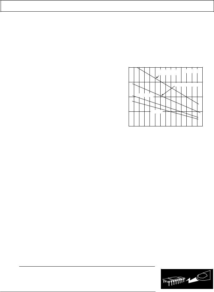
MAXIMUM POWER DISSIPATION
The maximum power that can be safely dissipated by the AD8031/AD8032 are limited by the associated rise in junction temperature. The maximum safe junction temperature for plastic encapsulated devices is determined by the glass transition
temperature of the plastic, approximately +150°C. Exceeding this limit temporarily may cause a shift in parametric performance due to a change in the stresses exerted on the die by the package. Exceeding a junction temperature of +175°C for an extended period can result in device failure.
While the AD8031/AD8032 are internally short circuit protected, this may not be sufficient to guarantee that the maximum junction temperature (+150°C) is not exceeded under all conditions. To ensure proper operation, it is necessary to observe the maximum power derating curves shown in Figure 2.
|
2.0 |
|
|
|
|
|
|
|
|
|
– Watts |
|
|
8-LEAD PLASTIC |
|
TJ = +1508C |
|||||
|
|
DIP PACKAGE |
|
|
|
|
|
|||
1.5 |
|
|
|
|
|
|
|
|
|
|
DISSIPATION |
|
|
|
8-LEAD SOIC PACKAGE |
||||||
|
|
|
|
|||||||
1.0 |
8-LEAD mSOIC |
|
|
|
|
|
|
|
|
|
|
|
|
|
|
|
|
|
|
||
POWER |
|
|
|
|
|
|
|
|
|
|
MAXIMUM |
0.5 |
SOT-23-5 |
|
|
|
|
|
|
|
|
|
|
|
|
|
|
|
|
|
|
|
|
0 |
|
|
|
|
|
|
|
|
|
|
–50 –40–30 –20 –100 |
10 |
20 |
30 |
40 |
50 |
60 |
70 |
80 90 |
|
|
|
AMBIENT TEMPERATURE –8C |
|
|
|
|||||
Figure 2. Maximum Power Dissipation vs. Temperature
ORDERING GUIDE
|
Temperature |
Package |
Package |
Brand |
Model |
Range |
Descriptions |
Options |
Code |
|
|
|
|
|
AD8031AN |
–40°C to +85°C |
8-Lead Plastic DIP |
N-8 |
|
AD8031AR |
–40°C to +85°C |
8-Lead SOIC |
SO-8 |
|
AD8031AR-REEL |
–40°C to +85°C |
13" Tape and Reel |
SO-8 |
|
AD8031AR-REEL7 |
–40°C to +85°C |
7" Tape and Reel |
SO-8 |
|
AD8031ART-REEL |
–40°C to +85°C |
13" Tape and Reel |
RT-5 |
H0A |
AD8031ART-REEL7 |
–40°C to +85°C |
7" Tape and Reel |
RT-5 |
H0A |
AD8031BN |
–40°C to +85°C |
8-Lead Plastic DIP |
N-8 |
|
AD8031BR |
–40°C to +85°C |
8-Lead SOIC |
SO-8 |
|
AD8031BR-REEL |
–40°C to +85°C |
13" Tape and Reel |
SO-8 |
|
AD8031BR-REEL7 |
–40°C to +85°C |
7" Tape and Reel |
SO-8 |
|
AD8032AN |
–40°C to +85°C |
8-Lead Plastic DIP |
N-8 |
|
AD8032AR |
–40°C to +85°C |
8-Lead SOIC |
SO-8 |
|
AD8032AR-REEL |
–40°C to +85°C |
13" Tape and Reel |
SO-8 |
|
AD8032AR-REEL7 |
–40°C to +85°C |
7" Tape and Reel |
SO-8 |
|
AD8032ARM |
–40°C to +85°C |
8-Lead SOIC |
RM-8 |
H9A |
AD8032ARM-REEL |
–40°C to +85°C |
13" Tape and Reel |
RM-8 |
H9A |
AD8032ARM-REEL7 |
–40°C to +85°C |
7" Tape and Reel |
RM-8 |
H9A |
AD8032BN |
–40°C to +85°C |
8-Lead Plastic DIP |
N-8 |
|
AD8032BR |
–40°C to +85°C |
8-Lead SOIC |
SO-8 |
|
AD8032BR-REEL |
–40°C to +85°C |
13" Tape and Reel |
SO-8 |
|
AD8032BR-REEL7 |
–40°C to +85°C |
7" Tape and Reel |
SO-8 |
|
|
|
|
|
|
CAUTION
ESD (electrostatic discharge) sensitive device. Electrostatic charges as high as 4000 V readily accumulate on the human body and test equipment and can discharge without detection. Although the AD8031/AD8032 feature proprietary ESD protection circuitry, permanent damage may occur on devices subjected to high energy electrostatic discharges. Therefore, proper ESD precautions are recommended to avoid performance degradation or loss of functionality.
WARNING! |
ESD SENSITIVE DEVICE |
REV. B |
–5– |
Loading...