


 Loading...
Analog Devices AD7575KN, AD7575JR, AD7575JP, AD7575JN, AD7575BQ Datasheet
...a |
LC2MOS |
|
5 ms 8-Bit ADC with Track/Hold |
||
|
|
|
|
|
AD7575 |
|
|
|
FEATURES
Fast Conversion Time: 5 ms
On-Chip Track/Hold
Low Total Unadjusted Error: 1 LSB Full Power Signal Bandwidth: 50 kHz Single +5 V Supply
100 ns Data Access Time Low Power (15 mW typ) Low Cost
Standard 18-Lead DlPs or 20-Terminal Surface Mount Packages
GENERAL DESCRIPTION
The AD7575 is a high speed 8-bit ADC with a built-in track/ hold function. The successive approximation conversion technique is used to achieve a fast conversion time of 5 s, while the built-in track/hold allows full-scale signals up to 50 kHz (386 mV/ s slew rate) to be digitized. The AD7575 requires only a single +5 V supply and a low cost, 1.23 V bandgap reference in order to convert an input signal range of 0 to 2 VREF.
The AD7575 is designed for easy interfacing to all popular 8-bit microprocessors using standard microprocessor control signals (CS and RD) to control starting of the conversion and reading of the data. The interface logic allows the AD7575 to be easily configured as a memory mapped device, and the part can be interfaced as SLOW-MEMORY or ROM. All data outputs of the AD7575 are latched and three-state buffered to allow direct connection to a microprocessor data bus or I/O port.
The AD7575 is fabricated in an advanced, all ion-implanted high speed Linear Compatible CMOS (LC2MOS) process and is available in a small, 0.3" wide, 18-lead DIP, 18-lead SOIC or in other 20-terminal surface mount packages.
REV. B
Information furnished by Analog Devices is believed to be accurate and reliable. However, no responsibility is assumed by Analog Devices for its use, nor for any infringements of patents or other rights of third parties which may result from its use. No license is granted by implication or otherwise under any patent or patent rights of Analog Devices.
FUNCTIONAL BLOCK DIAGRAM
VDD
AIN |
TRACK |
AD7575 |
|
AND |
|
||
|
HOLD |
COMP |
|
AGND |
|
|
|
VREF |
|
DAC |
|
CLK |
CLOCK |
SAR |
|
OSCILLATOR |
|||
|
|
||
CS |
|
DB7 |
|
CONTROL |
LATCH AND |
||
|
|||
RD |
THREE STATE |
||
LOGIC |
|||
TP |
OUTPUT DRIVERS |
||
|
|||
|
DB0 |
||
|
|
||
|
BUSY |
DGND |
PRODUCT HIGHLIGHTS
1.Fast Conversion Time/Low Power
The fast, 5 s, conversion time of the AD7575 makes it suitable for digitizing wideband signals at audio and ultrasonic frequencies while retaining the advantage of low CMOS power consumption.
2.On-Chip Track/Hold
The on-chip track/hold function is completely self-contained
and requires no external hold capacitor. Signals with slew rates up to 386 mV/ s (e.g., 2.46 V peak-to-peak 50 kHz sine waves) can be digitized with full accuracy.
3.Low Total Unadjusted Error
The zero, full-scale and linearity errors of the AD7575 are so low that the total unadjusted error at any point on the transfer function is less than 1 LSB, and offset and gain adjustments are not required.
4.Single Supply Operation
Operation from a single +5 V supply with a low cost +1.23 V bandgap reference allows the AD7575 to be used in 5 V microprocessor systems without any additional power supplies.
5.Fast Digital Interface
Fast interface timing allows the AD7575 to interface easily to the fast versions of most popular microprocessors such as the Z80H, 8085A-2, 6502B, 68B09 and the DSP processor, the TMS32010.
One Technology Way, P.O. Box 9106, Norwood, MA 02062-9106, U.S.A.
Tel: 781/329-4700 |
World Wide Web Site: http://www.analog.com |
Fax: 781/326-8703 |
© Analog Devices, Inc., 1998 |

|
|
|
|
|
|
|
(VDD = +5 V, VREF = +1.23 V, AGND = DGND = 0 V; fCLK = 4 MHz external; |
||||
AD7575–SPECIFICATIONS all specifications TMIN to TMAX unless otherwise noted) |
|||||||||||
Parameter |
J, A Versions1 |
K, B Versions |
S Version |
T Version |
Units |
Conditions/Comments |
|||||
ACCURACY |
|
|
|
|
|
|
|||||
|
Resolution |
8 |
8 |
8 |
8 |
Bits |
|
||||
|
Total Unadjusted Error |
±2 |
±1 |
±2 |
±1 |
LSB max |
|
||||
|
Relative Accuracy |
±1 |
±1/2 |
±1 |
±1/2 |
LSB max |
|
||||
|
Minimum Resolution for Which |
|
|
|
|
|
|
||||
|
No Missing Codes Is Guaranteed |
8 |
8 |
8 |
8 |
Bits max |
|
||||
|
Full-Scale Error |
|
|
|
|
|
|
||||
|
+25°C |
±1 |
±1 |
±1 |
±1 |
LSB max |
Full-Scale TC Is Typically 5 ppm/°C |
||||
|
TMIN to TMAX |
±1 |
±1 |
±1 |
±1 |
LSB max |
|
||||
|
Offset Error2 |
|
|
|
|
|
|
||||
|
+25°C |
±1/2 |
±1/2 |
±1/2 |
±1/2 |
LSB max |
Offset TC Is Typically 5 ppm/°C |
||||
|
TMIN to TMAX |
±1/2 |
±1/2 |
±1/2 |
±1/2 |
LSB max |
|
||||
ANALOG INPUT |
|
|
|
|
|
|
|||||
|
Voltage Range |
0 to 2 VREF |
0 to 2 VREF |
0 to 2 VREF |
0 to 2 VREF |
Volts |
1 LSB = 2 VREF/256; See Figure 16 |
||||
|
DC Input Impedance |
10 |
10 |
10 |
10 |
MΩ min |
|
||||
|
Slew Rate, Tracking |
0.386 |
0.386 |
0.386 |
0.386 |
V/µs max |
|
||||
|
SNR3 |
45 |
45 |
45 |
45 |
dB min |
VIN = 2.46 V p-p @ 10 kHz; See Figure 11 |
||||
REFERENCE INPUT |
|
|
|
|
|
±5% |
|||||
|
VREF (For Specified Performance) |
1.23 |
1.23 |
1.23 |
1.23 |
Volts |
|||||
|
IREF |
500 |
500 |
500 |
500 |
µA max |
|
||||
LOGIC INPUTS |
|
|
|
|
|
|
|||||
|
CS |
, |
RD |
|
|
|
|
|
|
|
|
|
VINL, Input Low Voltage |
0.8 |
0.8 |
0.8 |
0.8 |
V max |
|
||||
|
VINH, Input High Voltage |
2.4 |
2.4 |
2.4 |
2.4 |
V min |
|
||||
|
IIN, Input Current |
|
|
|
|
|
|
||||
|
+25°C |
±1 |
±1 |
±1 |
±1 |
µA max |
VIN = 0 or VDD |
||||
|
TMIN to TMAX |
±10 |
±10 |
±10 |
±10 |
µA max |
VIN = 0 or VDD |
||||
|
CIN, Input Capacitance3 |
10 |
10 |
10 |
10 |
pF max |
|
||||
CLK |
|
|
|
|
|
|
|||||
|
VlNL, Input Low Voltage |
0.8 |
0.8 |
0.8 |
0.8 |
V max |
|
||||
|
VINH, Input High Voltage |
2.4 |
2.4 |
2.4 |
2.4 |
V min |
|
||||
|
IINL, Input Low Current |
700 |
700 |
800 |
800 |
µA max |
VINL = 0 V |
||||
|
IINH, Input High Current |
700 |
700 |
800 |
800 |
µA max |
VINH = VDD |
||||
LOGIC OUTPUTS |
|
|
|
|
|
|
|||||
|
BUSY |
, DB0 to DB7 |
|
|
|
|
|
|
|||
|
VOL, Output Low Voltage |
0.4 |
0.4 |
0.4 |
0.4 |
V max |
ISINK = 1.6 mA |
||||
|
VOH, Output High Voltage |
4.0 |
4.0 |
4.0 |
4.0 |
V min |
ISOURCE = 40 µA |
||||
|
DB0 to DB7 |
±1 |
±1 |
±10 |
±10 |
µA max |
|
||||
|
Floating State Leakage Current |
VOUT = 0 to VDD |
|||||||||
|
Floating State Output Capacitance3 |
10 |
10 |
10 |
10 |
pF max |
|
||||
CONVERSION TIME4 |
|
|
|
|
µs |
|
|||||
|
With External Clock |
5 |
5 |
5 |
5 |
fCLK = 4 MHz |
|||||
|
With Internal Clock, TA = +25°C |
5 |
5 |
5 |
5 |
µs min |
Using Recommended Clock |
||||
|
|
|
|
|
|
15 |
15 |
15 |
15 |
µs max |
Components Shown in Figure 15 |
|
|
|
|
|
|
|
|||||
POWER REQUIREMENTS5 |
|
|
|
|
|
±5% for Specified Performance |
|||||
|
VDD |
+5 |
+5 |
+5 |
+5 |
Volts |
|||||
|
IDD |
6 |
6 |
7 |
7 |
mA max |
Typically 3 mA with VDD = +5 V |
||||
|
Power Dissipation |
15 |
15 |
15 |
15 |
mW typ |
|
||||
|
Power Supply Rejection |
±1/4 |
±1/4 |
±1/4 |
±1/4 |
LSB max |
4.75 V ≤ VDD ≤ 5.25 V |
||||
|
|
|
|
|
|
|
|
|
|
|
|
NOTES
1Temperature ranges are as follows: J, K Versions; 0°C to +70°C A, B Versions; –25°C to +85°C
S, T Versions; –55°C to +125°C
2Offset error is measured with respect to an ideal first code transition that occurs at 1/2 LSB. 3Sample tested at +25°C to ensure compliance.
4Accuracy may degrade at conversion times other than those specified.
5Power supply current is measured when AD7575 is inactive i.e., when CS = RD = BUSY = logic HIGH.
Specifications subject to change without notice.
–2– |
REV. B |

|
|
|
|
|
|
|
|
|
|
|
|
|
|
AD7575 |
||||
|
|
|
|
|
|
|
|
|
|
|
|
|
|
|
|
|
|
|
TIMING SPECIFICATIONS1 (VDD = +5 V, VREF = +1.23 V, AGND = DGND = 0 V) |
|
|
|
|
|
|
|
|
|
|
|
|
|
|
||||
|
Limit at +258C |
Limit at TMIN, TMAX |
Limit at TMIN, TMAX |
|
|
|
|
|
|
|
|
|
|
|
|
|
|
|
Parameter |
(All Versions) |
(J, K, A, B Versions) |
(S, T Versions) |
Units |
|
Conditions/Comments |
||||||||||||
|
|
|
|
|
|
|
|
|
|
|
|
|
|
|
|
|
|
|
t1 |
0 |
0 |
0 |
ns min |
|
|
|
to |
|
|
|
Setup Time |
||||||
|
CS |
RD |
||||||||||||||||
t2 |
100 |
100 |
120 |
ns max |
|
RD |
to |
BUSY |
Propagation Delay |
|||||||||
t32 |
100 |
100 |
120 |
ns max |
Data Access Time after |
RD |
|
|
||||||||||
t4 |
100 |
100 |
120 |
ns min |
|
RD |
Pulse Width |
|||||||||||
t5 |
0 |
0 |
0 |
ns min |
|
CS |
to |
RD |
Hold Time |
|||||||||
t62 |
80 |
80 |
100 |
ns max |
|
Data Access Time after |
BUSY |
|
||||||||||
t73 |
10 |
10 |
10 |
ns min |
|
Data Hold Time |
||||||||||||
|
80 |
80 |
100 |
ns max |
|
|
|
|
|
|
|
|
|
|
|
|
|
|
t8 |
0 |
0 |
0 |
ns min |
|
BUSY |
to |
CS |
Delay |
|
||||||||
NOTES
1Timing specifications are sample tested at +25°C to ensure compliance. All input control signals are specified with tr = tf = 20 ns (10% to 90% of +5 V) and timed from a voltage level of 1.6 V.
2t3 and t6 are measured with the load circuits of Figure 1 and defined as the time required for an output to cross 0.8 V or 2.4 V. 3t7 is defined as the time required for the data lines to change 0.5 V when loaded with the circuits of Figure 2.
Specifications subject to change without notice.
Test Circuits
|
|
+5V |
|
|
+5V |
|
|
3kV |
DBN |
|
3kV |
DBN |
|
DBN |
|
DBN |
|
|
|
|
|
||
3kV |
100pF |
100pF |
3kV |
10pF |
10pF |
|
|
|
|
||
|
DGND |
DGND |
|
DGND |
DGND |
|
|
|
|
||
a. High-Z to VOH |
b High-Z to VOL |
a. VOH to High-Z |
b. VOL to High-Z |
||
Figure 1. Load Circuits for Data Access Time Test |
Figure 2. Load Circuits for Data Hold Time Test |
||||
ABSOLUTE MAXIMUM RATINGS* |
|
VDD to AGND . . . . . . . . . . . . . . . . . . . . . |
. . . . . . –0.3 V, +7 V |
VDD to DGND . . . . . . . . . . . . . . . . . . . . . . |
. . . . . –0.3 V, +7 V |
AGND to DGND . . . . . . . . . . . . . . . . . . . |
. . . . . –0.3 V, VDD |
Digital Input Voltage to DGND . . . . . . . |
–0.3 V, VDD + 0.3 V |
Digital Output Voltage to DGND . . . . . . |
–0.3 V, VDD + 0.3 V |
CLK Input Voltage to DGND . . . . . . . . . |
–0.3 V, VDD + 0.3 V |
VREF to AGND . . . . . . . . . . . . . . . . . . . . . |
. . . . . –0.3 V, VDD |
AIN to AGND . . . . . . . . . . . . . . . . . . . . . . |
. . . . . –0.3 V, VDD |
Operating Temperature Range |
0°C to +70°C |
Commercial (J, K Versions) . . . . . . . . . . |
|
Industrial (A, B Versions) . . . . . . . . . . . |
. . –25°C to +85°C |
Extended (S, T Versions) . . . . . . . . . . . . |
. –55°C to +125°C |
CAUTION |
|
Storage Temperature Range . . . . . . . . . . . . |
–65°C to +150°C |
Lead Temperature (Soldering, 10 sec) . . . . |
. . . . . . . .+300°C |
Power Dissipation (Any Package) to +75°C . |
. . . . . . 450 mW |
Derates above +75°C by . . . . . . . . . . . . . . . . |
. . . . . 6 mW/°C |
*Stresses above those listed under Absolute Maximum Ratings may cause permanent damage to the device. This is a stress rating only; functional operation of the device at these or any other conditions above those indicated in the operational sections of this specification is not implied. Exposure to absolute maximum rating conditions for extended periods may affect device reliability.
ESD (electrostatic discharge) sensitive device. Electrostatic charges as high as 4000 V readily accumulate on the human body and test equipment and can discharge without detection. Although the AD7575 features proprietary ESD protection circuitry, permanent damage may occur on devices subjected to high energy electrostatic discharges. Therefore, proper ESD precautions are recommended to avoid performance degradation or loss of functionality.
WARNING! |
ESD SENSITIVE DEVICE |
REV. B |
–3– |
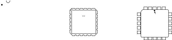
AD7575
DIP/SOIC
|
|
|
|
|
|
VDD |
CS |
1 |
|
|
|
18 |
|
RD |
|
|
|
|
|
VREF |
2 |
|
|
|
17 |
||
TP |
|
|
|
|
|
AIN |
3 |
|
|
|
16 |
||
|
|
|
|
|
|
AGND |
BUSY |
4 |
AD7575 |
15 |
|||
CLK |
|
|
DB0 (LSB) |
|||
5 |
TOP VIEW |
14 |
||||
DB7 (MSB) |
|
(Not to Scale) |
|
DB1 |
||
6 |
|
|
|
13 |
||
DB6 |
|
|
|
|
|
DB2 |
7 |
|
|
|
12 |
||
DB5 |
|
|
|
|
|
DB3 |
8 |
|
|
|
11 |
||
DGND |
|
|
|
|
|
DB4 |
9 |
|
|
|
10 |
||
|
|
|
|
|
|
|
PIN CONFIGURATIONS |
|
|
|
|
|
|
|
|
|
|
|
|
|
|
|
||||||
|
|
LCCC |
|
|
|
|
|
|
|
PLCC |
|
|
|
|
|||||||
|
TP |
RD |
CS |
DD |
REF |
|
|
|
|
RD |
|
CS |
NC |
|
DD |
REF |
|
|
|||
|
V |
V |
|
|
|
|
|
|
V |
V |
|
|
|||||||||
|
3 |
2 |
1 |
20 |
19 |
|
|
3 |
2 |
|
1 |
20 |
|
19 |
|
|
|
||||
|
|
|
|
|
|
|
|
|
|
|
|
|
|||||||||
|
|
|
|
|
|
|
|
|
|
|
|
|
|
|
|
|
|
|
|
|
|
BUSY 4 |
|
|
|
|
|
18 AIN |
TP |
4 |
|
|
|
|
|
|
PIN 1 |
|
|
18 |
AIN |
||
|
|
|
|
|
|
|
|
|
|
|
|||||||||||
CLK 5 |
|
AD7575 |
|
17 AGND |
BUSY |
5 |
|
|
|
|
|
|
IDENTIFIER |
17 |
AGND |
||||||
|
|
|
|
|
AD7575 |
|
|
||||||||||||||
DB7 (MSB) 6 |
|
|
16 DB0 (LSB) |
|
|
|
|
|
|
|
|
|
|||||||||
|
TOP VIEW |
|
CLK |
6 |
|
|
|
|
|
16 |
DB0 (LSB) |
||||||||||
|
|
|
|
|
TOP VIEW |
|
|
||||||||||||||
|
|
|
|
|
|
|
|
|
|||||||||||||
DB6 7 |
(Not to Scale) |
15 DB1 |
|
|
|
|
|
|
|
|
|
||||||||||
DB7 (MSB) |
7 |
|
|
(Not to Scale) |
15 |
DB1 |
|||||||||||||||
DB5 8 |
|
|
|
|
|
14 DB2 |
|
|
|||||||||||||
|
|
|
|
|
DB6 |
8 |
|
|
|
|
|
|
|
|
|
|
|
14 |
DB2 |
||
|
|
|
|
|
|
|
|
|
|
|
|
|
|
|
|
|
|
||||
|
9 |
10 |
11 |
12 |
13 |
|
|
|
|
|
|
|
|
|
|
|
|
|
|
|
|
|
|
|
|
|
9 |
|
10 |
|
11 |
|
12 |
|
13 |
|
|
|
|||||
|
DGND |
NC |
NC |
DB4 |
DB3 |
|
|
|
|
|
|
|
|
|
|
|
|||||
|
|
|
|
|
|
|
|
|
|
|
|
|
|
|
|
|
|||||
|
|
|
|
|
DB5 |
|
DGND |
NC |
|
DB4 |
DB3 |
|
|
||||||||
NC = NO CONNECT |
|
|
|
|
|
NC = NO CONNECT |
|
|
|
|
|
|
|
|
|
|
|
||||
|
|
|
|
|
|
|
|
|
|
|
|
|
|
|
|
|
|
||||
ORDERING GUIDE
|
|
Relative |
|
|
Temperature |
Accuracy |
Package |
Model1 |
Range |
(LSB) |
Options2 |
AD7575JR |
0°C to +70°C |
±1 max |
R-18 |
AD7575JN |
0°C to +70°C |
±1 max |
N-18 |
AD7575KN |
0°C to +70°C |
±1/2 max |
N-18 |
AD7575JP |
0°C to +70°C |
±1 max |
P-20A |
AD7575KP |
0°C to +70°C |
±1/2 max |
P-20A |
AD7575AQ |
–25°C to +85°C |
±1 max |
Q-18 |
AD7575BQ |
–25°C to +85°C |
±1/2 max |
Q-18 |
AD7575SQ |
–55°C to +125°C |
±1 max |
Q-18 |
AD7575TQ |
–55°C to +125°C |
±1/2 max |
Q-18 |
AD7575SE |
–55°C to +125°C |
±1 max |
E-20A |
AD7575TE |
–55°C to +125°C |
±1/2 max |
E-20A |
NOTES
1To order MIL-STD-883, Class B process parts, add /883B to part number. Contact local sales office for military data sheet. For U.S. Standard Military Drawing (SMD), see DESC drawing #5962-87762.
2E = Leadless Ceramic Chip Carrier; N = Plastic DIP; P = Plastic Leaded Chip Carrier; Q = Cerdip, R = SOIC.
TERMINOLOGY
LEAST SIGNIFICANT BIT (LSB)
An ADC with 8-bits resolution can resolve 1 part in 28 (i.e., 256) of full scale. For the AD7575 with +2.46 V full-scale one LSB is 9.61 mV.
TOTAL UNADJUSTED ERROR
This is a comprehensive specification that includes full-scale error, relative accuracy and offset error.
RELATIVE ACCURACY
Relative Accuracy is the deviation of the ADC’s actual code transition points from a straight line drawn between the devices measured first LSB transition point and the measured full-scale transition point.
SNR
Signal-to-Noise Ratio (SNR) is the ratio of the desired signal to the noise produced in the sampled and digitized analog signal. SNR is dependent on the number of quantization levels used in the digitization process; the more levels, the smaller the quantization noise. The theoretical SNR for a sine wave input is given by
SNR = (6.02 N + 1.76) dB
where N is the number of bits in the ADC.
FULL-SCALE ERROR (GAIN ERROR)
The gain of a unipolar ADC is defined as the difference between the analog input levels required to produce the first and the last digital output code transitions. Gain error is a measure of the deviation of the actual span from the ideal span of FS – 2 LSBs.
ANALOG INPUT RANGE
With VREF = +1.23 V, the maximum analog input voltage range is 0 V to +2.46 V. The output data in LSBs is related to the analog input voltage by the integer value of the following expression:
256 |
AIN |
||
Data (LSBs) = |
|
|
+ 0.5 |
2 V |
|
||
REF
SLEW RATE
Slew Rate is the maximum allowable rate of change of input signal such that the digital sample values are not in error. Slew Rate limitations may restrict the analog signal bandwidth for full-scale analog signals below the bandwidth allowed from sampling theorem considerations.
–4– |
REV. B |
Loading...