


 Loading...
Analog Devices AD797BR-REEL7, AD797BR-REEL, AD797BR, AD797BN, AD797AR-REEL7 Datasheet
...a |
Ultralow Distortion, |
Ultralow Noise Op Amp |
FEATURES
Low Noise
0.9 nV/ÖHz typ (1.2 nV/ÖHz max) Input Voltage
Noise at 1 kHz
50 nV p-p Input Voltage Noise, 0.1 Hz to 10 Hz Low Distortion
–120 dB Total Harmonic Distortion at 20 kHz Excellent AC Characteristics
800 ns Settling Time to 16 Bits (10 V Step) 110 MHz Gain Bandwidth (G = 1000)
8 MHz Bandwidth (G = 10)
280 kHz Full Power Bandwidth at 20 V p-p 20 V/ms Slew Rate
Excellent DC Precision
80 mV max Input Offset Voltage
1.0 mV/8C VOS Drift
Specified for 65 V and 615 V Power Supplies
High Output Drive Current of 50 mA
APPLICATIONS
Professional Audio Preamplifiers
IR, CCD, and Sonar Imaging Systems
Spectrum Analyzers
Ultrasound Preamplifiers
Seismic Detectors
SD ADC/DAC Buffers
PRODUCT DESCRIPTION
The AD797 is a very low noise, low distortion operational amplifier ideal for use as a preamplifier. The low noise of 0.9 nV/ÖHz and low total harmonic distortion of –120 dB at audio bandwidths give the AD797 the wide dynamic range
|
5 |
Hz |
4 |
|
|
– nV/ |
|
NOISE |
3 |
VOLTAGE |
2 |
|
|
INPUT |
1 |
|
|
|
0 |
10 |
100 |
1k |
10k |
100k |
1M |
10M |
FREQUENCY – Hz
AD797 Voltage Noise Spectral Density
*Patent pending.
REV. C
Information furnished by Analog Devices is believed to be accurate and reliable. However, no responsibility is assumed by Analog Devices for its use, nor for any infringements of patents or other rights of third parties which may result from its use. No license is granted by implication or otherwise under any patent or patent rights of Analog Devices.
AD797*
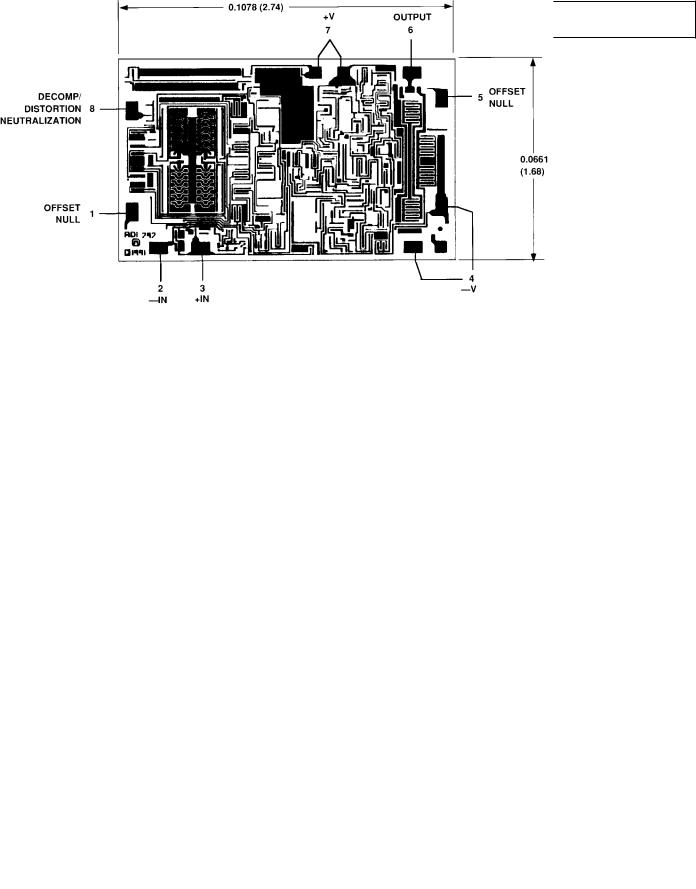
CONNECTION DIAGRAM
8-Pin Plastic Mini-DIP (N),
Cerdip (Q) and SOIC (R) Packages
|
|
|
|
|
DECOMPENSATION & |
|
|
|
|
|
DISTORTION |
OFFSET NULL |
1 |
|
|
8 |
|
|
AD797 |
NEUTRALIZATION |
|||
|
|
|
|
||
–IN |
2 |
|
|
7 |
+VS |
|
|
|
|
|
|
+IN |
3 |
|
|
6 |
OUTPUT |
|
|
|
|
|
|
–VS |
4 |
|
TOP VIEW |
5 |
OFFSET NULL |
|
|
|
|||
|
|
|
|
|
|
necessary for preamps in microphones and mixing consoles. Furthermore, the AD797’s excellent slew rate of 20 V/ms and 110 MHz gain bandwidth make it highly suitable for low frequency ultrasound applications.
The AD797 is also useful in IR and Sonar Imaging applications where the widest dynamic range is necessary. The low distortion and 16-bit settling time of the AD797 make it ideal for buffering the inputs to SD ADCs or the outputs of high resolution DACs especially when they are used in critical applications such as seismic detection and spectrum analyzers. Key features such as a 50 mA output current drive and the specified power supply voltage range of ±5 to ±15 volts make the AD797 an excellent general purpose amplifier.
–90
–100  0.001
0.001
THD– dB |
|
|
|
|
|
|
0.0003 |
THD– % |
||
–110 |
|
|
|
|
|
|
|
|||
–120 |
|
|
|
|
|
|
0.0001 |
|
||
|
|
|
|
|
|
|
|
|
|
|
|
|
|
|
|
|
MEASUREMENT |
|
|
|
|
|
|
|
|
|
|
LIMIT |
|
|
|
|
–130 |
|
|
|
|
|
|
|
|
|
|
|
|
|
|
|
|
|
|
|
|
|
100 |
300 |
1k |
3k |
10k |
30k |
100k |
300k |
|
||
|
|
|
|
FREQUENCY – Hz |
|
|
|
|
|
|
THD vs. Frequency
One Technology Way, P.O. Box 9106, Norwood, MA 02062-9106, U.S.A. Tel: 617/329-4700 Fax: 617/326-8703
AD797–SPECIFICATIONS (@ TA = +258C and VS = 615 V dc, unless otherwise noted)
|
|
|
|
AD797A/S1 |
AD797B |
|
|
|
|
|
||
Model |
Conditions |
VS |
Min |
Typ |
Max |
Min |
Typ |
Max |
Units |
|||
|
|
|
|
|
|
|
|
|
|
|
|
|
INPUT OFFSET VOLTAGE |
|
±5 V, ± 15 V |
|
25 |
80 |
|
10 |
40 |
mV |
|||
|
TMIN to TMAX |
|
|
50 |
125/180 |
|
30 |
60 |
mV |
|||
Offset Voltage Drift |
|
±5 V, ± 15 V |
|
0.2 |
1.0 |
|
0.2 |
0.6 |
mV/°C |
|||
|
|
|
|
|
|
|
|
|
|
|
|
|
INPUT BIAS CURRENT |
|
±5 V, ± 15 V |
|
0.25 |
1.5 |
|
0.25 |
0.9 |
mA |
|||
|
TMIN to TMAX |
|
|
0.5 |
3.0 |
|
0.25 |
2.0 |
mA |
|||
INPUT OFFSET CURRENT |
|
±5 V, ± 15 V |
|
100 |
400 |
|
80 |
200 |
nA |
|||
|
TMIN to TMAX |
|
|
120 |
600/700 |
|
120 |
300 |
nA |
|||
OPEN-LOOP GAIN |
VOUT = ± 10 V |
±15 V |
|
|
|
|
|
|
|
|
|
|
|
RLOAD = 2 kW |
|
1 |
20 |
|
2 |
20 |
|
V/mV |
|||
|
TMIN to TMAX |
|
1 |
6 |
|
2 |
10 |
|
V/mV |
|||
|
RLOAD = 600 W |
|
1 |
15 |
|
2 |
15 |
|
V/mV |
|||
|
TMIN to TMAX |
|
1 |
5 |
|
2 |
7 |
|
V/mV |
|||
|
@ 20 kHz2 |
|
14000 |
20000 |
|
14000 |
20000 |
|
V/V |
|||
DYNAMIC PERFORMANCE |
|
|
|
|
|
|
|
|
|
|
|
|
Gain Bandwidth Product |
G = 1000 |
±15 V |
|
110 |
|
|
110 |
|
MHz |
|||
|
G = 10002 |
±15 V |
|
450 |
|
|
450 |
|
MHz |
|||
–3 dB Bandwidth |
G = 10 |
±15 V |
|
8 |
|
|
8 |
|
MHz |
|||
Full Power Bandwidth3 |
VO = 20 V p-p, |
|
|
|
|
|
|
|
|
|
|
|
|
RLOAD = 1 kW |
±15 V |
|
280 |
|
|
280 |
|
kHz |
|||
Slew Rate |
RLOAD = 1 kW |
±15 V |
12.5 |
20 |
|
12.5 |
20 |
|
V/ms |
|||
Settling Time to 0.0015% |
10 V Step |
±15 V |
|
800 |
1200 |
|
800 |
1200 |
ns |
|||
|
|
|
|
|
|
|
|
|
|
|
|
|
COMMON-MODE REJECTION |
VCM = CMVR |
±5 V, ± 15 V |
114 |
130 |
|
120 |
130 |
|
dB |
|||
|
TMIN to TMAX |
|
110 |
120 |
|
114 |
120 |
|
dB |
|||
POWER SUPPLY REJECTION |
VS = ±5 V to ± 18 V |
|
114 |
130 |
|
120 |
130 |
|
dB |
|||
|
TMIN to TMAX |
|
110 |
120 |
|
114 |
120 |
|
dB |
|||
INPUT VOLTAGE NOISE |
f = 0. 1 Hz to 10 Hz |
±15 V |
|
50 |
|
|
50 |
|
nV p-p |
|||
|
f = 10 Hz |
±15 V |
|
1.7 |
|
|
1.7 |
2.5 |
nV/Ö |
Hz |
|
|
|
f = 1 kHz |
±15 V |
|
0.9 |
1.2 |
|
0.9 |
1.2 |
nV/Ö |
Hz |
|
|
|
f = 10 Hz–1 MHz |
±15 V |
|
1.0 |
1.3 |
|
1.0 |
1.2 |
mV rms |
|||
|
|
|
|
|
|
|
|
|
|
|||
INPUT CURRENT NOISE |
f = 1 kHz |
±15 V |
|
2.0 |
|
|
2.0 |
|
pA/Ö |
|
|
|
|
|
|
|
Hz |
||||||||
|
|
|
|
|
|
|
|
|
|
|||
INPUT COMMON-MODE |
|
±15 V |
±11 |
±12 |
|
±11 |
±12 |
|
V |
|||
VOLTAGE RANGE |
|
±5 V |
±2.5 |
±3 |
|
±2.5 |
±3 |
|
V |
|||
|
|
|
|
|
|
|
|
|
|
|||
OUTPUT VOLTAGE SWING |
RLOAD = 2 kW |
±15 V |
±12 |
±13 |
|
±12 |
±13 |
|
V |
|||
|
RLOAD = 600 W |
±15 V |
±11 |
±13 |
|
±11 |
±13 |
|
V |
|||
|
RLOAD = 600 W |
±5 V |
±2.5 |
±3 |
|
±2.5 |
±3 |
|
V |
|||
Short-Circuit Current |
|
±5 V, ± 15 V |
|
80 |
|
|
80 |
|
mA |
|||
Output Current4 |
|
±5 V, ± 15 V |
30 |
50 |
|
30 |
50 |
|
mA |
|||
TOTAL HARMONIC DISTORTION |
RLOAD = 1 kW, CN = 50 pF |
±15 V |
|
–98 |
–90 |
|
–98 |
–90 |
dB |
|||
|
f = 250 kHz, 3 V rms |
|
|
|
|
|
|
|
|
|
|
|
|
RLOAD = 1 kW |
±15 V |
|
–120 |
–110 |
|
–120 |
–110 |
dB |
|||
|
f = 20 kHz, 3 V rms |
|
|
|
|
|
|
|
|
|
|
|
|
|
|
|
|
|
|
|
|
|
|
|
|
INPUT CHARACTERISTICS |
|
|
|
|
|
|
|
|
|
|
|
|
Input Resistance (Differential) |
|
|
|
7.5 |
|
|
7.5 |
|
kW |
|||
Input Resistance (Common Mode) |
|
|
|
100 |
|
|
100 |
|
MW |
|||
Input Capacitance (Differential)5 |
|
|
|
20 |
|
|
20 |
|
pF |
|||
Input Capacitance (Common Mode) |
|
|
|
5 |
|
|
5 |
|
pF |
|||
|
|
|
|
|
|
|
|
|
|
|||
OUTPUT RESISTANCE |
AV = +1, f = 1 kHz |
|
|
3 |
|
|
3 |
|
mW |
|||
|
|
|
|
|
|
|
|
|
|
|
|
|
POWER SUPPLY |
|
|
|
|
|
|
|
|
|
|
|
|
Operating Range |
|
±5 V, ± 15 V |
±5 |
|
±18 |
±5 |
|
±18 |
V |
|||
Quiescent Current |
|
|
8.2 |
10.5 |
|
8.2 |
10.5 |
mA |
||||
|
|
|
|
|
|
|
|
|
|
|
|
|
NOTES
1See standard military drawing for 883B specifications.
2Specified using external decompensation capacitor, see Applications section.
3Full Power Bandwidth = Slew Rate/2 π VPEAK. 4Output Current for |VS – VOUT| >4 V, AOL > 200 kΩ.
5Differential input capacitance consists of 1.5 pF package capacitance and 18.5 pF from the input differential pair.
Specifications subject to change without notice.
–2– |
REV. C |
AD797
ABSOLUTE MAXIMUM RATINGS1
Supply Voltage . . . . . . . . . . . . . . . . . . . . . . . . . . . . . . . . ±18 V Internal Power Dissipation @ +25°C2
Input Voltage . . . . . . . . . . . . . . . . . . . . . . . . . . . . . . . . . . .±VS Differential Input Voltage3 . . . . . . . . . . . . . . . . . . . . . . ±0.7 V
Output Short Circuit Duration . . . . . . .Indefinite Within max Internal Power Dissipation Storage Temperature Range (Cerdip) . . . . . . –65°C to +150°C
Storage Temperature Range (N, R Suffix) . . –65°C to +125°C Operating Temperature Range
AD797A/B . . . . . . . . . . . . . . . . . . . . . . . . . –40°C to +85°C AD797S . . . . . . . . . . . . . . . . . . . . . . . . . . –55°C to +125°C Lead Temperature Range (Soldering 60 sec) . . . . . . . +300°C
NOTES
1Stresses above those listed under “Absolute Maximum Ratings” may cause permanent damage to the device. This is a stress rating only, and functional operation of the device at these or any other conditions above those indicated in the operational section of this specification is not implied. Exposure to absolute maximum rating conditions for extended periods may affect device reliability.
2Internal Power Dissipation:
8-Pin SOIC = 0.9 Watts (TA–25°C)/θJA
8-Pin Plastic DIP and Cerdip = 1.3 Watts – (TA–25°C)/θJA Thermal Characteristics
8-Pin Plastic DIP Package: θJA = 95°C/W 8-Pin Cerdip Package: θJA = 110°C/W
8-Pin Small Outline Package: θJA = 155°C/W
3The AD797’s inputs are protected by back-to-back diodes. To achieve low noise, internal current limiting resistors are not incorporated into the design of this amplifier. If the differential input voltage exceeds ± 0.7 V, the input current should be limited to less than 25 mA by series protection resistors. Note, however, that this will degrade the low noise performance of the device.
ESD SUSCEPTIBILITY
ESD (electrostatic discharge) sensitive device. Electrostatic charges as high as 4000 volts, which readily accumulate on the human body and on test equipment, can discharge without detection. Although the AD797 features proprietary ESD protection circuitry, permanent damage may still occur on these devices if they are subjected to high energy electrostatic discharges. Therefore, proper ESD precautions are recommended to avoid any performance degradation or loss of functionality.
ORDERING GUIDE
|
Temperature |
Package |
Package |
Model |
Range |
Description |
Option |
|
|
|
|
AD797AN |
–40°C to +85°C |
8-Pin Plastic DIP |
N-8 |
AD797BN |
–40°C to +85°C |
8-Pin Plastic DIP |
N-8 |
AD797BR |
–40°C to +85°C |
8-Pin Plastic SOIC |
SO-8 |
AD797BR-REEL |
–40°C to +85°C |
8-Pin Plastic SOIC |
SO-8 |
AD797BR-REEL7 |
–40°C to +85°C |
8-Pin Plastic SOIC |
SO-8 |
AD797AR |
–40°C to +85°C |
8-Pin Plastic SOIC |
SO-8 |
AD797AR-REEL |
–40°C to +85°C |
8-Pin Plastic SOIC |
SO-8 |
AD797AR-REEL7 |
–40°C to +85°C |
8-Pin Plastic SOIC |
SO-8 |
5962-9313301MPA |
–55°C to +125°C |
8-Pin Cerdip |
Q-8 |
METALIZATION PHOTO
Contact factory for latest dimensions.
Dimensions shown in inches and (mm).
NOTE
The AD797 has double layer metal. Only one layer is shown here for clarity.
REV. C |
–3– |
AD797–Typical Characteristics
±Volts– |
20 |
|
|
|
|
|
|
15 |
|
|
|
|
|
|
|
RANGE |
|
|
|
|
|
|
|
|
|
|
|
|
|
|
|
MODE-COMMON |
10 |
|
|
|
|
|
|
|
|
|
|
|
|
|
|
INPUT |
5 |
|
|
|
|
|
|
|
|
|
|
|
|
|
|
|
0 |
|
|
|
|
|
|
|
|
5 |
10 |
15 |
20 |
||
|
0 |
||||||
SUPPLY VOLTAGE – ±Volts
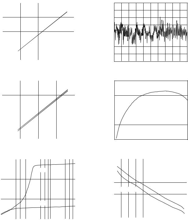
Figure 1. Common-Mode Voltage Range vs. Supply
±Volts |
20 |
|
|
|
|
|
|
|
15 |
|
|
|
|
|
|
|
|
–SWING |
|
|
|
|
|
|
|
|
|
|
|
–VOUT |
|
|
|
|
|
VOLTAGE |
10 |
|
|
|
|
|
|
|
|
|
|
|
|
|
|
|
|
OUTPUT |
|
|
|
|
+VOUT |
|
|
|
5 |
|
|
|
|
|
|
|
|
|
|
|
|
|
|
|
|
|
|
0 |
|
|
|
|
|
|
|
|
|
5 |
10 |
15 |
20 |
|||
|
0 |
|||||||
|
|
|
|
SUPPLY VOLTAGE – ±Volts |
|
|
|
|
|
Figure 2. Output Voltage Swing vs. Supply |
|
|
|||||
p-p |
30 |
|
|
|
|
|
|
|
|
|
|
VS = ±15V |
|
|
|
||
|
|
|
|
|
|
|
||
Volts– |
|
|
|
|
|
|
|
|
20 |
|
|
|
|
|
|
|
|
SWINGVOLTAGE |
|
|
|
|
|
|
|
|
10 |
|
|
|
|
|
|
|
|
OUTPUT |
|
|
|
|
VS = ±5V |
|
|
|
|
|
|
|
|
|
|
|
|
|
0 |
|
|
|
|
|
|
|
|
|
|
|
|
|
|
|
|
|
10 |
100 |
1k |
|
10k |
|||
LOAD RESISTANCE – Ω
Figure 3. Output Voltage Swing vs. Load Resistance
0.01 V/DIV |
VERTICAL SCALE – |
HORIZONTAL SCALE – 5 sec/DIV |
Figure 4. 0.1 Hz to 10 Hz Noise
0.0
A |
–0.5 |
CURRENT – |
–1.0 |
INPUT BIAS |
–1.5 |
|
–2.0 |
|
–60 |
–40 |
–20 |
0 |
20 |
40 |
60 |
80 |
100 |
120 |
140 |
||||
|
|
|
|
|
|
TEMPERATURE – °C |
|
|
|
|
|
|
|||
|
Figure 5. Input Bias Current vs. Temperature |
||||||||||||||
mA– |
140 |
|
|
|
|
|
|
|
|
|
|
|
|
|
|
|
|
|
|
|
|
|
|
|
|
|
|
|
|
||
120 |
|
|
|
|
|
|
|
|
|
|
|
|
|
|
|
CURRENT |
100 |
|
|
|
|
|
|
SOURCE CURRENT |
|
|
|
|
|||
CIRCUITSHORT |
60 |
|
SINK CURRENT |
|
|
|
|
|
|
|
|
|
|
||
|
|
|
|
|
|
|
|
|
|
|
|||||
|
|
|
|
|
|
|
|
|
|
|
|
|
|
||
|
80 |
|
|
|
|
|
|
|
|
|
|
|
|
|
|
|
40 |
|
|
|
|
|
|
|
|
|
|
|
|
|
|
|
|
|
|
|
|
|
|
|
|
|
|
|
|
|
|
|
–60 |
–40 |
–20 |
0 |
20 |
40 |
60 |
80 |
100 |
120 |
140 |
||||
|
|
|
|
|
|
TEMPERATURE – °C |
|
|
|
|
|
|
|||
Figure 6. Short Circuit Current vs. Temperature
–4– |
REV. C |

mA– |
11 |
|
|
|
|
|
10 |
|
+125°C |
|
|
|
|
CURRENT |
9 |
|
|
|
|
|
SUPPLY |
8 |
|
+25°C |
|
|
|
QUIESCENT |
7 |
|
|
|
|
|
|
|
|
|
|
|
|
|
|
|
–55°C |
|
|
|
|
6 |
|
|
|
|
|
|
|
|
|
|
|
|
|
0 |
5 |
10 |
15 |
20 |
|
SUPPLY VOLTAGE – ±Volts
Figure 7. Quiescent Supply Current vs. Supply Voltage
|
12 |
|
FREQ = 1kHz |
|
|
|
|
|
|
|
|
|
|
|
|
rms |
|
|
RL = 600W |
|
|
|
|
9 |
|
G = +10 |
|
|
|
|
|
|
|
|
|
|
|
||
Volts– |
|
|
|
|
|
|
|
|
|
|
|
|
|
|
|
VOLTAGE |
6 |
|
|
|
|
|
|
|
|
|
|
|
|
|
|
OUTPUT |
3 |
|
|
|
|
|
|
|
|
|
|
|
|
|
|
|
0 |
|
|
|
|
|
|
|
|
|
|
|
|
|
|
|
0 |
±5 |
±10 |
±15 |
±20 |
||
SUPPLY VOLTAGE – Volts
Figure 8. Output Voltage vs. Supply for 0.01% Distortion
|
1.0 |
|
|
|
|
|
|
0.8 |
|
|
|
|
|
s |
|
|
|
0.0015% |
|
|
|
|
|
|
|
|
|
– |
0.6 |
|
|
|
|
|
TIME |
|
|
|
|
|
|
|
|
|
|
|
|
|
SETTLING |
|
|
|
|
0.01% |
|
|
|
|
|
|
|
|
|
0.4 |
|
|
|
|
|
|
0.2 |
|
|
|
|
|
|
0.0 |
|
|
|
|
|
|
0 |
2 |
4 |
6 |
8 |
10 |
|
|
|
STEP SIZE – Volts |
|
|
|
Figure 9. Settling Time vs. Step Size (±)
|
|
|
|
|
|
|
AD797 |
|
||
dB– |
140 |
|
|
|
|
|
|
|
|
|
|
|
|
|
|
|
|
|
|
||
120 |
|
|
|
|
PSR |
|
|
|
|
|
REJECTIONSUPPLYPOWER |
|
|
|
|
|
+SUPPLY |
|
|
|
dB–REJECTIONMODECOMMON |
100 |
|
|
PSR |
|
|
|
150 |
|||
|
|
|
–SUPPLY |
|
|
|
|
|
||
|
80 |
|
|
|
|
|
|
|
125 |
|
|
|
|
|
|
|
CMR |
|
|
|
|
|
60 |
|
|
|
|
|
|
|
100 |
|
|
40 |
|
|
|
|
|
|
|
75 |
|
|
20 |
|
|
|
|
|
|
|
50 |
|
|
|
|
|
|
|
|
|
|
||
|
1 |
10 |
100 |
1k |
10k |
100k |
1M |
|
||
FREQUENCY – Hz
Figure 10. Power Supply and Common-Mode Rejection vs. Frequency
|
–60 |
|
RL = 600 W |
|
|
|
|
|
|
|
|
|
|
|
|
|
G = +10 |
|
|
|
|
|
|
FREQ = 10kHz |
|
|
|
NOISEdB– |
|
|
NOISE BW = 100kHz |
|
|
|
–80 |
|
|
|
|
|
|
|
|
|
|
|
|
|
+ |
|
|
V |
= ±5V |
|
|
|
|
S |
|
|
|
|
THD |
–100 |
|
|
|
|
|
|
|
|
|
|
|
|
|
|
|
|
|
VS = ±15V |
|
|
–120 |
|
|
|
|
|
|
|
|
|
|
|
|
|
0.01 |
0.1 |
1.0 |
10 |
||
OUTPUT LEVEL – Volts
Figure 11. Total Harmonic Distortion (THD) + Noise vs. Output Level
30
±15V SUPPLIES
RL = 600 Ω
20
10 |
|
|
|
|
±5V SUPPLIES |
|
|
0 |
|
|
|
10k |
100k |
1M |
10M |
Figure 12. Large Signal Frequency Response
REV. C |
–5– |
Loading...