


 Loading...
2-Channel, 500 MSPS DDS with 10-Bit DACs AD9958
FEATURES |
APPLICATIONS |
2 synchronized DDS channels @ 500 MSPS |
Agile local oscillators |
Independent frequency/phase/amplitude control between |
Phased array radars/sonars |
channels |
Instrumentation |
Matched latencies for frequency/phase/amplitude changes |
Synchronized clocking |
Excellent channel-to-channel isolation (>72 dB) |
RF source for AOTF |
Linear frequency/phase/amplitude sweeping capability |
Single-side band suppressed carriers |
Up to 16 levels of frequency/phase/amplitude modulation |
Quadrature communications |
(pin-selectable) |
|
2 integrated 10-bit digital-to-analog converters (DACs) |
|
Individually programmable DAC full-scale currents |
|
0.12 Hz or better frequency tuning resolution |
|
14-bit phase offset resolution |
|
10-bit output amplitude scaling resolution |
|
Serial I/O port interface (SPI) with 800 Mbps data throughput |
|
Software-/hardware-controlled power-down |
|
Dual supply operation (1.8 V DDS core/3.3 V serial I/O) |
|
Multiple device synchronization |
|
Selectable 4× to 20× REFCLK multiplier (PLL) |
|
Selectable REFCLK crystal oscillator |
|
56-lead LFCSP |
|
|
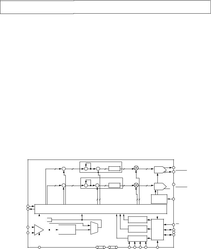
FUNCTIONAL BLOCK DIAGRAM |
|
||
|
AD9958 |
(2) |
10-BIT |
RECONSTRUCTED |
|
DAC |
SINE WAVE |
||
|
|
500MSPS |
|
|
|
|
DDS CORES |
10-BIT |
RECONSTRUCTED |
|
|
DAC |
SINE WAVE |
|
|
MODULATION CONTROL |
|
|
|
SYSTEM |
REF CLOCK |
TIMING AND |
|
|
CLOCK |
INPUT CIRCUITRY |
CONTROL |
|
|
SOURCE |
|
|
|
05252-000 |
|
|
USER INTERFACE |
|
|
|
|
|
|
|
Figure 1.
Rev. A
Information furnished by Analog Devices is believed to be accurate and reliable. However, no responsibilityisassumedbyAnalogDevicesforitsuse,norforanyinfringementsofpatentsorother rightsofthirdpartiesthatmayresultfromitsuse.Specificationssubjecttochangewithoutnotice.No license is granted by implication or otherwise under any patent or patent rights of Analog Devices. Trademarksandregisteredtrademarksarethepropertyoftheirrespectiveowners.
One Technology Way, P.O. Box 9106, Norwood, MA 02062-9106, U.S.A. Tel: 781.329.4700 www.analog.com Fax: 781.461.3113 © 2005–2008 Analog Devices, Inc. All rights reserved.

AD9958
TABLE OF CONTENTS |
|
Features .............................................................................................. |
1 |
Applications....................................................................................... |
1 |
Functional Block Diagram .............................................................. |
1 |
General Description ......................................................................... |
3 |
Specifications..................................................................................... |
4 |
Absolute Maximum Ratings............................................................ |
8 |
ESD Caution.................................................................................. |
8 |
Pin Configuration and Function Descriptions............................. |
9 |
Typical Performance Characteristics ........................................... |
11 |
Application Circuits ....................................................................... |
14 |
Equivalent Input and Output Circuits ......................................... |
17 |
Theory of Operation ...................................................................... |
18 |
DDS Core..................................................................................... |
18 |
Digital-to-Analog Converter .................................................... |
18 |
Modes of Operation ....................................................................... |
19 |
Channel Constraint Guidelines ................................................ |
19 |
Power Supplies ............................................................................ |
19 |
Single-Tone Mode ...................................................................... |
19 |
Reference Clock Modes ............................................................. |
20 |
Scalable DAC Reference Current Control Mode ................... |
21 |
Power-Down Functions............................................................. |
21 |
Modulation Mode....................................................................... |
21 |
Modulation Using SDIO_x Pins for RU/RD........................... |
24 |
REVISION HISTORY |
|
7/08—Rev. 0 to Rev. A |
|
Changes to Features.......................................................................... |
1 |
Inserted Figure 1; Renumbered Sequentially................................ |
1 |
Changes to Input Level Parameter in Table 1 ............................... |
4 |
Added Profile Pin Toggle Rate Parameter in Table 1................... |
6 |
Changes to Layout ............................................................................ |
8 |
Changes to Table 3............................................................................ |
9 |
Added Equivalent Input and Output Circuits Section .............. |
17 |
Changes to Reference Clock Input Circuitry Section................ |
20 |
Change to Figure 35 ....................................................................... |
21 |
Changes to Setting the Slope of the Linear Sweep Section ....... |
25 |
Changes to Figure 37...................................................................... |
26 |
Changes to Figure 38 and Figure 39............................................. |
27 |
Changes to Figure 40...................................................................... |
30 |
Linear Sweep Mode.................................................................... |
25 |
Linear Sweep No-Dwell Mode ................................................. |
26 |
Sweep and Phase Accumulator Clearing Functions.............. |
27 |
Output Amplitude Control Mode............................................ |
28 |
Synchronizing Multiple AD9958 Devices................................... |
29 |
Automatic Mode Synchronization........................................... |
29 |
Manual Software Mode Synchronization................................ |
29 |
Manual Hardware Mode Synchronization.............................. |
29 |
I/O_UPDATE, SYNC_CLK, and System Clock |
|
Relationships............................................................................... |
30 |
Serial I/O Port................................................................................. |
31 |
Overview ..................................................................................... |
31 |
Instruction Byte Description .................................................... |
32 |
Serial I/O Port Pin Description................................................ |
32 |
Serial I/O Port Function Description ...................................... |
32 |
MSB/LSB Transfer Description ................................................ |
32 |
Serial I/O Modes of Operation................................................. |
33 |
Register Maps and Bit Descriptions............................................. |
36 |
Register Maps.............................................................................. |
36 |
Descriptions for Control Registers .......................................... |
39 |
Descriptions for Channel Registers ......................................... |
41 |
Outline Dimensions ....................................................................... |
44 |
Ordering Guide .......................................................................... |
44 |
Added Table 25; Renumbered Sequentially ................................ |
31 |
Changes to Figure 41...................................................................... |
31 |
Changes to Figure 42, Serial Data I/O (SDIO_0, SDIO_1, |
|
SDIO_3) Section, and Added Example Instruction Byte |
|
Section.............................................................................................. |
32 |
Added Table 27 ............................................................................... |
33 |
Changes to Figure 46, Figure 47, Figure 48, and Figure 49....... |
35 |
Changes to Register Maps and Bit Descriptions Section and |
|
Added Endnote 2 to Table 28........................................................ |
36 |
Added Endnote 1 to Table 30........................................................ |
38 |
Added Exposed Pad Notation to Outline Dimensions ............. |
44 |
9/05—Revision 0: Initial Version |
|
Rev. A | Page 2 of 44
AD9958
GENERAL DESCRIPTION
The AD9958 consists of two DDS cores that provide independent frequency, phase, and amplitude control on each channel. This flexibility can be used to correct imbalances between signals due to analog processing, such as filtering, amplification, or PCB layout related mismatches. Because both channels share a common system clock, they are inherently synchronized. Synchronization of multiple devices is supported.
The AD9958 can perform up to a 16-level modulation of frequency, phase, or amplitude (FSK, PSK, ASK). Modulation is performed by applying data to the profile pins. In addition, the AD9958 also supports linear sweep of frequency, phase, or amplitude for applications such as radar and instrumentation.
The AD9958 serial I/O port offers multiple configurations to provide significant flexibility. The serial I/O port offers an SPIcompatible mode of operation that is virtually identical to the SPI operation found in earlier Analog Devices, Inc., DDS products. Flexibility is provided by four data pins (SDIO_0/ SDIO_1/SDIO_2/SDIO_3) that allow four programmable modes of serial I/O operation.
The AD9958 uses advanced DDS technology that provides low power dissipation with high performance. The device incorporates two integrated, high speed 10-bit DACs with excellent wideband and narrow-band SFDR. Each channel has a dedicated 32-bit frequency tuning word, 14 bits of phase offset, and a 10-bit output scale multiplier.
The DAC outputs are supply referenced and must be terminated into AVDD by a resistor or an AVDD center-tapped transformer. Each DAC has its own programmable reference to enable different full-scale currents for each channel.
The DDS acts as a high resolution frequency divider with the REFCLK as the input and the DAC providing the output. The REFCLK input source is common to both channels and can be driven directly or used in combination with an integrated REFCLK multiplier (PLL) up to a maximum of 500 MSPS. The PLL multiplication factor is programmable from 4 to 20, in integer steps. The REFCLK input also features an oscillator circuit to support an external crystal as the REFCLK source. The crystal must be between 20 MHz and 30 MHz. The crystal can be used in combination with the REFCLK multiplier.
The AD9958 comes in a space-saving 56-lead LFCSP package. The DDS core (AVDD and DVDD pins) is powered by a 1.8 V supply. The digital I/O interface (SPI) operates at 3.3 V and requires the pin labeled DVDD_I/O (Pin 49) be connected
to 3.3 V.
The AD9958 operates over the industrial temperature range of −40°C to +85°C.
AD9958
Σ
32 32
Σ
32 32
FTW 32
32
FTW
SYNC_IN
SYNC_OUT
I/O_UPDATE

SYNC_CLK
 ÷4
÷4
REF_CLK |
|
|
|
|
|
|
REF CLOCK |
|
|
|
|
|
|
|
|||
|
|
|
|
|
|
|||
|
|
|
|
|
|
|
|
MULTIPLIER |
|
|
|
|
|
|
|
|
4× TO 20× |
REF_CLK |
|
|
|
BUFFER/ |
||||
|
|
|
|
|||||
|
|
|
|
|
XTAL |
|
||
|
|
|
|
|
OSCILLATOR |
|
||
|
|
|
|
|
|
|
||
|
|
CLK_MODE_SEL |
|
|||||
|
|
DDS CORE |
|
|
|
|
|
Σ |
Σ |
15 COS(X) |
10 |
10 |
DAC |
CH0_IOUT |
|
CH0_IOUT |
|||||||
|
|
|
|
|
|
|
|
DDS CORE |
|
|
Σ |
Σ |
15 COS(X) |
10 |
|
PHASE/ |
14 |
|
AMP/ |
10 |
PHASE |
|
|
AMP |
|
TIMING AND CONTROL LOGIC
SYSTEM
CLK
MUX
1.8V 1.8V
CONTROL REGISTERS
CHANNEL REGISTERS
PROFILE REGISTERS
 CH1_IOUT 10 DAC
 CH1_IOUT
SCALABLE
DAC REF DAC_RSET
CURRENT

 PWR_DWN_CTL
 MASTER_RESET

 SCLK
SCLK
CS
I/O
PORT SDIO_0
BUFFER 
 SDIO_1
SDIO_2

 SDIO_3
|
|
|
|
|
AVDD |
DVDD |
P0 P1 P2 P3 DVDD_I/O |
||
Figure 2. Detailed Block Diagram
05252-001
Rev. A | Page 3 of 44

AD9958
SPECIFICATIONS
AVDD and DVDD = 1.8 V ± 5%; DVDD_I/O = 3.3 V ± 5%; T = 25°C; RSET = 1.91 kΩ; external reference clock frequency = 500 MSPS (REFCLK multiplier bypassed), unless otherwise noted.
Table 1.
Parameter |
Min |
Typ |
Max |
Unit |
Test Conditions/Comments |
REFERENCE CLOCK INPUT CHARACTERISTICS |
|
|
|
|
See Figure 34 and Figure 35 |
Frequency Range |
|
|
|
|
|
REFCLK Multiplier Bypassed |
1 |
|
500 |
MHz |
|
REFCLK Multiplier Enabled |
10 |
|
125 |
MHz |
|
Internal VCO Output Frequency Range |
|
|
|
|
|
VCO Gain Control Bit Set High1 |
255 |
|
500 |
MHz |
|
VCO Gain Control Bit Set Low1 |
100 |
|
160 |
MHz |
|
Crystal REFCLK Source Range |
20 |
|
30 |
MHz |
|
Input Level |
200 |
|
1000 |
mV |
Measured at each pin (single-ended) |
Input Voltage Bias Level |
|
1.15 |
|
V |
|
Input Capacitance |
|
2 |
|
pF |
|
Input Impedance |
|
1500 |
|
Ω |
|
Duty Cycle with REFCLK Multiplier Bypassed |
45 |
|
55 |
% |
|
Duty Cycle with REFCLK Multiplier Enabled |
35 |
|
65 |
% |
|
CLK Mode Select (Pin 24) Logic 1 Voltage |
1.25 |
|
1.8 |
V |
1.8 V digital input logic |
CLK Mode Select (Pin 24) Logic 0 Voltage |
|
|
0.5 |
V |
1.8 V digital input logic |
DAC OUTPUT CHARACTERISTICS |
|
|
|
|
Must be referenced to AVDD |
Resolution |
|
|
10 |
Bits |
|
Full-Scale Output Current |
1.25 |
|
10 |
mA |
|
Gain Error |
−10 |
|
+10 |
% FS |
|
Channel-to-Channel Output Amplitude Matching Error |
−2.5 |
|
+2.5 |
% |
|
Output Current Offset |
|
1 |
25 |
μA |
|
Differential Nonlinearity |
|
±0.5 |
|
LSB |
|
Integral Nonlinearity |
|
±1.0 |
|
LSB |
|
Output Capacitance |
|
3 |
|
pF |
|
Voltage Compliance Range |
AVDD − |
|
AVDD + |
V |
|
|
0.50 |
|
0.50 |
|
|
Channel-to-Channel Isolation |
72 |
|
|
dB |
DAC supplies tied together (see Figure 19) |
|
|
|
|
|
|
WIDEBAND SFDR |
|
|
|
|
The frequency range for wideband SFDR |
|
|
|
|
|
is defined as dc to Nyquist |
1 MHz to 20 MHz Analog Output |
|
−65 |
|
dBc |
|
20 MHz to 60 MHz Analog Output |
|
−62 |
|
dBc |
|
60 MHz to 100 MHz Analog Output |
|
−59 |
|
dBc |
|
100 MHz to 150 MHz Analog Output |
|
−56 |
|
dBc |
|
150 MHz to 200 MHz Analog Output |
|
−53 |
|
dBc |
|
NARROW-BAND SFDR |
|
|
|
|
|
1.1 MHz Analog Output (±10 kHz) |
|
−90 |
|
dBc |
|
1.1 MHz Analog Output (±50 kHz) |
|
−88 |
|
dBc |
|
1.1 MHz Analog Output (±250 kHz) |
|
−86 |
|
dBc |
|
1.1 MHz Analog Output (±1 MHz) |
|
−85 |
|
dBc |
|
15.1 MHz Analog Output (±10 kHz) |
|
−90 |
|
dBc |
|
15.1 MHz Analog Output (±50 kHz) |
|
−87 |
|
dBc |
|
15.1 MHz Analog Output (±250 kHz) |
|
−85 |
|
dBc |
|
15.1 MHz Analog Output (±1 MHz) |
|
−83 |
|
dBc |
|
40.1 MHz Analog Output (±10 kHz) |
|
−90 |
|
dBc |
|
40.1 MHz Analog Output (±50 kHz) |
|
−87 |
|
dBc |
|
40.1 MHz Analog Output (±250 kHz) |
|
−84 |
|
dBc |
|
40.1 MHz Analog Output (±1 MHz) |
|
−82 |
|
dBc |
|
75.1 MHz Analog Output (±10 kHz) |
|
−87 |
|
dBc |
|
|
|
|
|
|
|
Rev. A | Page 4 of 44

|
|
|
|
|
|
AD9958 |
|
|
|
|
|
|
|
|
|
|
|
|
|
|
Parameter |
Min |
Typ |
Max |
Unit |
Test Conditions/Comments |
|
|
|
|
|
|
|
|
75.1 MHz Analog Output (±50 kHz) |
|
−85 |
|
dBc |
|
|
75.1 MHz Analog Output (±250 kHz) |
|
−83 |
|
dBc |
|
|
75.1 MHz Analog Output (±1 MHz) |
|
−82 |
|
dBc |
|
|
100.3 MHz Analog Output (±10 kHz) |
|
−87 |
|
dBc |
|
|
100.3 MHz Analog Output (±50 kHz) |
|
−85 |
|
dBc |
|
|
100.3 MHz Analog Output (±250 kHz) |
|
−83 |
|
dBc |
|
|
100.3 MHz Analog Output (±1 MHz) |
|
−81 |
|
dBc |
|
|
200.3 MHz Analog Output (±10 kHz) |
|
−87 |
|
dBc |
|
|
200.3 MHz Analog Output (±50 kHz) |
|
−85 |
|
dBc |
|
|
200.3 MHz Analog Output (±250 kHz) |
|
−83 |
|
dBc |
|
|
200.3 MHz Analog Output (±1 MHz) |
|
−81 |
|
dBc |
|
|
|
|
|
|
|
|
|
PHASE NOISE CHARACTERISTICS |
|
|
|
|
|
|
Residual Phase Noise @ 15.1 MHz (fOUT) |
|
|
|
|
|
|
@ 1 kHz Offset |
|
−150 |
|
dBc/Hz |
|
|
@ 10 kHz Offset |
|
−159 |
|
dBc/Hz |
|
|
@ 100 kHz Offset |
|
−165 |
|
dBc/Hz |
|
|
@ 1 MHz Offset |
|
−165 |
|
dBc/Hz |
|
|
Residual Phase Noise @ 40.1 MHz (fOUT) |
|
|
|
|
|
|
@ 1 kHz Offset |
|
−142 |
|
dBc/Hz |
|
|
@ 10 kHz Offset |
|
−151 |
|
dBc/Hz |
|
|
@ 100 kHz Offset |
|
−160 |
|
dBc/Hz |
|
|
@ 1 MHz Offset |
|
−162 |
|
dBc/Hz |
|
|
Residual Phase Noise @ 75.1 MHz (fOUT) |
|
|
|
|
|
|
@ 1 kHz Offset |
|
−135 |
|
dBc/Hz |
|
|
@ 10 kHz Offset |
|
−146 |
|
dBc/Hz |
|
|
@ 100 kHz Offset |
|
−154 |
|
dBc/Hz |
|
|
@ 1 MHz Offset |
|
−157 |
|
dBc/Hz |
|
|
Residual Phase Noise @ 100.3 MHz (fOUT) |
|
|
|
|
|
|
@ 1 kHz Offset |
|
−134 |
|
dBc/Hz |
|
|
@ 10 kHz Offset |
|
−144 |
|
dBc/Hz |
|
|
@ 100 kHz Offset |
|
−152 |
|
dBc/Hz |
|
|
@ 1 MHz Offset |
|
−154 |
|
dBc/Hz |
|
|
Residual Phase Noise @ 15.1 MHz (fOUT) with REFCLK |
|
|
|
|
|
|
Multiplier Enabled 5× |
|
|
|
|
|
|
@ 1 kHz Offset |
|
−139 |
|
dBc/Hz |
|
|
@ 10 kHz Offset |
|
−149 |
|
dBc/Hz |
|
|
@ 100 kHz Offset |
|
−153 |
|
dBc/Hz |
|
|
@ 1 MHz Offset |
|
−148 |
|
dBc/Hz |
|
|
Residual Phase Noise @ 40.1 MHz (fOUT) with REFCLK |
|
|
|
|
|
|
Multiplier Enabled 5× |
|
|
|
|
|
|
@ 1 kHz Offset |
|
−130 |
|
dBc/Hz |
|
|
@ 10 kHz Offset |
|
−140 |
|
dBc/Hz |
|
|
@ 100 kHz Offset |
|
−145 |
|
dBc/Hz |
|
|
@ 1 MHz Offset |
|
−139 |
|
dBc/Hz |
|
|
Residual Phase Noise @ 75.1 MHz (fOUT) with REFCLK |
|
|
|
|
|
|
Multiplier Enabled 5× |
|
|
|
|
|
|
@ 1 kHz Offset |
|
−123 |
|
dBc/Hz |
|
|
@ 10 kHz Offset |
|
−134 |
|
dBc/Hz |
|
|
@ 100 kHz Offset |
|
−138 |
|
dBc/Hz |
|
|
@ 1 MHz Offset |
|
−132 |
|
dBc/Hz |
|
|
Residual Phase Noise @ 100.3 MHz (fOUT) with REFCLK |
|
|
|
|
|
|
Multiplier Enabled 5× |
|
|
|
|
|
|
@ 1 kHz Offset |
|
−120 |
|
dBc/Hz |
|
|
@ 10 kHz Offset |
|
−130 |
|
dBc/Hz |
|
|
@ 100 kHz Offset |
|
−135 |
|
dBc/Hz |
|
|
@ 1 MHz Offset |
|
−129 |
|
dBc/Hz |
|
|
Rev. A | Page 5 of 44

AD9958
Parameter |
Min |
Typ |
Max |
Unit |
Test Conditions/Comments |
||
|
|
|
|
|
|
|
|
Residual Phase Noise @ 15.1 MHz (fOUT) with REFCLK |
|
|
|
|
|
||
Multiplier Enabled 20× |
|
|
|
|
|
||
@ 1 kHz Offset |
|
−127 |
|
dBc/Hz |
|
||
@ 10 kHz Offset |
|
−136 |
|
dBc/Hz |
|
||
@ 100 kHz Offset |
|
−139 |
|
dBc/Hz |
|
||
@ 1 MHz Offset |
|
−138 |
|
dBc/Hz |
|
||
Residual Phase Noise @ 40.1 MHz (fOUT) with REFCLK |
|
|
|
|
|
||
Multiplier Enabled 20× |
|
|
|
|
|
||
@ 1 kHz Offset |
|
−117 |
|
dBc/Hz |
|
||
@ 10 kHz Offset |
|
−128 |
|
dBc/Hz |
|
||
@ 100 kHz Offset |
|
−132 |
|
dBc/Hz |
|
||
@ 1 MHz Offset |
|
−130 |
|
dBc/Hz |
|
||
Residual Phase Noise @ 75.1 MHz (fOUT) with REFCLK |
|
|
|
|
|
||
Multiplier Enabled 20× |
|
|
|
|
|
||
@ 1 kHz Offset |
|
−110 |
|
dBc/Hz |
|
||
@ 10 kHz Offset |
|
−121 |
|
dBc/Hz |
|
||
@ 100 kHz Offset |
|
−125 |
|
dBc/Hz |
|
||
@ 1 MHz Offset |
|
−123 |
|
dBc/Hz |
|
||
Residual Phase Noise @ 100.3 MHz (fOUT) with REFCLK |
|
|
|
|
|
||
Multiplier Enabled 20× |
|
|
|
|
|
||
@ 1 kHz Offset |
|
−107 |
|
dBc/Hz |
|
||
@ 10 kHz Offset |
|
−119 |
|
dBc/Hz |
|
||
@ 100 kHz Offset |
|
−121 |
|
dBc/Hz |
|
||
@ 1 MHz Offset |
|
−119 |
|
dBc/Hz |
|
||
SERIAL PORT TIMING CHARACTERISTICS |
|
|
|
|
|
||
Maximum Frequency Serial Clock (SCLK) |
|
|
200 |
MHz |
|
||
Minimum SCLK Pulse Width Low (tPWL) |
1.6 |
|
|
ns |
|
||
Minimum SCLK Pulse Width High (tPWH) |
2.2 |
|
|
ns |
|
||
Minimum Data Setup Time (tDS) |
2.2 |
|
|
ns |
|
||
Minimum Data Hold Time |
0 |
|
|
ns |
|
||
|
1.0 |
|
|
ns |
|
||
Minimum |
CS |
Setup Time (tPRE) |
|
|
|
||
Minimum Data Valid Time for Read Operation |
12 |
|
|
ns |
|
||
MISCELLANEOUS TIMING CHARACTERISTICS |
|
|
|
|
|
||
MASTER_RESET Minimum Pulse Width |
1 |
|
|
|
Min pulse width = 1 sync clock period |
||
I/O_UPDATE Minimum Pulse Width |
1 |
|
|
|
Min pulse width = 1 sync clock period |
||
Minimum Setup Time (I/O_UPDATE to SYNC_CLK) |
4.8 |
|
|
ns |
Rising edge to rising edge |
||
Minimum Hold Time (I/O_UPDATE to SYNC_CLK) |
0 |
|
|
ns |
Rising edge to rising edge |
||
Minimum Setup Time (Profile Inputs to SYNC_CLK) |
5.4 |
|
|
ns |
|
||
Minimum Hold Time (Profile Inputs to SYNC_CLK) |
0 |
|
|
ns |
|
||
Minimum Setup Time (SDIO Inputs to SYNC_CLK) |
2.5 |
|
|
ns |
|
||
Minimum Hold Time (SDIO Inputs to SYNC_CLK) |
0 |
|
|
ns |
|
||
Propagation Time Between REF_CLK and SYNC_CLK |
2.25 |
3.5 |
5.5 |
ns |
|
||
Profile Pin Toggle Rate |
|
|
2 |
Sync |
|
||
|
|
|
|
|
|
clocks |
|
CMOS LOGIC INPUTS |
|
|
|
|
|
||
VIH |
2.0 |
|
|
V |
|
||
VIL |
|
|
0.8 |
V |
|
||
Logic 1 Current |
|
3 |
12 |
μA |
|
||
Logic 0 Current |
|
−12 |
|
μA |
|
||
Input Capacitance |
|
2 |
|
pF |
|
||
CMOS LOGIC OUTPUTS |
|
|
|
|
1 mA load |
||
VOH |
2.7 |
|
|
V |
|
||
VOL |
|
|
0.4 |
V |
|
||
|
|
|
|
|
|
|
|
Rev. A | Page 6 of 44

|
|
|
|
|
|
AD9958 |
|
|
|
|
|
|
|
|
|
|
|
|
|
|
Parameter |
Min |
Typ |
Max |
Unit |
Test Conditions/Comments |
|
|
|
|
|
|
|
|
POWER SUPPLY |
|
|
|
|
|
|
Total Power Dissipation—Both Channels On, Single- |
|
315 |
380 |
mW |
Dominated by supply variation |
|
Tone Mode |
|
|
|
|
|
|
Total Power Dissipation—Both Channels On, with |
|
350 |
420 |
mW |
Dominated by supply variation |
|
Sweep Accumulator |
|
|
|
|
|
|
Total Power Dissipation—Full Power-Down |
|
13 |
|
mW |
|
|
IAVDD—Both Channels On, Single-Tone Mode |
|
90 |
105 |
mA |
|
|
IAVDD—Both Channels On, Sweep Accumulator, |
|
95 |
110 |
mA |
|
|
REFCLK Multiplier, and 10-Bit Output Scalar |
|
|
|
|
|
|
Enabled |
|
|
|
|
|
|
IDVDD—Both Channels On, Single-Tone Mode |
|
60 |
70 |
mA |
|
|
IDVDD—Both Channels On, Sweep Accumulator, |
|
70 |
80 |
mA |
|
|
REFCLK Multiplier, and 10-Bit Output Scalar |
|
|
|
|
|
|
Enabled |
|
|
|
|
|
|
IDVDD_I/O |
|
|
22 |
mA |
IDVDD = read |
|
|
|
|
|
30 |
mA |
IDVDD = write |
IAVDD Power-Down Mode |
|
|
2.5 |
mA |
|
|
IDVDD Power-Down Mode |
|
|
2.5 |
mA |
|
|
DATA LATENCY (PIPELINE DELAY) SINGLE-TONE MODE2, 3 |
|
|
|
|
|
|
Frequency, Phase, and Amplitude Words to DAC |
29 |
|
|
SYSCLKs |
|
|
Output with Matched Latency Enabled |
|
|
|
|
|
|
Frequency Word to DAC Output with Matched |
29 |
|
|
SYSCLKs |
|
|
Latency Disabled |
|
|
|
|
|
|
Phase Offset Word to DAC Output with Matched |
25 |
|
|
SYSCLKs |
|
|
Latency Disabled |
|
|
|
|
|
|
Amplitude Word to DAC Output with Matched |
17 |
|
|
SYSCLKs |
|
|
Latency Disabled |
|
|
|
|
|
|
DATA LATENCY (PIPELINE DELAY) MODULATION MODE3, 4 |
|
|
|
|
|
|
Frequency Word to DAC Output |
34 |
|
|
SYSCLKs |
|
|
Phase Offset Word to DAC Output |
29 |
|
|
SYSCLKs |
|
|
Amplitude Word to DAC Output |
21 |
|
|
SYSCLKs |
|
|
DATA LATENCY (PIPELINE DELAY) LINEAR SWEEP MODE3, 4 |
|
|
|
|
|
|
Frequency Rising/Falling Delta-Tuning Word to DAC |
41 |
|
|
SYSCLKs |
|
|
Output |
|
|
|
|
|
|
Phase Offset Rising/Falling Delta-Tuning Word to |
37 |
|
|
SYSCLKs |
|
|
DAC Output |
|
|
|
|
|
|
Amplitude Rising/Falling Delta-Tuning Word to DAC |
29 |
|
|
SYSCLKs |
|
|
Output |
|
|
|
|
|
|
1 For the VCO frequency range of 160 MHz to 255 MHz, there is no guarantee of operation. 2 Data latency is referenced to I/O_UPDATE.
3 Data latency is fixed.
4 Data latency is referenced to a profile change.
Rev. A | Page 7 of 44
AD9958
ABSOLUTE MAXIMUM RATINGS
Table 2.
Parameter |
Rating |
Maximum Junction Temperature |
150°C |
DVDD_I/O (Pin 49) |
4 V |
AVDD, DVDD |
2 V |
Digital Input Voltage (DVDD_I/O = 3.3 V) |
−0.7 V to +4 V |
Digital Output Current |
5 mA |
Storage Temperature Range |
–65°C to +150°C |
Operating Temperature Range |
–40°C to +85°C |
Lead Temperature (10 sec Soldering) |
300°C |
θJA |
21°C/W |
θJC |
2°C/W |
|
|
Stresses above those listed under Absolute Maximum Ratings may cause permanent damage to the device. This is a stress rating only; functional operation of the device at these or any other conditions above those indicated in the operational section of this specification is not implied. Exposure to absolute maximum rating conditions for extended periods may affect device reliability.
ESD CAUTION
Rev. A | Page 8 of 44

PIN CONFIGURATION AND FUNCTION DESCRIPTIONS
|
KLC O/ ETAD DDC3O2O1O0OIDK PU DD NDNIIIIDL DN |
|
|
||
|
GDDVYSSSDDDSSDVDCSSCO/ VGDDP3 I |
|
|
||
|
65 55 45 35 25 15 05 94 84 74 64 54 44 34 |
|
|
||
SYNC_IN |
1 |
PIN 1 |
42 |
P2 |
|
SYNC_OUT |
2 |
INDICATOR |
41 |
P1 |
|
MASTER_RESET |
3 |
|
|
40 |
P0 |
PWR_DWN_CTL 4 |
|
|
39 |
AVDD |
|
AVDD |
5 |
AD9958 |
38 |
NC |
|
AGND |
6 |
37 |
AVDD |
||
AVDD |
7 |
TOP VIEW |
36 |
AVDD |
|
CH0_IOUT |
8 |
35 |
AVDD |
||
CH0_IOUT |
9 |
(Not to Scale) |
34 |
NC |
|
AGND 10 |
|
|
33 |
AVDD |
|
AVDD 11 |
|
|
32 |
NC |
|
AGND 12 |
|
|
31 |
AVDD |
|
CH1_IOUT 13 |
|
|
30 |
AVDD |
|
CH1_IOUT 14 |
|
|
29 |
AVDD |
|
|
51 61 71 81 91 02 12 22 32 42 52 62 72 82 |
|
|
||
|
DDVA |
_CAD DNGADDVADNGADDVA |
FERKLCKLCFEROLESEDMKLCDNGADDVARETLIFPOOLCN |
|
|
|
|
DNTE |
|
|
|
|
|
S |
|
|
|
|
|
G |
|
|
|
|
|
R |
|
|
|
|
|
A |
|
|
|
|
|
|
|
|
|
NOTES
1.THE EXPOSED EPAD ON BOTTOM SIDE OF PACKAGE IS AN ELECTRICAL CONNECTION AND MUST BE SOLDERED TO GROUND.
2.PIN 49 IS DVDD_I/O AND IS TIED TO 3.3V.
3.NC = NO CONNECT.
Figure 3. Pin Configuration
AD9958
05252-005
Table 3. Pin Function Descriptions
Pin No. |
|
Mnemonic |
I/O1 |
Description |
||
1 |
|
SYNC_IN |
I |
Used to Synchronize Multiple AD9958 Devices. Connects to the SYNC_OUT pin of |
||
|
|
|
|
|
|
the master AD9958 device. |
2 |
SYNC_OUT |
O |
Used to Synchronize Multiple AD9958 Devices. Connects to the SYNC_IN pin of the |
|||
|
|
|
|
|
|
slave AD9958 devices. |
3 |
|
MASTER_RESET |
I |
Active High Reset Pin. Asserting the MASTER_RESET pin forces the AD9958 internal |
||
|
|
|
|
|
|
registers to their default state, as described in the Register Maps and Bit Descriptions |
|
|
|
|
|
|
section. |
4 |
|
PWR_DWN_CTL |
I |
External Power-Down Control. |
||
5, 7, 11, 15, 19, 21, |
|
AVDD |
I |
Analog Power Supply Pins (1.8 V). |
||
26, 29, 30, 31, 33, |
|
|
|
|
|
|
35, 36, 37, 39 |
|
|
|
|
|
|
6, 10, 12, 16, 18, |
|
AGND |
I |
Analog Ground Pins. |
||
20, 25 |
|
|
|
|
|
|
45, 55 |
|
DVDD |
I |
Digital Power Supply Pins (1.8 V). |
||
44, 56 |
|
DGND |
I |
Digital Power Ground Pins. |
||
8 |
|
CH0_IOUT |
O |
True DAC Output. Terminates into AVDD. |
||
9 |
|
|
|
O |
Complementary DAC Output. Terminates into AVDD. |
|
|
CH0_IOUT |
|
||||
13 |
|
CH1_IOUT |
O |
True DAC Output. Terminates into AVDD. |
||
14 |
|
|
|
O |
Complementary DAC Output. Terminates into AVDD. |
|
|
CH1_IOUT |
|
||||
17 |
DAC_RSET |
I |
Establishes the Reference Current for All DACs. A 1.91 kΩ resistor (nominal) is |
|||
|
|
|
|
|
|
connected from Pin 17 to AGND. |
22 |
|
|
I |
Complementary Reference Clock/Oscillator Input. When the REF_CLK is operated |
||
|
REF_CLK |
|
||||
|
|
|
|
|
|
in single-ended mode, this pin should be decoupled to AVDD or AGND with a |
|
|
|
|
|
|
0.1 μF capacitor. |
23 |
|
REF_CLK |
I |
Reference Clock/Oscillator Input. When the REF_CLK is operated in single-ended |
||
|
|
|
|
|
|
mode, this is the input. See the Modes of Operation section for the reference clock |
|
|
|
|
|
|
configuration. |
Rev. A | Page 9 of 44

AD9958
Pin No. |
Mnemonic |
I/O1 |
24 |
CLK_MODE_SEL |
I |
27 |
LOOP_FILTER |
I |
28, 32, 34, 38 |
NC |
N/A |
40, 41, 42, 43 |
P0, P1, P2, P3 |
I |
46 |
I/O_UPDATE |
I |
47 |
CS |
I |
48 |
SCLK |
I |
49 |
DVDD_I/O |
I |
50 |
SDIO_0 |
I/O |
51, 52, 53 |
SDIO_1, SDIO_2, |
I/O |
|
SDIO_3 |
|
54 |
SYNC_CLK |
O |
1 I = input, O = output.
Description
Control Pin for the Oscillator Section. Caution: Do not drive this pin beyond 1.8 V. When high (1.8 V), the oscillator section is enabled to accept a crystal as the REF_CLK source. When low, the oscillator section is bypassed.
Connects to the external zero compensation network of the PLL loop filter. Typically, the network consists of a 0 Ω resistor in series with a 680 pF capacitor tied to AVDD.
No Connection.
Data pins used for modulation (FSK, PSK, ASK), to start/stop for the sweep accumulators, or used to ramp up/ramp down the output amplitude. The data is synchronous to the SYNC_CLK (Pin 54). The data inputs must meet the setup and hold time requirements to the SYNC_CLK. The functionality of these pins is controlled by profile pin configuration (PPC) bits (FR1[14:12]).
A rising edge transfers data from the serial I/O port buffer to active registers. I/O_UPDATE is synchronous to the SYNC_CLK (Pin 54). I/O_UPDATE must meet the setup and hold time requirements to the SYNC_CLK to guarantee a fixed pipeline delay of data to the DAC output; otherwise, a ±1 SYNC_CLK period of pipeline uncertainty exists. The minimum pulse width is one SYNC_CLK period.
Active Low Chip Select. Allows multiple devices to share a common I/O bus (SPI).
Serial Data Clock for I/O Operations. Data bits are written on the rising edge of SCLK and read on the falling edge of SCLK.
3.3 V Digital Power Supply for SPI Port and Digital I/O. Data Pin SDIO_0 is dedicated to the serial port I/O only.
Data Pin SDIO_1, Data Pin SDIO_2, and Data Pin SDIO_3 can be used for the serial I/O port or used to initiate a ramp-up/ramp-down (RU/RD) of the DAC output amplitude.
The SYNC_CLK runs at one fourth the system clock rate. It can be disabled. I/O_UPDATE or data (Pin 40 to Pin 43) is synchronous to the SYNC_CLK. To guarantee a fixed pipeline delay of data to DAC output, I/O_UPDATE or data (Pin 40 to Pin 43) must meet the setup and hold time requirements to the rising edge of SYNC_CLK; otherwise, a ±1 SYNC_CLK period of uncertainty exists.
Rev. A | Page 10 of 44
TYPICAL PERFORMANCE CHARACTERISTICS
|
|
|
|
|
|
DELTA 1 (T1) |
RBW |
20kHz |
RF ATT |
20dB |
|
|
|||||
|
|
|
REF LVL |
–71.73dB |
VBW |
20kHz |
|
|
|
|
|
|
|||||
|
0 |
|
0dBm |
4.50901804MHz |
SWT |
1.6s |
UNIT |
dB |
|
|
|||||||
|
|
|
|
|
|
|
|
|
|
|
|
|
|
|
|
|
|
|
|
|
|
|
|
|
|
|
|
|
|
|
|
|
|
||
|
–10 |
|
|
|
|
|
|
|
|
|
|
|
|
|
|
|
|
|
|
|
|
|
|
|
|
|
|
|
|
|
|
|
|
||
|
–20 |
|
|
|
|
|
|
|
|
|
|
|
|
|
1AP |
||
|
|
|
|
|
|
|
|
|
|
|
|
|
|
||||
|
|
|
|
|
|
|
|
|
|
|
|
|
|
|
|
||
|
–30 |
|
|
|
|
|
|
|
|
|
|
|
|
|
|
|
|
|
|
|
|
|
|
|
|
|
|
|
|
|
|
|
|
||
(dB) |
–40 |
|
|
|
|
|
|
|
|
|
|
|
|
|
|
|
|
|
|
|
|
|
|
|
|
|
|
|
|
|
|
|
|||
–50 |
|
|
|
|
|
|
|
|
|
|
|
|
|
|
|
||
|
|
|
|
|
|
|
|
|
|
|
|
|
|
|
|
||
|
–60 |
|
|
|
|
|
|
|
|
|
|
|
|
|
|
|
|
|
|
|
|
|
|
|
|
|
|
|
|
|
|
|
|
||
|
–70 |
|
|
|
|
|
|
|
|
|
|
|
|
|
|
|
|
|
|
|
|
|
|
|
|
|
|
|
|
|
|
|
|
||
|
–80 |
|
|
|
|
|
|
|
|
|
|
|
|
|
|
|
|
|
|
|
|
|
|
|
|
|
|
|
|
|
|
|
|
||
|
–90 |
|
|
|
|
|
|
|
|
|
|
|
|
|
-006 |
||
|
|
|
|
|
|
|
|
|
|
|
|
|
|
||||
|
–100 |
|
|
|
|
|
|
|
|
|
|
|
|
|
|||
|
|
|
|
|
|
|
|
|
|
|
|
|
|
05252 |
|||
|
|
|
|
|
|
|
|
|
|
|
|
|
|
||||
|
|
START 0Hz |
|
|
25MHz/DIV |
|
|
STOP 250MHz |
|||||||||
|
Figure 4. Wideband SFDR, fOUT = 1.1 MHz, fCLK = 500 MSPS |
|
|
||||||||||||||
|
|
|
|
|
|
DELTA 1 (T1) |
RBW |
20kHz |
RF ATT |
20dB |
|
|
|||||
|
|
|
REF LVL |
–62.84dB |
VBW |
20kHz |
|
|
|
|
|
|
|||||
|
0 |
|
0dBm |
40.08016032MHz |
SWT |
1.6s |
UNIT |
dB |
|
|
|||||||
|
|
|
|
1 |
|
|
|
|
|
|
|
|
|
|
|
|
|
|
–10 |
|
|
|
|
|
|
|
|
|
|
|
|
|
|
|
|
|
|
|
|
|
|
|
|
|
|
|
|
|
|
|
|
|
|
|
–20 |
|
|
|
|
|
|
|
|
|
|
|
|
|
|
1AP |
|
|
|
|
|
|
|
|
|
|
|
|
|
|
|
|
|||
|
|
|
|
|
|
|
|
|
|
|
|
|
|
|
|
||
|
–30 |
|
|
|
|
|
|
|
|
|
|
|
|
|
|
|
|
|
|
|
|
|
|
|
|
|
|
|
|
|
|
|
|
|
|
(dB) |
–40 |
|
|
|
|
|
|
|
|
|
|
|
|
|
|
|
|
|
|
|
|
|
|
|
|
|
|
|
|
|
|
|
|
||
–50 |
|
|
|
|
|
|
|
|
|
|
|
|
|
|
|
|
|
|
|
|
|
|
|
|
|
|
|
|
|
|
|
|
|
|
|
|
–60 |
|
|
|
|
|
|
|
|
|
|
|
|
|
|
|
|
|
|
|
|
|
|
|
|
|
|
|
|
|
|
|
|
|
|
|
–70 |
|
|
|
|
|
|
|
|
|
|
|
|
|
|
|
|
|
|
|
|
|
|
|
|
|
|
|
|
|
|
|
|
|
|
|
–80 |
|
|
|
|
|
|
|
|
|
|
|
|
|
|
|
|
|
|
|
|
|
|
|
|
|
|
|
|
|
|
|
|
|
|
|
–90 |
|
|
|
|
|
|
|
|
|
|
|
|
|
|
-007 |
|
|
|
|
|
|
|
|
|
|
|
|
|
|
|
|
|||
|
–100 |
|
|
|
|
|
|
|
|
|
|
|
|
|
|
||
|
|
|
|
|
|
|
|
|
|
|
|
|
|
|
05252 |
||
|
|
|
|
|
|
|
|
|
|
|
|
|
|
|
|||
|
START 0Hz |
|
|
25MHz/DIV |
|
|
|
STOP 250Hz |
|||||||||
|
Figure 5. Wideband SFDR, fOUT = 40.1 MHz, fCLK = 500 MSPS |
|
|
||||||||||||||
|
|
|
|
|
|
DELTA 1 (T1) |
RBW |
20kHz |
RF ATT |
20dB |
|
|
|||||
|
|
|
REF LVL |
–59.04dB |
VBW |
20kHz |
|
|
|
|
|
|
|||||
|
0 |
|
0dBm |
100.70140281MHz |
SWT |
1.6s |
UNIT |
dB |
|
|
|||||||
|
|
|
|
|
|
|
1 |
|
|
|
|
|
|
|
|
|
|
|
–10 |
|
|
|
|
|
|
|
|
|
|
|
|
|
|
|
|
|
|
|
|
|
|
|
|
|
|
|
|
|
|
|
|
||
|
|
|
|
|
|
|
|
|
|
|
|
|
|
|
|
|
|
|
–20 |
|
|
|
|
|
|
|
|
|
|
|
|
|
1AP |
||
|
|
|
|
|
|
|
|
|
|
|
|
|
|
|
|||
|
|
|
|
|
|
|
|
|
|
|
|
|
|
|
|
||
|
–30 |
|
|
|
|
|
|
|
|
|
|
|
|
|
|
|
|
|
|
|
|
|
|
|
|
|
|
|
|
|
|
|
|
|
|
(dB) |
–40 |
|
|
|
|
|
|
|
|
|
|
|
|
|
|
|
|
|
|
|
|
|
|
|
|
|
|
|
|
|
|
|
|
||
–50 |
|
|
|
|
|
|
|
|
|
|
|
|
|
|
|
|
|
|
|
|
|
|
|
|
|
|
|
|
|
|
|
|
|
|
|
|
–60 |
|
|
|
|
|
|
|
|
|
|
|
|
|
|
|
|
|
|
|
|
|
|
|
|
|
|
|
|
|
|
|
|
|
|
|
–70 |
|
|
|
|
|
|
|
|
|
|
|
|
|
|
|
|
|
|
|
|
|
|
|
|
|
|
|
|
|
|
|
|
|
|
|
–80 |
|
|
|
|
|
|
|
|
|
|
|
|
|
|
|
|
|
|
|
|
|
|
|
|
|
|
|
|
|
|
|
|
|
|
|
–90 |
|
|
|
|
|
|
|
|
|
|
|
|
|
-008 |
||
|
|
|
|
|
|
|
|
|
|
|
|
|
|
|
|||
|
–100 |
|
|
|
|
|
|
|
|
|
|
|
|
|
|
||
|
|
|
|
|
|
|
|
|
|
|
|
|
|
05252 |
|||
|
|
|
|
|
|
|
|
|
|
|
|
|
|||||
|
START 0Hz |
|
|
25MHz/DIV |
|
|
STOP 250MHz |
||||||||||
Figure 6. Wideband SFDR, fOUT = 100.3 MHz, fCLK = 500 MSPS
AD9958
|
|
|
REF LVL |
DELTA 1 (T1) |
RBW |
20kHz |
RF ATT |
20dB |
|
|
|||||||||
|
|
|
0dBm |
–69.47dB |
VBW |
20kHz |
|
|
|
|
|
|
|||||||
|
0 |
|
|
|
|
|
30.06012024MHz |
SWT |
1.6s |
UNIT |
dB |
|
|
||||||
|
|
|
1 |
|
|
|
|
|
|
|
|
|
|
|
|
|
|
|
|
|
–10 |
|
|
|
|
|
|
|
|
|
|
|
|
|
|
|
|
|
|
|
|
|
|
|
|
|
|
|
|
|
|
|
|
|
|
|
|
||
|
–20 |
|
|
|
|
|
|
|
|
|
|
|
|
|
|
|
1AP |
||
|
|
|
|
|
|
|
|
|
|
|
|
|
|
|
|
||||
|
|
|
|
|
|
|
|
|
|
|
|
|
|
|
|
|
|
||
|
–30 |
|
|
|
|
|
|
|
|
|
|
|
|
|
|
|
|
|
|
|
|
|
|
|
|
|
|
|
|
|
|
|
|
|
|
|
|
||
(dB) |
–40 |
|
|
|
|
|
|
|
|
|
|
|
|
|
|
|
|
|
|
|
|
|
|
|
|
|
|
|
|
|
|
|
|
|
|
|
|||
–50 |
|
|
|
|
|
|
|
|
|
|
|
|
|
|
|
|
|
||
|
|
|
|
|
|
|
|
|
|
|
|
|
|
|
|
|
|
||
|
–60 |
|
|
|
|
|
|
|
|
|
|
|
|
|
|
|
|
|
|
|
|
|
|
|
|
|
|
|
|
|
|
|
|
|
|
|
|
||
|
|
|
|
|
|
|
|
|
|
|
|
|
|
|
|
|
|
||
|
–70 |
|
|
|
|
|
|
|
|
|
|
|
|
|
|
|
|
|
|
|
|
|
|
|
|
|
|
|
|
|
|
|
|
|
|
|
|
||
|
–80 |
|
|
|
|
|
|
|
|
|
|
|
|
|
|
|
|
|
|
|
|
|
|
|
|
|
|
|
|
|
|
|
|
|
|
|
|
||
|
–90 |
|
|
|
|
|
|
|
|
|
|
|
|
|
|
|
-009 |
||
|
|
|
|
|
|
|
|
|
|
|
|
|
|
|
|
||||
|
–100 |
|
|
|
|
|
|
|
|
|
|
|
|
|
|
|
|||
|
|
|
|
|
|
|
|
|
|
|
|
|
|
|
|
05252 |
|||
|
|
|
|
|
|
|
|
|
|
|
|
|
|
|
|
||||
|
|
START 0Hz |
|
|
25MHz/DIV |
|
|
STOP 250MHz |
|||||||||||
|
Figure 7. Wideband SFDR, fOUT = 15.1 MHz, fCLK = 500 MSPS |
|
|
||||||||||||||||
|
|
|
REF Lv] |
DELTA 1 (T1) |
RBW |
20kHz |
RF ATT |
20dB |
|
|
|||||||||
|
|
|
0dBm |
–60.13dB |
VBW |
20kHz |
|
|
|
|
|
|
|||||||
|
0 |
|
|
|
|
|
75.15030060MHz |
SWT |
1.6s |
UNIT |
dB |
|
|
||||||
|
|
|
|
|
|
|
|
|
|
|
|
|
|
|
|
|
|
|
|
|
|
|
|
|
|
|
1 |
|
|
|
|
|
|
|
|
|
|
|
|
|
–10 |
|
|
|
|
|
|
|
|
|
|
|
|
|
|
|
|
|
|
|
|
|
|
|
|
|
|
|
|
|
|
|
|
|
|
|
|||
|
|
|
|
|
|
|
|
|
|
|
|
|
|
|
|
|
|
|
|
|
–20 |
|
|
|
|
|
|
|
|
|
|
|
|
|
|
1AP |
|||
|
|
|
|
|
|
|
|
|
|
|
|
|
|
|
|
|
|||
|
–30 |
|
|
|
|
|
|
|
|
|
|
|
|
|
|
|
|
||
|
|
|
|
|
|
|
|
|
|
|
|
|
|
|
|
|
|
|
|
(dB) |
–40 |
|
|
|
|
|
|
|
|
|
|
|
|
|
|
|
|
||
|
|
|
|
|
|
|
|
|
|
|
|
|
|
|
|
|
|
||
–50 |
|
|
|
|
|
|
|
|
|
|
|
|
|
|
|
|
|
|
|
|
|
|
|
|
|
|
|
|
|
|
|
|
|
|
|
|
|
|
|
|
–60 |
|
|
|
|
|
|
|
|
|
|
|
|
|
|
|
|
||
|
|
|
|
|
|
|
|
|
|
|
|
|
|
|
|
|
|
|
|
|
–70 |
|
|
|
|
|
|
|
|
|
|
|
|
|
|
|
|
|
|
|
|
|
|
|
|
|
|
|
|
|
|
|
|
|
|
|
|
|
|
|
–80 |
|
|
|
|
|
|
|
|
|
|
|
|
|
|
|
|
||
|
|
|
|
|
|
|
|
|
|
|
|
|
|
|
|
|
|
|
|
|
–90 |
|
|
|
|
|
|
|
|
|
|
|
|
|
|
-010 |
|||
|
|
|
|
|
|
|
|
|
|
|
|
|
|
|
|
|
|||
|
|
|
|
|
|
|
|
|
|
|
|
|
|
|
|
|
|||
|
–100 |
|
|
|
|
|
|
|
|
|
|
|
|
|
|
|
|
||
|
|
|
|
|
|
|
|
|
|
|
|
|
|
|
05252 |
||||
|
|
|
|
|
|
|
|
|
|
|
|
|
|
|
|||||
|
START 0Hz |
|
|
25MHz/DIV |
|
|
STOP 250MHz |
||||||||||||
|
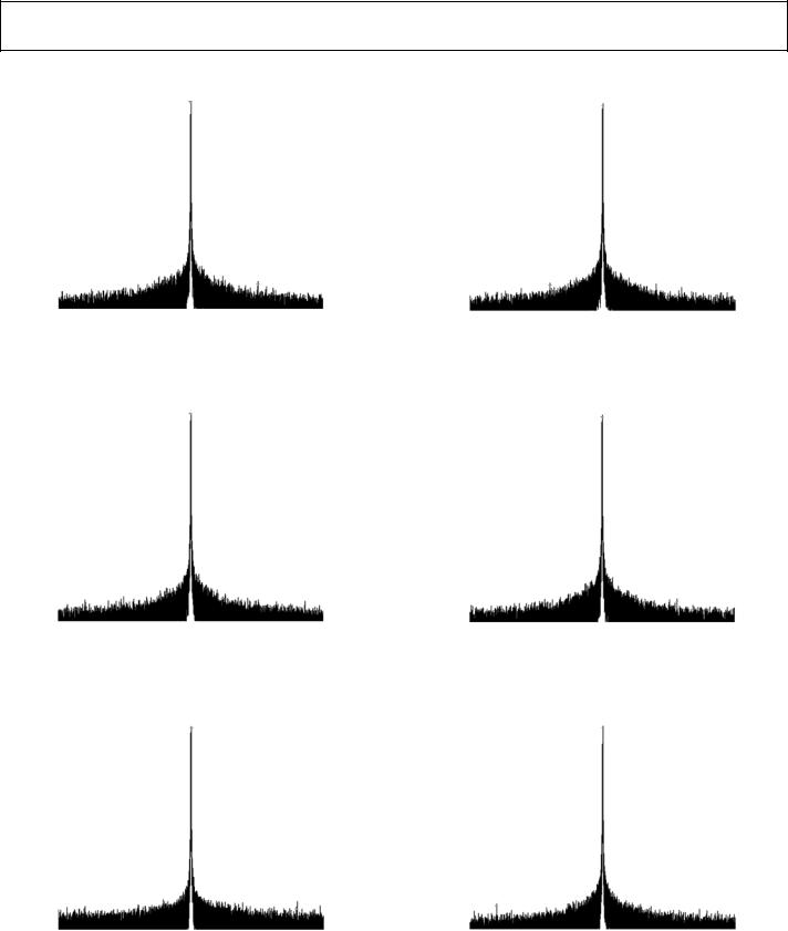
Figure 8. Wideband SFDR, fOUT = 75.1 MHz, fCLK = 500 MSPS |
|
|
||||||||||||||||
|
|
|
REF LVL |
DELTA 1 (T1) |
RBW |
20kHz |
RF ATT |
20dB |
|
|
|||||||||
|
|
|
0dBm |
–53.84dB |
VBW |
20kHz |
|
|
|
|
|
|
|||||||
|
0 |
|
|
|
|
|
–101.20240481MHz |
SWT |
1.6s |
UNIT |
dB |
|
|
||||||
|
|
|
|
|
|
|
|
|
|
|
|
|
|
|
|
|
|
|
|
|
|
|
|
|
|
|
|
|
|
|
|
|
|
1 |
|
|
|
|
|
|
–10 |
|
|
|
|
|
|
|
|
|
|
|
|
|
|
|
|
||
|
|
|
|
|
|
|
|
|
|
|
|
|
|
|
|
|
|||
|
|
|
|
|
|
|
|
|
|
|
|
|
|
|
|
|
|
||
|
–20 |
|
|
|
|
|
|
|
|
|
|
|
|
|
1AP |
||||
|
|
|
|
|
|
|
|
|
|
|
|
|
|
|
|
||||
|
|
|
|
|
|
|
|
|
|
|
|
|
|
|
|
|
|
||
|
–30 |
|
|
|
|
|
|
|
|
|
|
|
|
|
|
|
|||
|
|
|
|
|
|
|
|
|
|
|
|
|
|
|
|
|
|
||
(dB) |
–40 |
|
|
|
|
|
|
|
|
|
|
|
|
|
|
|
|||
|
|
|
|
|
|
|
|
|
|
|
|
|
|
|
|
|
|||
–50 |
|
|
|
|
|
|
|
|
|
|
|
|
|
|
|
|
|
||
|
|
|
|
|
|
|
|
|
|
|
|
|
|
|
|
|
|
||
|
–60 |
|
|
|
|
|
|
|
|
|
|
|
|
|
|
|
|||
|
|
|
|
|
|
|
|
|
|
|
|
|
|
|
|
|
|
||
|
–70 |
|
|
|
|
|
|
|
|
|
|
|
|
|
|
|
|||
|
|
|
|
|
|
|
|
|
|
|
|
|
|
|
|
|
|
||
|
–80 |
|
|
|
|
|
|
|
|
|
|
|
|
|
|
|
|||
|
|
|
|
|
|
|
|
|
|
|
|
|
|
|
|
|
|
||
|
–90 |
|
|
|
|
|
|
|
|
|
|
|
|
|
-011 |
||||
|
|
|
|
|
|
|
|
|
|
|
|
|
|
|
|
||||
|
–100 |
|
|
|
|
|
|
|
|
|
|
|
|
|
|
|
|||
|
|
|
|
|
|
|
|
|
|
|
|
|
|
05252 |
|||||
|
|
|
|
|
|
|
|
|
|
|
|
|
|||||||
|
START 0Hz |
|
|
25MHz/DIV |
|
|
STOP 250MHz |
||||||||||||
Figure 9. Wideband SFDR, fOUT = 200.3 MHz, fCLK = 500 MSPS
Rev. A | Page 11 of 44
AD9958
|
|
REF LVL |
DELTA 1 (T1) |
RBW |
500Hz |
RF ATT |
20dB |
|
||||||||
|
|
0dBm |
–84.73dB |
|
VBW |
500Hz |
|
|
|
|
|
|
|
|||
|
0 |
|
|
254.50901604kHz |
SWT |
20s |
UNIT |
dB |
|
|||||||
|
|
|
|
|
|
1 |
|
|
|
|
|
|
|
|
|
|
|
–10 |
|
|
|
|
|
|
|
|
|
|
|
|
|
|
|
|
|
|
|
|
|
|
|
|
|
|
|
|
|
|
|
|
|
|
|
|
|
|
|
|
|
|
|
|
|
|
|
|
|
|
–20 |
|
|
|
|
|
|
|
|
|
|
|
1AP |
|
||
|
|
|
|
|
|
|
|
|
|
|
|
|
||||
|
|
|
|
|
|
|
|
|
|
|
|
|
|
|||
|
–30 |
|
|
|
|
|
|
|
|
|
|
|
|
|
|
|
|
|
|
|
|
|
|
|
|
|
|
|
|
|
|
|
|
(dB) |
–40 |
|
|
|
|
|
|
|
|
|
|
|
|
|
|
|
|
|
|
|
|
|
|
|
|
|
|
|
|
|
|
||
–50 |
|
|
|
|
|
|
|
|
|
|
|
|
|
|
|
|
|
|
|
|
|
|
|
|
|
|
|
|
|
|
|
|
|
|
–60 |
|
|
|
|
|
|
|
|
|
|
|
|
|
|
|
|
|
|
|
|
|
|
|
|
|
|
|
|
|
|
|
|
|
|
|
|
|
|
|
|
|
|
|
|
|
|
|
|
|
|
–70 |
|
|
|
|
|
|
|
|
|
|
|
|
|
|
|
|
|
|
|
|
|
|
|
|
|
|
|
|
|
|
|
|
|
–80 |
|
|
|
|
|
|
|
|
|
|
|
|
|
|
|
|
|
|
|
|
|
|
|
|
|
|
|
|
|
|
|
|
|
–90 |
|
|
|
|
|
|
|
|
|
|
|
|
|
|
-012 |
|
|
|
|
|
|
|
|
|
|
|
|
|
|
|
||
|
–100 |
|
|
|
|
|
|
|
|
|
|
|
|
|
|
|
|
|
|
|
|
|
|
|
|
|
|
|
|
|
|
05252 |
|
|
|
|
|
|
|
|
|
|
|
|
|
|
|
|
||
|
CENTER 1.1MHz |
100kHz/DIV |
|
|
|
SPAN 1MHz |
||||||||||
|
Figure 10. NBSFDR, fOUT = 1.1 MHz, fCLK = 500 MSPS, ±1 MHz |
|
||||||||||||||
|
|
REF LVL |
DELTA 1 (T1) |
RBW |
500Hz |
RF ATT |
20dB |
|
||||||||
|
|
0dBm |
–84.10dB |
|
VBW |
500Hz |
|
|
|
|
|
|
|
|||
|
0 |
|
|
120.24048096kHz |
SWT |
20s |
UNIT |
dB |
|
|||||||
|
|
|
|
|
|
|
|
|
|
|
|
|
|
|
|
|
|
|
|
|
|
|
1 |
|
|
|
|
|
|
|
|
|
|
|
–10 |
|
|
|
|
|
|
|
|
|
|
|
|
|
|
|
|
|
|
|
|
|
|
|
|
|
|
|
|
|
|
|
|
|
–20 |
|
|
|
|
|
|
|
|
|
|
|
1AP |
|
||
|
|
|
|
|
|
|
|
|
|
|
|
|
||||
|
|
|
|
|
|
|
|
|
|
|
|
|
|
|||
|
–30 |
|
|
|
|
|
|
|
|
|
|
|
|
|
|
|
|
|
|
|
|
|
|
|
|
|
|
|
|
|
|
|
|
(dB) |
–40 |
|
|
|
|
|
|
|
|
|
|
|
|
|
|
|
|
|
|
|
|
|
|
|
|
|
|
|
|
|
|
||
–50 |
|
|
|
|
|
|
|
|
|
|
|
|
|
|
|
|
|
|
|
|
|
|
|
|
|
|
|
|
|
|
|
|
|
|
–60 |
|
|
|
|
|
|
|
|
|
|
|
|
|
|
|
|
|
|
|
|
|
|
|
|
|
|
|
|
|
|
|
|
|
–70 |
|
|
|
|
|
|
|
|
|
|
|
|
|
|
|
|
|
|
|
|
|
|
|
|
|
|
|
|
|
|
|
|
|
–80 |
|
|
|
|
|
|
|
|
|
|
|
|
|
|
|
|
|
|
|
|
|
|
|
|
|
|
|
|
|
|
|
|
|
|
|
|
|
|
|
|
|
|
|
|
|
|
|
|
|
|
–90 |
|
|
|
|
|
|
|
|
|
|
|
|
|
|
-013 |
|
|
|
|
|
|
|
|
|
|
|
|
|
|
|
||
|
–100 |
|
|
|
|
|
|
|
|
|
|
|
|
|
|
|
|
|
|
|
|
|
|
|
|
|
|
|
|
|
|
05252 |
|
|
|
|
|
|
|
|
|
|
|
|
|
|
|
|||
|
CENTER 40.1MHz |
100kHz/DIV |
|
|
|
SPAN 1MHz |
||||||||||
|
Figure 11. NBSFDR, fOUT = 40.1 MHz, fCLK = 500 MSPS, ±1 MHz |
|
||||||||||||||
|
|
REF LVL |
DELTA 1 (T1) |
RBW |
500Hz |
RF ATT |
20dB |
|
||||||||
|
|
0dBm |
–82.63dB |
|
VBW |
500Hz |
|
|
|
|
|
|
|
|||
|
0 |
|
|
400.80160321kHz |
SWT |
20s |
UNIT |
dB |
|
|||||||
|
|
|
|
|
|
1 |
|
|
|
|
|
|
|
|
|
|
|
–10 |
|
|
|
|
|
|
|
|
|
|
|
|
|
|
|
|
|
|
|
|
|
|
|
|
|
|
|
|
|
|
|
|
|
|
|
|
|
|
|
|
|
|
|
|
|
|
|
|
|
|
–20 |
|
|
|
|
|
|
|
|
|
|
|
|
1AP |
|
|
|
|
|
|
|
|
|
|
|
|
|
|
|
|
|||
|
|
|
|
|
|
|
|
|
|
|
|
|
|
|
||
|
–30 |
|
|
|
|
|
|
|
|
|
|
|
|
|
|
|
|
|
|
|
|
|
|
|
|
|
|
|
|
|
|
|
|
(dB) |
–40 |
|
|
|
|
|
|
|
|
|
|
|
|
|
|
|
|
|
|
|
|
|
|
|
|
|
|
|
|
|
|
||
–50 |
|
|
|
|
|
|
|
|
|
|
|
|
|
|
|
|
|
|
|
|
|
|
|
|
|
|
|
|
|
|
|
|
|
|
–60 |
|
|
|
|
|
|
|
|
|
|
|
|
|
|
|
|
|
|
|
|
|
|
|
|
|
|
|
|
|
|
|
|
|
–70 |
|
|
|
|
|
|
|
|
|
|
|
|
|
|
|
|
|
|
|
|
|
|
|
|
|
|
|
|
|
|
|
|
|
–80 |
|
|
|
|
|
|
|
|
|
|
|
|
|
|
|
|
|
|
|
|
|
|
|
|
|
|
|
|
|
|
|
|
|
–90 |
|
|
|
|
|
|
|
|
|
|
|
|
|
|
-014 |
|
|
|
|
|
|
|
|
|
|
|
|
|
|
|
||
|
–100 |
|
|
|
|
|
|
|
|
|
|
|
|
|
|
|
|
|
|
|
|
|
|
|
|
|
|
|
|
|
|
05252 |
|
|
|
|
|
|
|
|
|
|
|
|
|
|
|
|||
|
CENTER 100.3MHz |
100kHz/DIV |
|
|
|
SPAN 1MHz |
||||||||||
Figure 12. NBSFDR, fOUT = 100.3 MHz, fCLK = 500 MSPS, ±1 MHz
|
|
REF LVL |
DELTA 1 (T1) |
RBW |
500Hz |
RF ATT |
20dB |
|||||||
|
|
0dBm |
–84.86dB |
|
VBW |
500Hz |
|
|
|
|
|
|||
|
0 |
|
|
–200.40080160kHz |
SWT |
20s |
UNIT |
dB |
||||||
|
|
|
|
|
|
|
|
|
|
|
|
|
|
|
|
|
|
|
|
|
1 |
|
|
|
|
|
|
|
|
|
–10 |
|
|
|
|
|
|
|
|
|
|
|
|
|
|
|
|
|
|
|
|
|
|
|
|
|
|
|
|
|
–20 |
|
|
|
|
|
|
|
|
|
|
|
1AP |
|
|
|
|
|
|
|
|
|
|
|
|
|
|||
|
|
|
|
|
|
|
|
|
|
|
|
|
||
|
–30 |
|
|
|
|
|
|
|
|
|
|
|
|
|
|
|
|
|
|
|
|
|
|
|
|
|
|
|
|
(dB) |
–40 |
|
|
|
|
|
|
|
|
|
|
|
|
|
|
|
|
|
|
|
|
|
|
|
|
|
|
||
–50 |
|
|
|
|
|
|
|
|
|
|
|
|
|
|
|
|
|
|
|
|
|
|
|
|
|
|
|
|
|
|
–60 |
|
|
|
|
|
|
|
|
|
|
|
|
|
|
|
|
|
|
|
|
|
|
|
|
|
|
|
|
|
–70 |
|
|
|
|
|
|
|
|
|
|
|
|
|
|
|
|
|
|
|
|
|
|
|
|
|
|
|
|
|
–80 |
|
|
|
|
|
|
|
|
|
|
|
|
|
|
|
|
|
|
|
|
|
|
|
|
|
|
|
|
|
–90 |
|
|
|
|
|
|
|
|
|
|
|
|
|
|
|
|
|
|
|
|
|
|
|
|
|
|
|
|
|
–100 |
|
|
|
|
|
|
|
|
|
|
|
|
|
|
|
|
|
|
100kHz/DIV |
|
|
|
SPAN 1MHz |
|||||
|
CENTER 15.1MHz |
|
|
|
||||||||||
|
Figure 13. NBSFDR, fOUT = 15.1 MHz, fCLK = 500 MSPS, ±1 MHz |
|||||||||||||
|
|
REF LVL |
DELTA 1 (T1) |
RBW |
500Hz |
RF ATT |
20dB |
|||||||
|
|
0dBm |
–86.03dB |
|
VBW |
500Hz |
|
|
|
|
|
|||
|
0 |
|
|
262.56513026kHz |
SWT |
20s |
UNIT |
dB |
||||||
|
|
|
|
|
|
|
|
|
|
|
|
|
|
|
|
|
|
|
|
|
1 |
|
|
|
|
|
|
|
|
|
–10 |
|
|
|
|
|
|
|
|
|
|
|
|
|
|
|
|
|
|
|
|
|
|
|
|
|
|
||
|
|
|
|
|
|
|
|
|
|
|
|
|
|
|
|
|
|
|
|
|
|
|
|
|
|
|
|
|
|
|
–20 |
|
|
|
|
|
|
|
|
|
|
|
1AP |
|
|
|
|
|
|
|
|
|
|
|
|
|
|||
|
|
|
|
|
|
|
|
|
|
|
|
|
||
|
–30 |
|
|
|
|
|
|
|
|
|
|
|
|
|
|
|
|
|
|
|
|
|
|
|
|
|
|
|
|
(dB) |
–40 |
|
|
|
|
|
|
|
|
|
|
|
|
|
|
|
|
|
|
|
|
|
|
|
|
|
|
||
–50 |
|
|
|
|
|
|
|
|
|
|
|
|
|
|
|
|
|
|
|
|
|
|
|
|
|
|
|
|
|
|
–60 |
|
|
|
|
|
|
|
|
|
|
|
|
|
|
|
|
|
|
|
|
|
|
|
|
|
|
|
|
|
–70 |
|
|
|
|
|
|
|
|
|
|
|
|
|
|
|
|
|
|
|
|
|
|
|
|
|
|
|
|
|
|
|
|
|
|
|
|
|
|
|
|
|
|
|
|
–80 |
|
|
|
|
|
|
|
|
|
|
|
|
|
|
|
|
|
|
|
|
|
|
|
|
|
|
|
|
|
–90 |
|
|
|
|
|
|
|
|
|
|
|
|
|
|
|
|
|
|
|
|
|
|
|
|
|
|
|
|
|
–100 |
|
|
|
|
|
|
|
|
|
|
|
|
|
|
|
|
|
100kHz/DIV |
|
|
|
SPAN 1MHz |
||||||
|
CENTER 75.1MHz |
|
|
|
||||||||||
|
Figure 14. NBSFDR, fOUT = 75.1 MHz, fCLK = 500 MSPS, ±1 MHz |
|||||||||||||
|
|
REF LVL |
DELTA 1 (T1) |
|
RBW |
500Hz |
RF ATT |
20dB |
||||||
|
|
0dBm |
–83.72dB |
|
VBW |
500Hz |
|
|
|
|
|
|||
|
0 |
|
|
–400.80160321kHz |
SWT |
20s |
UNIT |
dB |
||||||
|
|
|
|
|
|
|
|
|
|
|
|
|
|
|
|
|
|
|
|
|
1 |
|
|
|
|
|
|
|
|
|
–10 |
|
|
|
|
|
|
|
|
|
|
|
|
|
|
|
|
|
|
|
|
|
|
|
|
|
|
||
|
|
|
|
|
|
|
|
|
|
|
|
|
|
|
|
|
|
|
|
|
|
|
|
|
|
|
|
|
|
|
–20 |
|
|
|
|
|
|
|
|
|
|
|
1AP |
|
|
|
|
|
|
|
|
|
|
|
|
|
|||
|
|
|
|
|
|
|
|
|
|
|
|
|
||
|
–30 |
|
|
|
|
|
|
|
|
|
|
|
|
|
|
|
|
|
|
|
|
|
|
|
|
|
|
|
|
(dB) |
–40 |
|
|
|
|
|
|
|
|
|
|
|
|
|
|
|
|
|
|
|
|
|
|
|
|
|
|
||
–50 |
|
|
|
|
|
|
|
|
|
|
|
|
|
|
|
|
|
|
|
|
|
|
|
|
|
|
|
|
|
|
–60 |
|
|
|
|
|
|
|
|
|
|
|
|
|
|
|
|
|
|
|
|
|
|
|
|
|
|
|
|
|
|
|
|
|
|
|
|
|
|
|
|
|
|
|
|
–70 |
|
|
|
|
|
|
|
|
|
|
|
|
|
|
|
|
|
|
|
|
|
|
|
|
|
|
|
|
|
–80 |
|
|
|
|
|
|
|
|
|
|
|
|
|
|
|
|
|
|
|
|
|
|
|
|
|
|
|
|
|
–90 |
|
|
|
|
|
|
|
|
|
|
|
|
|
|
|
|
|
|
|
|
|
|
|
|
|
|
|
|
|
–100 |
|
|
|
|
|
|
|
|
|
|
|
|
|
|
|
|
|
100kHz/DIV |
|
|
|
SPAN 1MHz |
||||||
|
CENTER 200.3MHz |
|
|
|
||||||||||
Figure 15. NBSFDR fOUT = 200. 3MHz, fCLK = 500 MSPS, , ±1 MHz
05252-015
05252-016
05252-017
Rev. A | Page 12 of 44

AD9958
|
–100 |
|
|
|
|
|
|
|
–110 |
75.1MHz |
|
|
|
|
|
(dBc/Hz) |
–120 |
|
|
|
|
|
|
–130 |
|
|
|
|
|
|
|
NOISE |
|
|
100.3MHz |
|
|
||
|
|
|
|
|
|||
–140 |
|
|
|
|
|
|
|
PHASE |
|
|
|
|
|
|
|
–150 |
40.1MHz |
|
|
|
|
|
|
|
|
|
|
|
|
|
|
|
–160 |
|
|
|
|
|
|
|
|
|
15.1MHz |
|
|
|
|
|
–170 |
100 |
1k |
10k |
100k |
1M |
10M |
|
10 |
||||||
|
|
|
FREQUENCY OFFSET (Hz) |
|
05252018- |
||
Figure 16. Residual Phase Noise (SSB) with fOUT = 15.1 MHz, 40.1MHz, 75.1 MHz, 100.3 MHz; fCLK = 500 MHz with REFCLK Multiplier Bypassed
|
–70 |
|
|
|
|
|
|
|
|
–80 |
|
|
|
|
|
|
|
|
–90 |
|
|
|
|
|
|
|
(dBc/Hz) |
–100 |
|
100.3MHz |
|
|
|
|
|
|
|
|
|
|
|
|
||
–110 |
|
|
75.1MHz |
|
|
|
|
|
NOISE |
–120 |
|
|
|
|
|
|
|
|
|
|
|
|
|
|
||
–130 |
|
|
|
|
|
|
|
|
PHASE |
|
|
|
|
|
|
|
|
–140 |
40.1MHz |
|
|
|
|
|
||
|
|
|
|
|
|
|
||
|
–150 |
|
15.1MHz |
|
|
|
|
|
|
|
|
|
|
|
|
|
|
|
–160 |
|
|
|
|
|
|
|
|
–170 |
|
|
|
|
|
|
-019 |
|
10 |
100 |
1k |
10k |
100k |
1M |
10M |
|
|
|
|
FREQUENCY OFFSET (Hz) |
|
|
05252 |
||
Figure 17. Residual Phase Noise (SSB) with fOUT = 15.1 MHz, 40.1MHz, 75.1 MHz, 100.3 MHz; fCLK = 500 MHz with REFCLK Multiplier = 5×
|
–70 |
|
|
|
|
|
|
|
–80 |
|
|
|
|
|
|
|
–90 |
|
|
|
|
|
|
(dBc/Hz) |
–100 |
|
|
100.3MHz |
|
|
|
–110 |
|
|
75.1MHz |
|
|
||
NOISE |
–120 |
|
|
|
|
|
|
–130 |
|
|
|
|
|
|
|
PHASE |
|
40.1MHz |
|
|
|
|
|
|
|
|
|
|
|
||
–140 |
|
15.1MHz |
|
|
|
||
|
|
|
|
|
|
||
|
–150 |
|
|
|
|
|
|
|
–160 |
|
|
|
|
|
|
|
–170 |
100 |
1k |
10k |
100k |
1M |
10M |
|
10 |
||||||
|
|
|
FREQUENCY OFFSET (Hz) |
|
05252020- |
||
Figure 18. Residual Phase Noise (SSB) with fOUT = 15.1 MHz, 40.1MHz, 75.1 MHz,100.3 MHz; fCLK = 500 MHz with REFCLK Multiplier = 20×
|
–60 |
|
|
|
|
|
|
|
(dBc) |
–65 |
|
|
|
|
|
|
|
|
|
|
|
|
|
|
|
|
ISOLATION |
–70 |
SINGLE DAC POWER PLANE |
|
|
|
|||
|
|
|
|
|||||
CHANNEL |
|
|
|
|
||||
–75 |
|
|
|
|
|
|
|
|
|
|
|
|
|
|
|
|
|
|
–80 |
|
|
|
|
|
|
|
|
|
|
SEPARATED DAC POWER PLANES |
|
||||
|
–85 |
50.3 |
75.3 |
100.3 |
125.3 |
150.3 |
175.3 |
200.3 |
|
25.3 |
|||||||
|
|
FREQUENCY OF COUPLING SPUR (MHz) |
05252021- |
|||||
Figure 19. Channel Isolation at 500 MSPS Operation; Conditions are Channel of Interest Fixed at 110.3 MHz, the Other Channels Are Frequency Swept
|
600 |
|
|
|
|
(mW) |
500 |
|
|
|
|
|
|
|
|
|
|
DISSIPATION |
400 |
|
|
|
|
2 CHANNELS ON |
|
|
|
|
|
300 |
|
|
|
|
|
POWER |
1 CHANNEL ON |
|
|
|
|
200 |
|
|
|
|
|
TOTAL |
100 |
|
|
|
|
|
0 |
|
|
|
-022 |
|
500 450 400 350 300 250 200 |
150 |
100 |
50 |
|
|
REFERENCE CLOCK FREQUENCY (MHz) |
|
|
05252 |
|
Figure 20. Power Dissipation vs. Reference Clock Frequency vs. Channel(s) Power On/Off
|
–45 |
|
|
|
|
|
|
–50 |
|
|
|
|
|
|
–55 |
|
|
SFDR AVERAGED |
|
|
|
|
|
|
|
|
|
(dBc) |
–60 |
|
|
|
|
|
SFDR |
|
|
|
|
|
|
|
|
|
|
|
|
|
|
–65 |
|
|
|
|
|
|
–70 |
|
|
|
|
|
|
–75 |
15.1 |
40.1 |
75.1 |
100.3 |
200.3 |
|
1.1 |
|||||
|
|
|
fOUT (MHz) |
|
05252023- |
|
Figure 21. Averaged Channel SFDR vs. fOUT
Rev. A | Page 13 of 44
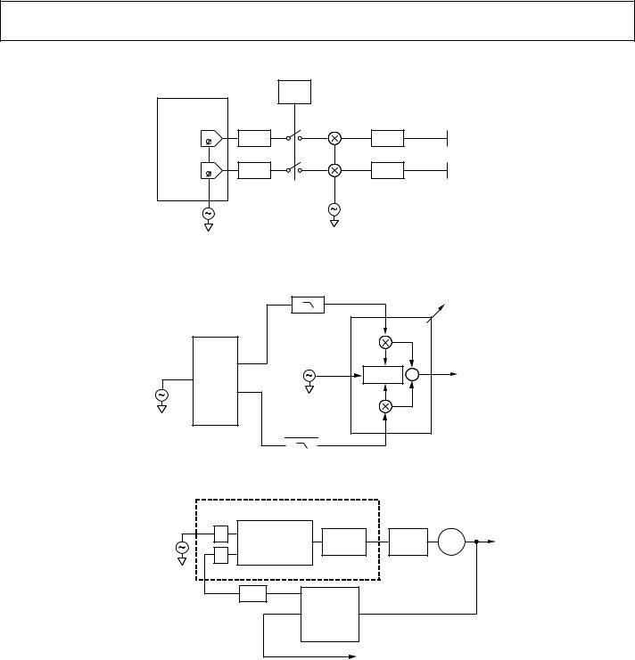
AD9958
APPLICATION CIRCUITS
|
|
PULSE |
AD9958 |
|
ANTENNA |
|
RADIATING |
|
|
|
ELEMENTS |
CH0 |
FILTER |
FILTER |
CH1 |
FILTER |
FILTER |
REFCLK |
|
LO |
|
|
05252-024
Figure 22. Phase Array Radar Using Precision Frequency/Phase Control from DDS in FMCW or Pulsed Radar Applications; DDS Provides Either Continuous Wave or Frequency Sweep
|
|
|
AD8348 |
|
I BASEBAND |
AD8347 |
|
|
|
|
AD8346 |
|
|
|
ADL5390 |
|
|
AD8349 |
|
|
CH0 |
|
|
|
LO |
PHASE |
RF OUTPUT |
AD9958 |
|
SPLITTER |
|
CH1 |
|
||
|
|
||
REFCLK |
|
|
|

 Q BASEBAND
Figure 23. Single-Sideband-Suppressed Carrier Upconversion
AD9510, AD9511, ADF4106
05252-025
|
÷ |
PHASE |
CHARGE |
LOOP |
VCO |
REFERENCE |
|
COMPARATOR |
PUMP |
FILTER |
|
÷ |
|
||||
|
|
|
|
|
LPF
AD9958 REFCLK
05252-026
Figure 24. DDS in PLL Locking to Reference Offering Distribution with Fine Frequency and Delay Adjust Tuning
Rev. A | Page 14 of 44
Loading...