


 Loading...
Analog Devices AD843JR-16, AD843JN, AD843JCHIPS, AD843BQ, AD843BH Datasheet
...a |
34 MHz, CBFET |
|
Fast Settling Op Amp |
||
|
|
|
|
|
AD843 |
|
|
|
FEATURES
AC PERFORMANCE
Unity Gain Bandwidth: 34 MHz
Fast Settling: 135 ns to 0.01%
Slew Rate: 250 V/ms
Stable at Gains of 1 or Greater
Full Power Bandwidth: 3.9 MHz
DC PERFORMANCE
Input Offset Voltage: 1 mV max (AD843K/B} Input Bias Current: 0.6 nA typ
Input Voltage Noise: 19 nV/ÖHz
Open Loop Gain: 30 V/mV into a 500 V Load
Output Current: 50 mA min Supply Current: 13 mA max
Available in 8-Pin Plastic Mini-DIP & Cerdip, 16-Pin SOIC, 20-Pin LCC and 12-Pin Hermetic Metal Can Packages
Available in Tape and Reel in Accordance with EIA-481A Standard
Chips and MIL-STD-883B Parts Also Available
APPLICATIONS
High Speed Sample-and-Hold Amplifiers
High Bandwidth Active Filters
High Speed Integrators
High Frequency Signal Conditioning
PRODUCT DESCRIPTION
The AD843 is a fast settling, 34 MHz, CBFET input op amp. The AD843 combines the low (0.6 nA) input bias currents characteristic of a FET input amplifier while still providing a 34 MHz bandwidth and a 135 ns settling time (to within 0.01% of final value for a 10 volt step). The AD843 is a member of the Analog Devices’ family of wide bandwidth operational amplifiers. These devices are fabricated using Analog Devices’ junction isolated complementary bipolar (CB) process. This process permits a combination of dc precision and wideband ac performance previously unobtainable in a monolithic op amp.
The 250 V/μs slew rate and 0.6 nA input bias current of the AD843 ensure excellent performance in high speed sample-and- hold applications and in high speed integrators. This amplifier is also ideally suited for high bandwidth active filters and high frequency signal conditioning circuits.
Unlike many high frequency amplifiers, the AD843 requires no external compensation and it remains stable over its full operating temperature range. It is available in five performance grades: the AD843J and AD843K are rated over the commercial temperature range of 0°C to +70°C. The AD843A and AD843B are rated over the industrial temperature range of –40°C to +85°C. The AD843S is rated over the military temperature range of –55°C to +125°C and is available processed to MIL-STD-883B, Rev. C.
REV. D
Information furnished by Analog Devices is believed to be accurate and reliable. However, no responsibility is assumed by Analog Devices for its use, nor for any infringements of patents or other rights of third parties which may result from its use. No license is granted by implication or otherwise under any patent or patent rights of Analog Devices.
CONNECTION DIAGRAMS
16-Pin SOIC (R-16) Package |
Plastic (N-8) and |
|
Cerdip (Q-8) Package |
TO-8 (H-12A) Package |
LCC (E-20A) Package |
The AD843 is offered in either 8-pin plastic DIP or hermetic cerdip packages, in 16-pin SOIC, 20-Pin LCC, or in a 12-pin metal can. Chips are also available.
PRODUCT HIGHLIGHTS
1.The high slew rate, fast settling time and low input bias current of the AD843 make it the ideal amplifier for 12-bit D/A and A/D buffers, for high speed sample-and-hold amplifiers and for high speed integrator circuits. The AD843 can replace many FET input hybrid amplifiers such as the LH0032, LH4104 and OPA600.
2.Fully differential inputs provide outstanding performance in all standard high frequency op amp applications such as signal conditioning and active filters.
3.Laser wafer trimming reduces the input offset voltage to
1mV max (AD843K and AD843B).
4.Although external offset nulling is unnecessary in many applications, offset null pins are provided.
5.The AD843 does not require external compensation at closed loop gains of 1 or greater.
©Analog Devices, Inc., 1995
One Technology Way, P.O. Box 9106, Norwood. MA 02062-9106, U.S.A. Tel: 617/329-4700 Fax: 617/326-8703

AD843–SPECIFICATIONS (@ TA = +25°C and ±15 V dc, unless otherwise noted)
|
|
|
|
AD843J/A |
|
|
AD843K/B |
|
|
AD843S1 |
|
|
|
|
Model |
Conditions |
Min |
Typ |
Max |
Min |
Typ |
Max |
Min |
Typ |
Max |
Units |
|||
|
|
|
|
|
|
|
|
|
|
|
|
|
|
|
INPUT OFFSET VOLTAGE1 |
|
|
|
1.0 |
2.0 |
|
0.5 |
1.0 |
|
1.0 |
2.0 |
mV |
||
|
TMIN-TMAX |
|
1.7 |
4.0 |
|
1.2 |
2.0 |
|
3.0 |
4.5 |
mV |
|||
Offset Drift |
|
|
|
12 |
|
|
12 |
35 |
|
12 |
|
mV/°C |
||
|
|
|
|
|
|
|
|
|
|
|
|
|
|
|
INPUT BIAS CURRENT |
Initial (TJ = +25°C) |
|
50 |
|
|
40 |
|
|
50 |
|
pA |
|||
|
Warmed-Up2 |
|
0.8 |
2.5 |
|
0.6 |
1.0 |
|
0.8 |
2.5 |
nA |
|||
|
TMIN-TMAX |
|
|
60/160 |
|
|
23/65 |
|
|
2600 |
nA |
|||
INPUT OFFSET CURRENT |
Initial (TJ = +25°C) |
|
30 |
|
|
20 |
|
|
30 |
|
pA |
|||
|
Warmed-Up2 |
|
0.25 |
1.0 |
|
0.2 |
0.4 |
|
0.25 |
1.0 |
nA |
|||
|
TMIN-TMAX |
|
|
23/64 |
|
|
9/26 |
|
|
1025 |
nA |
|||
INPUT CHARACTERISTICS |
|
|
|
1010 |
|
|
1010 |
|
|
1010 |
|
W |
||
Input Resistance |
|
|
|
|
|
|
|
|
||||||
Input Capacitance |
|
|
|
6 |
|
|
6 |
|
|
6 |
|
pF |
||
|
|
|
|
|
|
|
|
|
|
|
|
|
|
|
INPUT VOLTAGE RANGE |
|
|
610 |
|
|
610 |
|
|
610 |
|
|
|
|
|
Common Mode |
|
|
+12, |
|
+12, |
|
+12, |
|
V |
|||||
|
|
|
|
–13 |
|
|
–13 |
|
|
–13 |
|
|
|
|
|
|
|
|
|
|
|
|
|
|
|
|
|
|
|
COMMON-MODE REJECTION |
VCM = ±10 V |
60 |
72 |
|
70 |
76 |
|
60 |
72 |
|
dB |
|||
|
TMIN-TMAX |
60 |
72 |
|
68 |
76 |
|
60 |
72 |
|
dB |
|||
INPUT VOLTAGE NOISE |
f = 10 kHz |
|
19 |
|
|
19 |
|
|
19 |
|
nV/Ö |
|
|
|
|
|
|
|
|
|
Hz |
||||||||
Wideband Noise |
10 Hz to 10 MHz |
|
60 |
|
|
60 |
|
|
60 |
|
mV rms |
|||
|
|
|
|
|
|
|
|
|
|
|
|
|
|
|
OPEN LOOP GAIN |
VO = ±10 V |
|
|
|
|
|
|
|
|
|
|
|
|
|
|
RLOAD ³ 500 W |
15 |
25 |
|
20 |
30 |
|
15 |
30 |
|
V/mV |
|||
|
TMIN-TMAX |
10 |
20 |
|
10 |
25 |
|
10 |
25 |
|
V/mV |
|||
OUTPUT CHARACTERISTICS |
RLOAD ³ 500 W |
610 |
|
|
610 |
|
|
610 |
|
|
|
|
|
|
Voltage |
+11.5, |
|
+11.5, |
|
+11.5, |
|
V |
|||||||
|
VOUT = ±10 V |
50 |
–12.6 |
|
50 |
–12.6 |
|
50 |
–12.6 |
|
|
|
|
|
Current |
|
|
|
|
|
|
mA |
|||||||
Output Resistance |
Open Loop |
|
12 |
|
|
12 |
|
|
12 |
|
W |
|||
|
|
|
|
|
|
|
|
|
|
|
|
|
|
|
FREQUENCY RESPONSE |
|
|
|
|
|
|
|
|
|
|
|
|
|
|
Unity Gain Bandwidth |
VOUT = 90 mV p-p |
|
34 |
|
|
34 |
|
|
34 |
|
MHz |
|||
Full Power Bandwidth3 |
VO |
= 20 V p-p |
|
|
|
|
|
|
|
|
|
|
|
|
|
R1 |
³ 500 W |
2.5 |
3.9 |
|
2.5 |
3.9 |
|
2.5 |
3.9 |
|
MHz |
||
Rise Time |
AVCL = –1 |
|
10 |
|
|
10 |
|
|
10 |
|
ns |
|||
Overshoot |
AVCL = –1 |
|
15 |
|
|
15 |
|
|
15 |
|
% |
|
|
|
Slew Rate |
AVCL = –1 |
160 |
250 |
|
160 |
250 |
|
160 |
250 |
|
V/ms |
|||
Settling Time |
10 V Step |
|
|
|
|
|
|
|
|
|
|
|
|
|
|
AVCL = –1 |
|
|
|
|
|
|
|
|
|
|
|
|
|
|
to 0.1% |
|
95 |
|
|
95 |
|
|
95 |
|
ns |
|||
|
to 0.01% |
|
135 |
|
|
135 |
|
|
135 |
|
ns |
|||
Overdrive Recovery |
–Overdrive |
|
200 |
|
|
200 |
|
|
200 |
|
ns |
|||
|
+Overdrive |
|
700 |
|
|
700 |
|
|
700 |
|
ns |
|||
Differential Gain |
f = 4.4 MHz |
|
0.025 |
|
|
0.025 |
|
|
0.025 |
|
% |
|
|
|
Differential Phase |
f = 4.4 MHz |
|
0.025 |
|
|
0.025 |
|
|
0.025 |
|
Degree |
|||
|
|
|
|
|
|
|
|
|
|
|
|
|
|
|
POWER SUPPLY |
|
|
|
± 15 |
|
|
±15 |
|
|
±15 |
|
|
|
|
Rated Performance |
|
|
64.5 |
618 |
64.5 |
618 |
64.5 |
618 |
V |
|||||
Operating Range |
|
|
|
|
|
V |
||||||||
Quiescent Current |
|
|
|
12 |
13 |
|
12 |
13 |
|
12 |
13 |
mA |
||
|
TMIN-TMAX |
|
12.3 |
14 |
|
12.3 |
14 |
|
12.5 |
16 |
mA |
|||
Rejection Ratio |
±5 V to ±18 V |
65 |
76 |
|
70 |
80 |
|
65 |
76 |
|
dB |
|||
Rejection Ratio |
TMIN-TMAX |
62 |
76 |
|
68 |
80 |
|
62 |
76 |
|
dB |
|||
TEMPERATURE RANGE |
|
|
|
|
|
|
|
|
|
|
|
|
|
|
Operating, Rated Performance |
|
|
|
|
|
|
|
|
|
|
|
|
|
|
Commercial (0°C to +70°C) |
|
|
AD843J |
|
|
AD843K |
|
|
|
|
|
|
|
|
Industrial (–40°C to +85°C) |
|
|
AD843A |
|
|
AD843B |
|
|
|
|
|
|
|
|
Military (–55°C to +125°C)4 |
|
|
|
|
|
|
|
|
|
AD843S |
|
|
|
|
PACKAGE OPTIONS |
|
|
|
|
|
|
|
|
|
|
|
|
|
|
Plastic (N-8) |
|
|
AD843JN |
|
AD843KN |
|
|
|
|
|
|
|
||
Cerdip (Q-8) |
|
|
AD843AQ |
|
AD843BQ |
|
AD843SQ, AD843SQ/883B |
|
|
|
||||
Metal Can (H-12A) |
|
|
|
|
|
AD843BH |
|
AD843SH, AD843SH/883B |
|
|
|
|||
LCC (E-20A) |
|
|
|
|
|
|
|
|
AD843SE/883B |
|
|
|
|
|
SOIC (R-16) |
|
|
AD843JR–16 |
|
|
|
|
|
|
|
|
|
|
|
Tape & Reel |
|
|
AD843JR-16–REEL |
|
|
|
|
|
|
|
|
|
||
|
|
|
AD843JR-16–REEL7 |
|
|
|
|
|
|
|
|
|
||
Chips |
|
|
AD843JCHIPS |
|
|
|
|
AD843SCHIPS |
|
|
|
|
||
|
|
|
|
|
|
|
|
|
|
|
|
|
|
|
–2– |
REV. D |
AD843
NOTES
1Standard Military Drawings Available: 5962-9098001M2A (SE/883B), 5962-9098001MXA (SH/883B), 5962-9098001MPA (SQ/883B). 2Specifications are guaranteed after 5 minutes at TA = +25°C.
3Full power bandwidth = Slew Rate/2 πV peak.
4All “S” grade TMIN-TMAX specifications are tested with automatic test equipment at TA = –55°C and TA = +125°C. Specifications subject to change without notice.
Specifications in boldface are tested on all production units at final electrical test. Results from those tests are used to calculate outgoing quality levels. All min and max specifications are guaranteed although only those shown in boldface are tested on all production units.
ABSOLUTE MAXIMUM RATINGS1 |
±18 V |
Supply Voltage . . . . . . . . . . . . . . . . . . . . . . . . |
|
Internal Power Dissipation2 |
|
Plastic Package . . . . . . . . . . . . . . . . . . . . . . |
. . . . 1.50 Watts |
Cerdip Package . . . . . . . . . . . . . . . . . . . . . |
. . . . 1.35 Watts |
12-Pin Header Package . . . . . . . . . . . . . . . |
. . . . 1.80 Watts |
16-Pin SOIC Package . . . . . . . . . . . . . . . . |
. . . . 1.50 Watts |
20-Pin LCC Package . . . . . . . . . . . . . . . . . |
. . . . . 1.00 Watt |
Input Voltage . . . . . . . . . . . . . . . . . . . . . . . . . |
. . . . . . . . . ±VS |
Output Short Circuit Duration . . . . . . . . . . . |
. . . . . Indefinite |
Differential Input Voltage . . . . . . . . . . . . . . . |
. . . +VS and –VS |
Storage Temperature Range (N, R) . . . . . . . |
–65°C to +125°C |
Storage Temperature Range (Q, H, E) . . . . –65°C to +150°C
Operating Temperature Range |
0°C to +70°C |
AD843J/R . . . . . . . . . . . . . . . . . . . . . . . . . |
|
AD843A/B . . . . . . . . . . . . . . . . . . . . . . . . . |
–40°C to +85°C |
AD843S . . . . . . . . . . . . . . . . . . . . . . . . . . |
–55°C to +125°C |
Lead Temperature Range (Soldering 60 sec) . |
. . . . . . . +300°C |
ESD Rating . . . . . . . . . . . . . . . . . . . . . . . . . . |
. . . . . . . . 500 V |
NOTES
1Stresses above those listed under “Absolute Maximum Ratings” may cause permanent damage to the device at these or any other conditions above those indicated in the operational sections of this specification is not implied. Exposure to absolute maximum rating conditions for extended periods may affect device
reliability.
28-Pin Plastic Package: θJA = 100°C/Watt 8-Pin Cerdip Package: θJA = 110°C/Watt 12-Pin Header Package: θJA = 80°C/Watt 16-Pin SOIC Package: θJA = 100°C/Watt 20-Pin LCC Package: θJA = 150°C/Watt
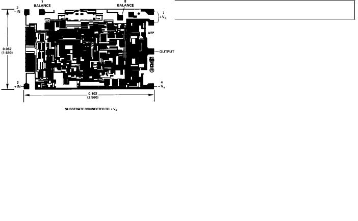
METALIZATION PHOTOGRAPH
Contact factory for latest dimensions. Dimensions shown in inches and (mm).
REV. D |
–3– |

AD843–Typical Characteristics
Figure 1. Input Voltage Range vs. Supply Voltage
Figure 2. Output Voltage Swing vs. Supply Voltage
Figure 3. Output Voltage Swing vs. Load Resistance
Figure 4. Quiescent Current vs. Supply Voltage
Figure 5. Input Bias Current vs. Junction Temperature
Figure 6. Output Impedance vs. Frequency
Figure 7. Input Bias Current vs. Common Mode Voltage
Figure 8. Short Circuit Current Limit vs. Junction Temperature (TJ)
Figure 9. Gain Bandwidth Product vs. Temperature
–4– |
REV. D |
Loading...