


Analog Devices AD9632AR, AD9632AN, AD9632-EB, AD9631SMD, AD9631AR Datasheet
...
a
Ultrafast Comparators
AD96685/AD96687
FEATURES
Fast: 2.5 ns Propagation Delay
Low Power: 118 mW per Comparator Packages: DIP, SOIC, PLCC
Power Supplies: +5 V, –5.2 V Logic Compatibility: ECL
50 ps Delay Dispersion
APPLICATIONS
High Speed Triggers
High Speed Line Receivers
Threshold Detectors
Window Comparators
Peak Detectors
AD96685 FUNCTIONAL BLOCK DIAGRAM
NONINVERTING |
|
|
Q OUTPUT |
||
|
INPUT |
|
|
||
|
|
|
|
|
|
|
INVERTING |
|
|
Q OUTPUT |
|
|
INPUT |
|
|
||
|
|
|
|
|
|
|
|
|
RL |
RL |
|
|
|
LATCH |
VT |
|
|
|
|
ENABLE |
|
|
|
AD96687 FUNCTIONAL BLOCK DIAGRAM |
|||||
NONINVERTING |
|
|
|
|
NONINVERTING |
INPUT |
|
Q OUTPUT |
Q OUTPUT |
|
INPUT |
|
|
Q OUTPUT |
Q OUTPUT |
|
|
INVERTING |
RL |
RL |
RL |
RL |
INVERTING |
INPUT |
INPUT |
||||
LE |
LE |
|
|
LE |
LE |
LATCH |
VT |
|
LATCH |
||
ENABLE |
|
|
ENABLE |
||
THE OUTPUTS ARE OPEN EMITTERS, REQUIRING EXTERNAL PULL-DOWN RESISTORS.THESE RESISTORS MAY BE IN THE RANGE OF 50 -200 CONNECTED TO –2.0V, OR 200 -2000
GENERAL DESCRIPTION
The AD96685 and AD96687 are ultrafast voltage comparators. The AD96685 is a single comparator with 2.5 ns propagation delay; the AD96687 is an equally fast dual comparator. Both devices feature 50 ps propagation delay dispersion which is a particularly important characteristic of high-speed comparators. It is a measure of the difference in propagation delay under differing overdrive conditions.
A fast, high precision differential input stage permits consistent propagation delay with a wide variety of signals in the commonmode range from –2.5 V to +5 V. Outputs are complementary digital signals fully compatible with ECL 10 K and 10 KH logic families. The outputs provide sufficient drive current to directly drive transmission lines terminated in 50 Ω to –2 V. A level sensitive latch input which permits tracking, track-hold, or sample-hold modes of operation is included.
The AD96685 is available in industrial –25°C to +85°C range in 16-pin SOIC.
The AD96687 is available in industrial range –25°C to +85°C, in 16-pin DIP, SOIC, and 20-lead PLCC.
REV. D
Information furnished by Analog Devices is believed to be accurate and reliable. However, no responsibility is assumed by Analog Devices for its use, nor for any infringements of patents or other rights of third parties that may result from its use. No license is granted by implication or otherwise under any patent or patent rights of Analog Devices.
One Technology Way, P.O. Box 9106, Norwood, MA 02062-9106, U.S.A.
Tel: 781/329-4700 |
www.analog.com |
Fax: 781/326-8703 |
© Analog Devices, Inc., 2001 |
AD96685/AD96687–SPECIFICATIONS
ELECTRICAL CHARACTERISTICS (Positive Supply Voltage = 5.0 V; Negative Supply Voltage = –5.2 V, unless otherwise noted.)
|
|
|
Industrial Temperature Range –25 C to +85 C |
|
|||||
|
|
Test |
|
AD96685BR |
AD96687BQ/BP/BR |
|
|||
Parameter |
Temp |
Level |
Min |
Typ |
Max |
Min |
Typ |
Max |
Unit |
|
|
|
|
|
|
|
|
|
|
INPUT CHARACTERISTICS |
25°C |
|
|
|
|
|
|
|
|
Input Offset Voltage |
I |
|
1 |
2 |
|
1 |
2 |
mV |
|
|
Full |
VI |
|
|
3 |
|
|
3 |
mV |
Input Offset Drift |
Full |
V |
|
20 |
|
|
20 |
|
µV/°C |
Input Bias Current |
25°C |
I |
|
7 |
10 |
|
7 |
10 |
µA |
|
Full |
VI |
|
|
13 |
|
|
13 |
µA |
Input Offset Current |
25°C |
I |
|
0.1 |
1.0 |
|
0.1 |
1.0 |
µA |
|
Full |
VI |
|
|
1.2 |
|
|
1.2 |
µA |
Input Resistance |
25°C |
V |
|
200 |
|
|
200 |
|
kΩ |
Input Capacitance |
25°C |
V |
|
2 |
|
|
2 |
|
pF |
Input Voltage Ranges2 |
Full |
VI |
–2.5 |
|
+5.0 |
–2.5 |
|
+5.0 |
V |
Common-Mode Rejection Ratio |
Full |
VI |
80 |
90 |
|
80 |
90 |
|
dB |
|
|
|
|
|
|
|
|
|
|
ENABLE INPUT |
|
|
|
|
|
|
|
|
|
Logic “1” Voltage |
Full |
VI |
–1.1 |
|
|
–1.1 |
|
|
V |
Logic “0” Voltage |
Full |
VI |
|
|
–1.5 |
|
|
–1.5 |
V |
Logic “1” Current |
Full |
VI |
|
|
40 |
|
|
40 |
µA |
Logic “0” Current |
Full |
VI |
|
|
5 |
|
|
5 |
µA |
|
|
|
|
|
|
|
|
|
|
DIGITAL OUTPUTS3 |
|
|
|
|
|
|
|
|
|
Logic “1” Voltage |
Full |
VI |
–1.1 |
|
|
–1.1 |
|
|
V |
Logic “0” Voltage |
Full |
VI |
|
|
–1.5 |
|
|
–1.5 |
V |
|
|
|
|
|
|
|
|
|
|
SWITCHING PERFORMANCES |
|
|
|
|
|
|
|
|
|
Propagation Delays4 |
25°C |
|
|
|
|
|
|
|
|
Input to Output HIGH |
IV |
|
2.5 |
3.5 |
|
2.5 |
3.5 |
ns |
|
Input to Output LOW |
25°C |
IV |
|
2.5 |
3.5 |
|
2.5 |
3.5 |
ns |
Latch Enable to Output HIGH |
25°C |
IV |
|
2.5 |
3.5 |
|
2.5 |
3.5 |
ns |
Latch Enable to Output LOW |
25°C |
IV |
|
2.5 |
3.5 |
|
2.5 |
3.5 |
ns |
Dispersions5 |
25°C |
V |
|
50 |
|
|
50 |
|
ps |
Latch Enable |
25°C |
|
|
|
|
|
|
|
|
Minimum Pulsewidth |
IV |
|
2.0 |
3.0 |
|
2.0 |
3.0 |
ns |
|
Minimum Setup Time |
25°C |
IV |
|
0.5 |
1.0 |
|
0.5 |
1.0 |
ns |
Minimum Hold Time |
25°C |
IV |
|
0.5 |
1.0 |
|
0.5 |
1.0 |
ns |
|
|
|
|
|
|
|
|
|
|
POWER SUPPLY6 |
|
|
|
|
|
|
|
|
|
Positive Supply Current (+5.0 V) |
Full |
VI |
|
8 |
9 |
|
15 |
18 |
mA |
Negative Supply Current (–5.2 V) |
Full |
VI |
|
15 |
18 |
|
31 |
36 |
mA |
Power Supply Rejection Ratio7 |
Full |
VI |
60 |
70 |
|
60 |
70 |
|
dB |
NOTES 1RS = 100 Ω.
2Input Voltage Range can be extended to –3.3 V if –VS = –6.0 V. 3Outputs terminated through 50 Ω to –2.0 V.
4Propagation delays measured with 100 mV pulse (10 mV overdrive) to 50% transition point of the output. 5Change in propagation delay from 100 mV to 1 V input overdrive.
6Supply voltages should remain stable within ± 5% for normal operation. 7Measured at ±5% of +VS and –VS.
Specifications subject to change without notice.
COMPARE |
|
|
|
|
|
|
|
|
|
|
|
|
|
|
|
|
|
|
|
|
|
|
|
|
|
|
|
|
|
|
|
|
|
|
|
|
|
|
|
|
|
|
|
|||||||||||
LATCH |
|
|
|
|
|
|
|
|
|
|
|
|
|
|
|
|
|
|
|
|
|
|
|
|
|
|
|
|
|
|
|
|
|
|
|
|
|
|
|
|
|
|
|
|
|
|
|
|
|
|
|
|
|
50% |
|
|
|
|
|
|
|
|
|
|
|
|
|
|
|
|
|
|
|
|
|
|
|
|
|
|
|
|
|
|
|
|
|||||||||||||||||||||||
ENABLE |
|
|
|
|
|
|
|
tS |
|
|
|
|
|
|
|
|
|
|
|
|
|
|
|
|
|
|
|
|
|
|
|
|
|
|
|
|
|
|
|
|
|
|
|
|
|
|||||||||
LATCH |
|
|
|
|
|
|
|
|
|
|
|
|
|
|
|
|
|
|
|
|
|
|
|
|
|
|
|
|
|
|
|
|
|
|
|
|
|
|
|
|
|
|
|
|
||||||||||
|
|
|
|
|
|
|
|
|
|
|
|
|
|
|
|
|
|
|
tH |
|
|
|
|
|
|
|
|
|
|
|
|
|
|
|
|
|
|
|
|
|
|
|
|
|
|
|
|
|
|
|
|
|
|
|
DIFFERENTIAL |
|
|
|
|
|
|
|
VDD |
|
|
|
|
|
|
|
|
|
|
|
|
|
|
|
|
tPW(E) |
|||||||||||||||||||||||||||||
|
|
|
|
|
|
|
|
|
|
|
|
|
|
|
|
|
|
|
|
|
|
|
|
|
||||||||||||||||||||||||||||||
|
|
|
|
|
|
|
|
|
|
|
|
|
|
|
|
|
|
|
|
|
|
|
|
|
|
|
|
|
|
|
|
|
|
|
|
|
|
|
|
|
|
|||||||||||||
INPUT |
|
|
|
|
|
|
|
VIN |
|
|
|
|
|
|
|
|
|
|
|
|
|
|
|
|
|
|
|
|
|
|
|
|
|
|
|
|
|
|
|
|
|
|
|
|
|
|
|
|
|
|
VOS |
|||
VOLTAGE |
|
|
|
|
|
|
|
|
|
|
|
|
|
|
|
|
|
|
|
|
|
|
|
|
|
|
|
|
|
|
|
|
|
|
|
|
|
|
|
|
|
|
|
|
|
|
|
|
|
|
|
|
|
|
|
|
|
|
|
|
|
|
|
|
|
|
|
|
|
tPD |
|
|
|
|
|
|
|
|
|
|
|
|
|
|
|
|
|
|
tPD(E) |
|
|
|
|
|
|
|
|
||||||||||||
Q |
|
|
|
|
|
|
|
|
|
|
|
|
|
|
|
|
|
|
|
|
|
|
|
|
|
|
|
|||||||||||||||||||||||||||
|
|
|
|
|
|
|
|
|
|
|
|
|
|
|
|
|
|
|
|
|
|
|
|
|
|
|
|
|
|
|
|
|
|
50% |
||||||||||||||||||||
|
|
|
|
|
|
|
|
|
|
|
|
|
|
|
|
|
|
|
|
|
|
|
|
|
|
|
|
|
|
|
|
|
|
|
|
|
|
|
|
|
||||||||||||||
|
|
|
|
|
|
|
|
|
|
|
|
|
|
|
|
|
|
|
|
|
|
|
|
|
|
|
|
|
|
|
|
|
|
|
|
|
|
|
|
|
|
|
|
|
|
|||||||||
|
|
|
|
|
|
|
|
|
|
|
|
|
|
|
|
|
|
|
|
|
|
|
|
|
|
|
|
|
|
|
|
|
|
|
|
|
|
|
|
|
|
|
|
|
|
|
|
|
|
|
|
|
|
|
|
|
|
|
|
|
|
|
|
|
|
|
|
|
|
|
|
|
|
|
|
|
|
|
|
|
|
|
|
|
|
|
|
|
|
|
|||||||||||||||||||
|
|
|
|
|
|
|
|
|
|
|
|
|
|
|
|
|
|
|
|
|
|
|
|
|
|
|
|
|
|
|
|
|
|
|
|
|
|
|
|
|
|
|
|
|
|
|
|
|
|
|
|
|
|
50% |
Q |
|
|
|
|
|
|
|
|
|
|
|
|
|
|
|
|
|
|
|
|
|
|
|
|
|
|
|
|
||||||||||||||||||||||||||
|
|
|
|
|
|
|
|
|
|
|
|
|
|
|
|
|
|
|
|
|
|
|
|
|
|
|
|
|
|
|
|
|
|
|
|
|
|
|
|
|
|
|
|
|
|
|
||||||||
|
|
|
|
|
|
|
|
|
|
|
|
|
|
|
|
|
|
|
|
|
|
|
|
|
|
|
|
|
|
|
|
|
|
|
|
|
|
|
|
|
|
|
|
|
|
|
|
|
|
|
|
|
|
|
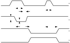
tS |
– |
Minimum Setup Time |
tH |
– |
Minimum Hold Time |
tPD |
– |
Input to Output Delay |
tPD(E) |
– |
LATCH ENABLE to Output Delay |
tPW(E) – |
Minimum LATCH ENABLE Pulsewidth |
|
VOS |
– |
Input Offset Voltage |
VOD |
– |
Overdrive Voltage |
Figure 1. System Timing Diagram
–2– |
REV. D |
AD96685/AD96687
ABSOLUTE MAXIMUM RATINGS1
Positive Supply Voltage (+VS) . . . . . . . . . . . . . . . . . . . . . 6.5 V
Negative Supply Voltage (–VS) . . . . . . . . . . . . . . . . . . . –6.5 V Input Voltage Range2 . . . . . . . . . . . . . . . . . . . . . . . . . . . . ±5 V
Differential Input Voltage . . . . . . . . . . . . . . . . . . . . . . . . 5.5 V
Latch Enable Voltage . . . . . . . . . . . . . . . . . . . . . . . . –VS to 0 V Output Current . . . . . . . . . . . . . . . . . . . . . . . . . . . . . . . 30 mA
Operating Temperature Range3 AD96685BR/AD96687BQ/BR/BP . . . . . . . –25°C to +85°C
Storage Temperature Range . . . . . . . . . . . . –55°C to +150°C Junction Temperature . . . . . . . . . . . . . . . . . . . . . . . . . . 175°C Lead Soldering Temperature (10 sec) . . . . . . . . . . . . . . 300°C
NOTES
1Absolute maximum ratings are limiting values, may be applied individually, and beyond which serviceability of the circuit may be impaired. Functional operation under any of these conditions is not necessarily implied. Exposure to absolute maximum rating conditions for extended periods may affect device reliability.
2Under no circumstances should the input voltages exceed the supply voltages.
3Typical thermal impedances . . .
AD96685 SOIC |
qJA = 170°C/W; qJC = 60°C/W |
AD96687 Ceramic |
qJA = 115°C/W; qJC = 57°C/W |
AD96687 SOIC |
qJA = 92°C/W; qJC = 47°C/W |
AD96687 PLCC |
qJA = 81°C/W; qJC = 45°C/W |
EXPLANATION OF TEST LEVELS
Test Level
I – 100% production tested.
II– 100% production tested at 25°C, and sample tested at specified temperatures.
III – Sample tested only.
IV – Parameter is guaranteed by design and characterization testing.
V – Parameter is a typical value only.
VI – All devices are 100% production tested at 25°C; 100% production tested at temperature extremes for extended temperature devices; sample tested at temperature extremes for commercial/industrial devices.
|
FUNCTIONAL DESCRIPTION |
|
|
Pin Name |
Description |
|
|
+VS |
Positive supply terminal, nominally 5.0 V. |
NONINVERTING INPUT |
Noninverting analog input of the differential input stage. The NONINVERTING INPUT must be |
|
driven in conjunction with the INVERTING INPUT. |
INVERTING INPUT |
Inverting analog input of the differential input stage. The INVERTING INPUT must be driven in |
|
conjunction with the NONINVERTING INPUT. |
LATCH ENABLE |
In the “compare” mode (logic HIGH), the output will track changes at the input of the compara- |
|
tor. In the “latch” mode (logic LOW), the output will reflect the input state just prior to the |
|
comparator being placed in the “latch” mode. LATCH ENABLE must be driven in conjunction |
|
with LATCH ENABLE for the AD96687. |
LATCH ENABLE |
In the “compare” mode (logic LOW), the output will track changes at the input of the comparator. |
|
In the “latch” mode (logic HIGH), the output will reflect the input state just prior to the comparator |
|
being placed in the “latch” mode. LATCH ENABLE must be driven in conjunction with |
|
LATCH ENABLE for the AD96687. |
–VS |
Negative supply terminal, nominally –5.2 V. |
Q |
One of two complementary outputs. Q will be at logic HIGH if the analog voltage at the |
|
NONINVERTING INPUT is greater than the analog voltage at the INVERTING INPUT (pro- |
|
vided the comparator is in the “compare” mode). See LATCH ENABLE and LATCH ENABLE |
|
(AD96687 only) for additional information. |
Q |
One of two complementary outputs. Q will be at logic LOW if the analog voltage at the |
|
NONINVERTING INPUT is greater than the analog voltage at the INVERTING INPUT |
|
(provided the comparator is in the “compare” mode). See LATCH ENABLE and LATCH ENABLE |
|
(AD96687 only) for additional information. |
GROUND 1 |
One of two grounds, but primarily associated with the digital ground. Both grounds should be |
|
connected together near the comparator. |
GROUND 2 |
One of two grounds, but primarily associated with the analog ground. Both grounds should be |
|
connected together near the comparator. |
|
|
REV. D |
–3– |
 Loading...