


AD9020TZ-883
Table of contents
 Loading...
Analog Devices AD9020TZ-883, AD9020TE-883, AD9020SZ-883, AD9020SE-883, AD9020KZ Datasheet
...
10-Bit 60 MSPS
a
FEATURES
Monolithic 10-Bit/60 MSPS Converter
TTL Outputs
Bipolar (ⴞ1.75 V) Analog Input
56 dB SNR @ 2.3 MHz Input
Low (45 pF) Input Capacitance
MIL-STD-883-Compliant Versions Available
APPLICATIONS
Digital Oscilloscopes
Medical Imaging
Professional Video
Radar Warning/Guidance Systems
Infrared Systems
GENERAL DESCRIPTION
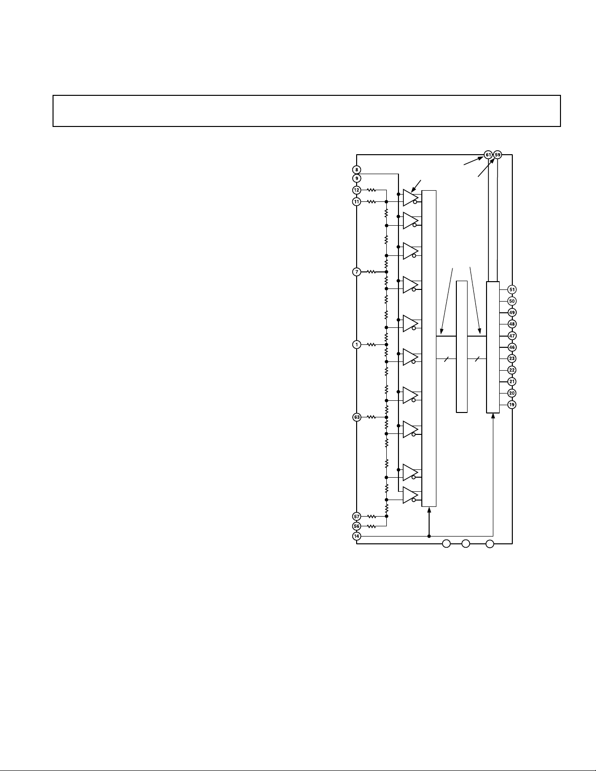
The AD9020 A/D converter is a 10-bit monolithic converter
capable of word rates of 60 MSPS and above. Innovative architecture using 512 input comparators instead of the traditional
1024 required by other flash converters reduces input capacitance and improves linearity.
Encode and outputs are TTL-compatible, making the AD9020
an ideal candidate for use in low power systems. An overflow bit is provided to indicate analog input signals greater
than +V
Voltage sense lines are provided to insure accurate driving of the
± V
REF
resistor ladder help optimize the integral linearity of the unit.
Either 68-pin ceramic leaded (gull wing) packages or ceramic
LCCs are available and are specifically designed for low thermal
impedances. Two performance grades for temperatures of both
0°C to 70°C and –55°C to +125°C ranges are offered to allow
the user to select the linearity best suited for each application.
Dynamic performance is fully characterized and production
tested at 25°C. MIL-STD-883 units are available.
The AD9020 A/D Converter is available in versions compliant
with MIL-STD-883. Refer to the Analog Devices Military Products Databook or current AD9020/883B data sheet for detailed
specifications.
.
SENSE
voltages applied to the units. Quarter-point taps on the
ANALOG IN
+V
REF
+V
SENSE
3/4
REF
1/2
REF
1/4
REF
–V
SENSE
–V
REF
ENCODE
A/D Converter
AD9020
FUNCTIONAL BLOCK DIAGRAM
MSB
C
O
M
P
A
R
A
T
O
R
L
A
T
C
H
E
S
INVERT
AD9020
OVERFLOW
1024
–V
S
LSBS
INVERT
D
E
C
O
D
E
L
O
G
I
C
+V
S
10
GROUND
L
A
T
C
H
R/2
R/2
R/2
R/2
R/2
R/2
R/2
OVERFLOW
512
R
385
384
R
R
257
256
R
R
129
128
R
R
2
R
1
R/2
OVERFLOW
D
(MSB)
9
D
8
D
7
D
6
D
5
D
4
D
3
D
2
D
1
D0 (LSB)
REV. C
Information furnished by Analog Devices is believed to be accurate and
reliable. However, no responsibility is assumed by Analog Devices for its
use, nor for any infringements of patents or other rights of third parties that
may result from its use. No license is granted by implication or otherwise
under any patent or patent rights of Analog Devices.
One Technology Way, P.O. Box 9106, Norwood, MA 02062-9106, U.S.A.
Tel: 781/329-4700 www.analog.com
Fax: 781/326-8703 © Analog Devices, Inc., 2001

AD9020–SPECIFICATIONS
ABSOLUTE MAXIMUM RATINGS
+VS . . . . . . . . . . . . . . . . . . . . . . . . . . . . . . . . . . . . . . . . . +6 V
. . . . . . . . . . . . . . . . . . . . . . . . . . . . . . . . . . . . . . . . . . –6 V
–V
S
ANALOG IN . . . . . . . . . . . . . . . . . . . . . . . . . . . –2 V to +2 V
+V
, –V
, 3/4
+V
REF
REF
REF
to –V
, 1/2
REF
. . . . . . . . . . . . . . . . . . . . . . . . . . . . . . . . 4.0 V
REF
REF
, 1/4
DIGITAL INPUTS . . . . . . . . . . . . . . . . . . . . . . .–0.5 V to +V
ELECTRICAL CHARACTERISTICS
1
. . . . . . . . . . –2 V to +2 V
REF
(ⴞVS = ⴞ5 V; ⴞV
3/4
, 1/2
, 1/4
REF
REF
Current . . . . . . . . . . . . . . . . . . . ± 10 mA
REF
Digital Output Current . . . . . . . . . . . . . . . . . . . . . . . . . 20 mA
Operating Temperature
AD9020JE/KE/JZ/KZ . . . . . . . . . . . . . . . . . . . . 0°C to 70°C
Storage Temperature . . . . . . . . . . . . . . . . . . . –65°C to +150°C
Maximum Junction Temperature
Lead Soldering Temp (10 sec) . . . . . . . . . . . . . . . . . . . . 300°C
S
= ⴞ1.75 V; ENCODE = 40 MSPS unless otherwise noted)
SENSE
2
. . . . . . . . . . . . . . . . . 150°C
Test AD9020JE/JZ AD9020KE/KZ
Parameter (Conditions) Temp Level Min Typ Max Min Typ Max Unit
RESOLUTION 10 10 Bits
DC ACCURACY
3
Differential Nonlinearity 25°C I 1.0 1.25 0.75 1.0 LSB
Full VI 1.5 1.25 LSB
Integral Nonlinearity 25°C I 1.25 2.75 1.0 2.25 LSB
Full VI 3.0 2.50 LSB
No Missing Codes Full VI Guaranteed
ANALOG INPUT
Input Bias Current
4
25°C I 0.4 1.0 0.4 1.0 mA
Full VI 2.0 2.0 mA
Input Resistance 25°C I 2.0 7.0 2.0 7.0 kΩ
Input Capacitance
4
25°C V 45 45 pF
Analog Bandwidth 25°C V 175 175 MHz
REFERENCE INPUT
Reference Ladder Resistance 25°C I 22 37 56 22 37 56 Ω
Full VI 14 66 14 66 Ω
Ladder Tempco Full V 0.1 0.1 Ω/°C
Reference Ladder Offset
Top of Ladder 25°C I 45 90 45 90 mV
Full VI 90 90 mV
Bottom of Ladder 25°C I 45 90 45 90 mV
Full VI 90 90 mV
Offset Drift Coefficient Full V 50 50 µV/°C
SWITCHING PERFORMANCE
Conversion Rate 25°C I 60 60 MSPS
Aperture Delay (t
Aperture Uncertainty (Jitter) 25° C V 5 5 ps, rms
Output Delay (t
Output Time Skew
)25°CV 1 1 ns
A
5
OD
)
5
25°C I 6 10 13 6 10 13 ns
25°CI 35 35 ns
DYNAMIC PERFORMANCE
Transient Response 25°C V 10 10 ns
Overvoltage Recovery Time 25°C V 10 10 ns
Effective Number of Bits (ENOB)
= 2.3 MHz 25°C I 7.9 9.0 7.9 9.0 Bits
f
IN
= 10.3 MHz 25°C IV 7.6 8.4 7.6 8.4 Bits
f
IN
f
= 15.3 MHz 25°C IV 7.2 8.0 7.2 8.0 Bits
IN
Signal-to-Noise Ratio
6
fIN = 2.3 MHz 25°C I 49.5 56 49.5 56 dB
f
= 10.3 MHz 25°C I 47.5 53 47.5 53 dB
IN
f
= 15.3 MHz 25°C I 45.5 50 45.5 50 dB
IN
Signal-to-Noise Ratio
6
(Without Harmonics)
f
= 2.3 MHz 25°C I 49.5 56 49.5 56 dB
IN
= 10.3 MHz 25°C I 49.5 54 49.5 54 dB
f
IN
fIN = 15.3 MHz 25°C I 48 52 48 52 dB
–2–
REV. C

AD9020
Test AD9020JE/JZ AD9020KE/KZ
Parameter (Conditions) Temp Level Min Typ Max Min Typ Max Unit
DYNAMIC PERFORMANCE (continued)
Harmonic Distortion
f
= 2.3 MHz 25°C I 54.5 67 54.5 67 dBc
IN
f
= 10.3 MHz 25°C I 48.5 59 48.5 59 dBc
IN
= 15.3 MHz 25°C I 46.5 53 46.5 53 dBc
f
IN
Two-Tone Intermodulation
Distortion Rejection
Differential Phase 25°C V 0.5 0.5 Degree
Differential Gain 25°CV 1 1 %
ENCODE INPUT
Logic “1” Voltage Full VI 2.0 2.0 V
Logic “0” Voltage Full VI 0.8 0.8 V
Logic “1” Current Full VI 500 500 µA
Logic “0” Current Full VI 800 800 µA
Input Capacitance 25°CV 5 5 pF
Pulsewidth (High) 25°CI66ns
Pulsewidth (Low) 25°CI66ns
DIGITAL OUTPUTS
Logic “1” Voltage (I
Logic “0” Voltage (IOL = 6 mA) Full VI 0.4 V
POWER SUPPLY
Supply Current 25°C I 440 530 440 530 mA
+V
S
Supply Current 25°C I 140 170 140 170 mA
–V
S
Power Dissipation 25°C I 2.8 3.3 2.8 3.3 W
Power Supply Rejection
Ratio (PSRR)
NOTES
1
Absolute maximum ratings are limiting values to be applied individually, and beyond which the service ability of the circuit may be impaired. Functional operability is
not necessarily implied. Exposure to absolute maximum rating conditions for an extended period of time may affect device reliability.
2
Typical thermal impedances (part soldered onto board): 68-pin leaded ceramic chip carrier: θJC = 1°C/W; θJA = 17°C/W (no air flow); θJA = 15°C/W
(air flow = 500 LFM). 68-pin ceramic LCC: θJC = 2.6°C/W; θJA = 15°C/W (no air flow); θJA = 13°C/W (air flow = 500 LFM).
3
3/4
, 1/2
REF
tested and not included in linearity specifications.
4
Measured with ANALOG IN = +V
5
Output delay measured as worst-case time from 50% point of the rising edge of ENCODE to 50% point of the slowest rising or falling edge of D0–D9. Output skew
measured as worst-case difference in output delay among D0–D9.
6
RMS signal to rms noise with analog input signal 1 dB below full scale at specified frequency.
7
Intermodulation measured with analog input frequencies of 2.3 MHz and 3.0 MHz at 7 dB below full scale.
8
Measured as the ratio of the worst-case change in transition voltage of a single comparator for a 5% change in +V
Specifications subject to change without notice.
, and 1/4
REF
7
= 2 mA) Full VI 2.4 2.4 V
OH
25°C V 70 70 dBc
Full VI 542 542 mA
Full VI 177 177 mA
Full VI 3.4 3.4 W
8
reference ladder taps are driven from dc sources at +0.875 V, 0 V, and –0.875 V, respectively. Accuracy of the overflow comparator is not
REF
SENSE
Full VI 6 10 6 10 mV/V
.
or –VS.
S
REV. C
–3–
AD9020
EXPLANATION OF TEST LEVELS
Test Level
I – 100% production tested.
II – 100% production tested at 25°C, and sample tested at
specified temperatures.
III – Sample tested only.
IV – Parameter is guaranteed by design and characterization
testing.
V – Parameter is a typical value only.
VI – All devices are 100% production tested at 25°C. 100%
production tested at temperature extremes for extended
temperature devices; sample tested at temperature extremes
for commercial/industrial devices.
DIE LAYOUT AND MECHANICAL INFORMATION
Die Dimensions . . . . . . . . . . . . . . . 206 ⫻ 140 ⫻ 15 (±2) mils
Pad Dimensions . . . . . . . . . . . . . . . . . . . . . . . . . . . .4 ⫻ 4 mils
Metalization . . . . . . . . . . . . . . . . . . . . . . . . . . . . . . . . . . . Gold
Backing . . . . . . . . . . . . . . . . . . . . . . . . . . . . . . . . . . . . . None
Substrate Potential . . . . . . . . . . . . . . . . . . . . . . . . . . . . . . –V
S
Passivation . . . . . . . . . . . . . . . . . . . . . . . . . . . . . . . . . . Nitride
S
GROUND
–V
REF
1/2
S
+V
S
+V
GROUND
GROUND
+V
S
+V
GROUND
GROUND
S
S
–VS–V
GROUND
+V
S
D
5
D
6
D
7
D
8
D
(MSB)
9
OVERFLOW
+V
S
GROUND
–V
S
+V
S
–V
REF
–V
SENSE
1/4
REF
NC
LSBs INVERT
MSB INVERT
S
–V
+V
D0 (LSB)
+V
GROUND
–V
+V
ENCODE
GROUND
+V
REF
+V
SENSE
D
D
D
D
S
4
3
2
1
S
S
S
S
S
–V
GROUND
–V
REF
+V
3/4
ANALOG IN
ANALOG IN
S
GROUND
+V
S
GROUND
S+VS
GROUND
+V
S
S
–V
+V
GROUND
ORDERING GUIDE
Device Range Description Option*
AD9020JZ 0°C to 70°C 68-Lead Leaded Ceramic Z-68
AD9020JE 0°C to 70°C 68-Terminal Ceramic LCC E-68A
AD9020KZ 0°C to 70°C 68-Lead Leaded Ceramic Z-68
AD9020KE 0°C to 70°C 68-Terminal Ceramic LCC E-68A
AD9020SZ/883 –55°C to +125°C 68-Lead Leaded Ceramic Z-68
AD9020SE/883 –55°C to +125°C 68-Terminal Ceramic LCC E-68A
AD9020TZ/883 –55°C to +125°C 68-Lead Leaded Ceramic Z-68
AD9020TE/883 –55°C to +125°C 68-Terminal Ceramic LCC E-68A
AD9020/PCB 0°C to 70°C Evaluation Board
*E = Ceramic Leadless Chip Carrier; Z = Ceramic Leaded Chip Carrier.
AD1
AD2
+2V
–2V
Temperature Package
5.0V
0.1F
3,6,15,18,25,30,33,34,
REF
REF
37,40,45,52,55,65,68
+V
S
AD9020
–V
S
2,16,28,29,35,
41,42,54,64
–5.2V
GROUND
0.1F
– D
D
0
D
– D
5
19
4
23
46
9
51
4,5,13,17,
27,31,32,
36,38,39,
43,53,66,67
100⍀
8
ANALOG IN
9
510⍀
14
ENCODE
+V
12
56
–V
59
LSBs INVERT
MSB INVERT
61
STATIC: AD1 = –2V; AD2 = +2.4V
DYNAMIC: AD1 = ⴞ2V TRIANGLE WAVE
AD2 = TTL PULSE TRAIN
510⍀
510⍀
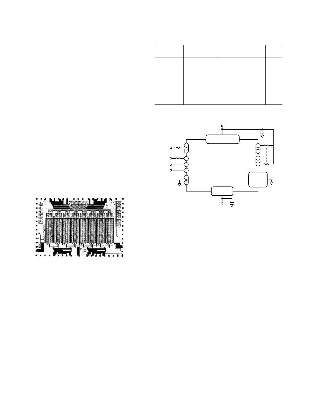
Figure 1. Burn-In Circuit
–4–
REV. C
Loading...