


Analog Devices AD7828UQ, AD7828UE, AD7824LN, AD7824KR, AD7824KN Datasheet
...a |
LC2MOS High Speed |
|
4- & 8-Channel 8-Bit ADCs |
||
|
|
AD7824/AD7828 |
FEATURES
4- or 8-Analog Input Channels Built-In Track/Hold Function
10 kHz Signal Handling on Each Channel Fast Microprocessor Interface
Single 5 V Supply
Low Power: 50 mW
Fast Conversion Rate, 2.5 s/Channel
Tight Error Specification: 1/2 LSB
|
FUNCTIONAL BLOCK DIAGRAM |
|
|||
VREF (+) |
|
4-BIT |
|
|
DB7 |
VREF (–) |
|
FLASH |
|
|
DB6 |
|
ADC |
|
|
DB5 |
|
AIN 1 |
|
(4MSB) |
|
|
DB4 |
|
|
|
|
||
AIN 4 |
MUX* |
4-BIT |
|
THREE |
|
DAC |
|
STATE |
|
||
|
VREF |
(+) |
|
DRIVERS |
|
|
|
|
DB3 |
||
|
16 |
4-BIT |
|
|
|
AIN 8 |
FLASH |
|
|
DB2 |
|
|
|
|
|||
|
|
ADC |
|
|
DB1 |
|
|
(4LSB) |
|
|
DB0 |
|
|
|
|
|
|
|
ADDRESS |
TIMING AND CONTROL |
INT |
||
|
LATCH |
||||
|
|
CIRCUITRY |
|||
|
DECODE |
|
|
||
|
|
|
|
|
|
|
A0 A1 A2** |
RDY |
CS |
RD |
|
|
|
|
|
|
|
|
*AD7824 – 4-CHANNEL MUX |
|
|
|
|
|
**AD7828 – 8-CHANNEL MUX |
|
|
|
|
|
A2 – AD7828 ONLY |
|
|
|
|
GENERAL DESCRIPTION
The AD7824 and AD7828 are high-speed, multichannel, 8-bit ADCs with a choice of 4 (AD7824) or 8 (AD7828) multiplexed analog inputs. A half-flash conversion technique gives a fast conversion rate of 2.5 s per channel and the parts have a builtin track/hold function capable of digitizing full-scale signals of 10 kHz (157 mV/ s slew rate) on all channels. The AD7824 and AD7828 operate from a single 5 V supply and have an analog input range of 0 V to 5 V, using an external 5 V reference.
Microprocessor interfacing of the parts is simple, using standard Chip Select (CS) and Read (RD) signals to initiate the conversion and read the data from the three-state data outputs. The half-flash conversion technique means that there is no need to generate a clock signal for the ADC. The AD7824 and AD7828 can be interfaced easily to most popular microprocessors.
The AD7824 and AD7828 are fabricated in an advanced, all ion-implanted, linear-compatible CMOS process (LC2MOS) and have low power dissipation of 40 mW (typ). The AD7824 is available in a 0.3" wide, 24-lead “skinny” DIP, while the AD7828 is available in a 0.6" wide, 28-lead DIP and in 28terminal surface mount packages.
PRODUCT HIGHLIGHTS
1.4- or 8-channel input multiplexer gives cost-effective spacesaving multichannel ADC system.
2.Fast conversion rate of 2.5 s/channel features a per channel sampling frequency of 100 kHz for the AD7824 or 50 kHz for the AD7828.
3.Built-in track-hold function allows handling of 4- or 8- channels up to 10 kHz bandwidth (157 mV/ s slew rate).
4.Tight total unadjusted error spec and channel-to-channel matching eliminate the need for user trims.
5.Single 5 V supply simplifies system power requirements.
6.Fast, easy-to-use digital interface allows connection to most popular microprocessors with minimal external components. No clock signal is required for the ADC.
REV. D
Information furnished by Analog Devices is believed to be accurate and reliable. However, no responsibility is assumed by Analog Devices for its use, nor for any infringements of patents or other rights of third parties which may result from its use. No license is granted by implication or otherwise under any patent or patent rights of Analog Devices.
One Technology Way, P.O. Box 9106, Norwood, MA 02062-9106, U.S.A.
Tel: 781/329-4700 |
World Wide Web Site: http://www.analog.com |
Fax: 781/326-8703 |
© Analog Devices, Inc., 2000 |
AD7824/AD7828–SPECIFICATIONS (VDD = 5 V, VREF(+) = 5 V, VREF(–) = GND = O V unless otherwise noted. All specifications TMIN to TMAX unless otherwise noted. Specifications apply for Mode 0.)
Parameter |
K Version1 |
L Version |
B, T Versions |
C, U Versions |
Unit |
Conditions/Comments |
|
|
|
|
|
|
|
|
|
ACCURACY |
|
|
|
|
|
|
|
Resolution |
8 |
8 |
8 |
8 |
Bits |
|
|
Total Unadjusted Error2 |
±1 |
±1/2 |
±1 |
±1/2 |
LSB max |
|
|
Minimum Resolution for which |
|
|
|
|
|
|
|
No Missing Codes Are Guaranteed |
8 |
8 |
8 |
8 |
Bits |
|
|
Channel-to-Channel Mismatch |
±1/4 |
±1/4 |
±1/4 |
±1/4 |
LSB max |
|
|
|
|
|
|
|
|
|
|
REFERENCE INPUT |
|
|
|
|
kΩ min/kΩ max |
|
|
Input Resistance |
1.0/4.0 |
1.0/4.0 |
1.0/4.0 |
1.0/4.0 |
|
||
VREF(+) Input Voltage Range |
VREF(–)/ |
VREF(–)/ |
VREF(–)/ |
VREF(–)/ |
V min/V max |
|
|
|
VDD |
VDD |
VDD |
VDD |
|
|
|
VREF(–) Input Voltage Range |
GND/ |
GND/ |
GND/ |
GND/ |
V min/V max |
|
|
|
VREF(+) |
VREF(+) |
VREF(+) |
VREF(+) |
|
|
|
ANALOG INPUT |
|
|
|
|
|
|
|
Input Voltage Range |
VREF(–)/ |
VREF(–)/ |
VREF(–)/ |
VREF(– )/ |
V min/V max |
|
|
|
VREF(+) |
VREF(+) |
VREF(+) |
VREF(+) |
µA max |
|
|
Input Leakage Current |
±3 |
±3 |
±3 |
±3 |
Analog Input Any Channel |
||
Input Capacitance3 |
45 |
45 |
45 |
45 |
pF typ |
0 V to 5 V |
|
LOGIC INPUTS |
|
|
|
|
|
|
|
RD, CS, A0, A1 & A2 |
|
|
|
|
|
|
|
VINH |
2.4 |
2.4 |
2.4 |
2.4 |
V min |
|
|
VINL |
0.8 |
0.8 |
0.8 |
0.8 |
V max |
|
|
IINH |
1 |
1 |
1 |
1 |
µA max |
|
|
IINL |
–1 |
–1 |
–1 |
–1 |
µA max |
|
|
Input Capacitance3 |
8 |
8 |
8 |
8 |
pF max |
Typically 5 pF |
|
LOGIC OUTPUTS |
|
|
|
|
|
|
|
DB0–DB7 & INT |
|
|
|
|
|
ISOURCE = 360 µA |
|
VOH |
4.0 |
4.0 |
4.0 |
4.0 |
V min |
||
VOL |
0.4 |
0.4 |
0.4 |
0.4 |
V max |
ISINK = 1.6 mA |
|
IOUT (DB0–DB7) |
±3 |
±3 |
±3 |
±3 |
µA max |
Floating State Leakage |
|
Output Capacitance3 |
8 |
8 |
8 |
8 |
pF max |
Typically 5 pF |
|
RDY |
|
|
|
|
|
|
|
VOL4 |
0.4 |
0.4 |
0.4 |
0.4 |
V max |
ISINK = 2.6 mA |
|
IOUT |
±3 |
±3 |
±3 |
±3 |
µA max |
Floating State Leakage |
|
Output Capacitance |
8 |
8 |
8 |
8 |
pF max |
Typically 5 pF |
|
|
|
|
|
|
|
|
|
SLEW RATE, TRACKING3 |
0.7 |
0.7 |
0.7 |
0.7 |
V/µs typ |
|
|
|
0.157 |
0.157 |
0.157 |
0.157 |
V/µs max |
|
|
|
|
|
|
|
|
|
|
POWER SUPPLY |
|
|
|
|
|
±5% for Specified |
|
VDD |
5 |
5 |
5 |
5 |
Volts |
||
5 |
|
|
|
|
|
Performance |
|
16 |
16 |
20 |
20 |
mA max |
CS = RD = 2.4 V |
||
IDD |
|||||||
Power Dissipation |
50 |
50 |
50 |
50 |
mW typ |
|
|
|
80 |
80 |
100 |
100 |
mW max |
|
|
Power Supply Sensitivity |
±1/4 |
±1/4 |
±1/4 |
±1/4 |
LSB max |
±1/16 LSB typ |
|
|
|
|
|
|
|
VDD = 5 V ± 5% |
|
NOTES |
|
|
|
|
|
|
|
1Temperature ranges are as follows: K, L Versions; 0°C to 70°C |
|
|
|
|
|||
B, C Versions; –40°C to +85°C |
|
|
|
|
|||
T, U Versions; –55°C to +125°C |
|
|
|
|
|||
2Total Unadjusted Error includes offset, full-scale and linearity errors. |
|
|
|
|
|||
3Sample tested at 25°C by Product Assurance to ensure compliance. |
|
|
|
|
|||
4RDY is an open drain output. |
|
|
|
|
|
|
|
5See Typical Performance Characteristics. |
|
|
|
|
|
|
|
Specifications subject to change without notice.
–2– |
REV. D |
|
|
|
|
|
AD7824/AD7828 |
|
|
|
|
|
|
|
|
TIMING CHARACTERISTICS1 (VDD = 5 V; VREF(+) = 5 V; VREF(–) = GND = 0 V unless otherwise noted) |
||||||
|
|
Limit at |
Limit at |
|
|
|
|
Limit at 25 C |
TMIN, TMAX |
TMIN, TMAX |
|
|
|
Parameter |
(All Grades) |
(K, L, B, C Grades) |
(T, U Grades) |
Unit |
Conditions/Comments |
|
|
|
|
|
|
|
|
tCSS |
0 |
0 |
0 |
ns min |
CS to RD Setup Time |
|
tCSH |
0 |
0 |
0 |
ns min |
CS to RD Hold Time |
|
tAS |
0 |
0 |
0 |
ns min |
Multiplexer Address Setup Time |
|
tAH |
30 |
35 |
40 |
ns min |
Multiplexer Address Hold Time |
|
2 |
40 |
60 |
60 |
ns max |
CS to RDY Delay. Pull-Up |
|
tRDY |
||||||
|
|
|
|
µs max |
Resistor 5 kΩ. |
|
tCRD |
2.0 |
2.4 |
2.8 |
Conversion Time, Mode 0 |
||
3 |
85 |
110 |
120 |
ns max |
Data Access Time after RD |
|
tACC1 |
||||||
3 |
50 |
60 |
70 |
ns max |
Data Access Time after INT, Mode 0 |
|
tACC2 |
||||||
tlNTH |
40 |
65 |
70 |
ns typ |
RD to INT Delay |
|
2 |
|
|
|
|
|
|
4 |
75 |
100 |
100 |
ns max |
|
|
60 |
70 |
70 |
ns max |
Data Hold Time |
||
tDH |
||||||
tP |
500 |
500 |
600 |
ns min |
Delay Time between Conversions |
|
tRD |
60 |
80 |
80 |
ns min |
Read Pulsewidth, Mode 1 |
|
|
600 |
500 |
400 |
ns max |
|
|
|
|
|
|
|
|
|
NOTES
1Sample tested at 25°C to ensure compliance. All input control signals are specified with tr = tf = 20 ns (10% to 90% of 5 V) and timed from a voltage level of 1.6 V. 2CL = 50 pF.
3Measured with load circuits of Figure 1 and defined as the time required for an output to cross 0.8 V or 2.4 V. 4Defined as the time required for the data lines to change 0.5 V when loaded with the circuits of Figure 2.
Specifications subject to change without notice.
Test Circuits
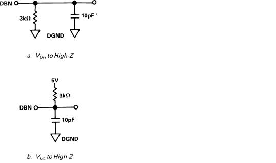
Figure 1. Load Circuits for Data Access Time Test |
Figure 2. Load Circuits for Data Hold Time Test |
|
REV. D |
–3– |

AD7824/AD7828
ABSOLUTE MAXIMUM RATINGS*
(TA = 25°C unless otherwise noted)
VDD . . . . . . . . . . . . . . . . . . . . . . . . . . . . . . . . . . . . . . 0 V, 7 V Digital Input Voltage to GND
(RD, CS, A0, A1 & A2) . . . . . . . . . . . . –0.3 V, VDD + 0.3 V Digital Output Voltage to GND
(DB0, DB7, RDY & INT) . . . . . . . . . . –0.3 V, VDD + 0.3 V VREF (+) to GND . . . . . . . . . . . . . . . . . .VREF (–), VDD + 0.3 V VREF (–) to GND . . . . . . . . . . . . . . . . . . . . . . . . 0 V, VREF (+) Analog Input (Any Channel) . . . . . . . . . . –0.3 V, VDD + 0.3 V
Operating Temperature Range |
0°C to 70°C |
Commercial (K, L Versions) . . . . . . . . . . |
|
Industrial (B, C Versions) . . . . . . . . . . . . . |
–25°C to +85°C |
Extended (T, U Versions) . . . . . . . . . . . . |
–55°C to +125°C |
Storage Temperature Range . . . . . . . . . . . . |
–65°C to +150°C |
Lead Temperature (Soldering, 10 secs) . . . . . |
. . . . . . . . 300°C |
Power Dissipation (Any Package) to 75°C . . . |
. . . . . . 450 mW |
Derates above 75°C by . . . . . . . . . . . . . . . . . |
. . . . . 6 mW/°C |
*Stresses above those listed under Absolute Maximum Ratings may cause permanent damage to the device. This is a stress rating only; functional operation of the device at these or any other conditions above those indicated in the operational sections of this specification is not implied. Exposure to absolute maximum rating conditions for extended periods may affect device reliability.
CAUTION
ESD (electrostatic discharge) sensitive device. Electrostatic charges as high as 4000 V readily accumulate on the human body and test equipment and can discharge without detection. Although these devices feature proprietary ESD protection circuitry, permanent damage may occur on devices subjected to high-energy electrostatic discharges. Therefore, proper ESD precautions are recommended to avoid performance degradation or loss of functionality.
PIN CONFIGURATIONS
DIP/SOIC/SSOP
WARNING!
ESD SENSITIVE DEVICE
LCCC
|
|
ORDERING GUIDE |
|
|
|
|
|
|
|
|
|
|
Total |
|
|
|
Temperature |
Unadjusted |
Package |
|
Model |
Range |
Error (LSBs) |
Option |
|
|
|
|
|
|
AD7824KN |
0°C to 70°C |
± 1 |
N-24 |
|
AD7824LN |
0°C to 70°C |
± 1/2 |
N-24 |
|
AD7824KR |
0°C to 70°C |
± 1 |
R-24 |
PLCC |
AD7824BQ |
–40°C to +85°C |
± 1 |
Q-24 |
AD7824CQ |
–40°C to +85°C |
± 1/2 |
Q-24 |
|
|
AD7824TQ* |
–55°C to +125°C |
± 1 |
Q-24 |
|
AD7824UQ* |
–55°C to +125°C |
± 1/2 |
Q-24 |
|
AD7828KN |
0°C to 70°C |
± 1 |
N-28 |
|
AD7828LN |
0°C to 70°C |
± 1/2 |
N-28 |
|
AD7828KP |
0°C to 70°C |
± 1 |
P-28A |
|
AD7828LP |
0°C to 70°C |
± 1/2 |
P-28A |
|
AD7828BQ |
–40°C to +85°C |
± 1 |
Q-28 |
|
AD7828CQ |
–40°C to +85°C |
± 1/2 |
Q-28 |
|
AD7828BR |
–40°C to +85°C |
+1 |
R-28 |
|
AD7828BRS |
–40°C to +85°C |
+1 |
RS-28 |
|
AD7828TQ* |
–55°C to +125°C |
± 1 |
Q-28 |
|
AD7828UQ* |
–55°C to +125°C |
± 1/2 |
Q-28 |
|
AD7828TE* |
–55°C to +125°C |
± 1 |
E-28A |
|
AD7828UE* |
–55°C to +125°C |
± 1/2 |
E-28A |
*Available to /883B processing only. Contact our local sales office for military data sheet. For U.S. Standard Military Drawing (SMD) see DESC Drawing #5692-88764.
–4– |
REV. D |
 Loading...