


 Loading...
Analog Devices AD977CRS, AD977CR, AD977CN, AD977BRS, AD977BR Datasheet
...a |
16-Bit, 100 kSPS/200 kSPS |
|
BiCMOS A/D Converter |
||
|
|
|
|
|
AD977/AD977A |
|
|
|
FEATURES Fast 16-Bit ADC
100 kSPS Throughput Rate—AD977
200 kSPS Throughput Rate—AD977A Single 5 V Supply Operation
Power Dissipation 100 mW Max Power-Down Mode 50 W
Input Ranges:
Unipolar; 0 V–10 V, 0 V–5 V and 0 V–4 V Bipolar; 10 V, 5 V and 3.3 V
Choice of External or Internal 2.5 V Reference High Speed Serial Interface
On-Chip Clock
20-Lead Skinny DIP or SOIC Package
28-Lead Skinny SSOP Package
FUNCTIONAL BLOCK DIAGRAM
|
|
REF |
|
|
VANA |
AGND1 |
|
|
|
|
|
4k |
|
2.5V |
|
AD977/ |
|
CAP |
|
|
|
|
|
|
||
|
|
|
REFERENCE |
AD977A |
|
|||
|
4R |
|
|
|
||||
R1IN |
|
|
|
|
|
|
||
|
|
|
|
|
|
|
SYNC |
|
|
2R |
|
|
|
|
|
|
|
R2IN |
|
|
|
|
|
SERIAL |
BUSY |
|
|
|
|
|
|
|
|||
R3IN |
R |
4R |
|
SWITCHED |
|
DATA |
DATACLK |
|
|
CAP ADC |
INTERFACE |
||||||
|
|
|
DATA |
|||||
|
|
|
|
|
|
|
|
|
AGND2 |
R = 5k AD977 |
|
|
|
|
|
|
|
R = 2.5k AD977A |
|
|
|
|
|
|||
|
|
|
|
|
|
|||
VDIG |
|
CONTROL LOGIC & |
|
CLOCK |
|
|||
INTERNAL CALIBRATION CIRCUITRY |
|
|||||||
|
|
|
||||||
|
DGND |
PWRD |
R/C |
CS |
TAG |
SB/BTC EXT/INT |
|
|
GENERAL DESCRIPTION
The AD977/AD977A is a high speed, low power 16-bit A/D converter that operates from a single 5 V supply. The AD977A has a throughput rate of 200 kSPS whereas the AD977 has a throughput rate of 100 kSPS. Each part contains a successive approximation, switched capacitor ADC, an internal 2.5 V reference, and a high speed serial interface. The ADC is factory calibrated to minimize all linearity errors. The AD977/AD977A is specified for full scale bipolar input ranges of ± 10 V, ±5 V and
± 3.3 V, and unipolar ranges of 0 V to 10 V, 0 V to 5 V and 0 V to 4 V.
The AD977/AD977A is comprehensively tested for ac parameters such as SNR and THD, as well as the more traditional dc parameters of offset, gain and linearity.
PRODUCT HIGHLIGHTS
1.Fast Throughput
The AD977/AD977A is a high speed, 16-bit ADC based on a factory calibrated switched capacitor architecture.
2.Single-Supply Operation
The AD977/AD977A operates from a single 5 V supply and dissipates only 100 mW max.
3.Comprehensive DC and AC Specifications
In addition to the traditional specifications of offset, gain and linearity, the AD977/AD977A is fully tested for SNR and THD.
REV. D
Information furnished by Analog Devices is believed to be accurate and reliable. However, no responsibility is assumed by Analog Devices for its use, nor for any infringements of patents or other rights of third parties which may result from its use. No license is granted by implication or otherwise under any patent or patent rights of Analog Devices.
One Technology Way, P.O. Box 9106, Norwood, MA 02062-9106, U.S.A.
Tel: 781/329-4700 |
World Wide Web Site: http://www.analog.com |
Fax: 781/326-8703 |
© Analog Devices, Inc., 2000 |
AD977/AD977A
AD977–SPECIFICATIONS (–40 C to +85 C, FS = 100 kHz, VDIG = VANA = 5 V, unless otherwise noted)
|
|
A Grade |
|
|
|
|
B Grade |
|
|
C Grade |
|
|
Parameter |
Min |
Typ |
Max |
|
|
Min |
Typ |
Max |
Min |
Typ |
Max |
Unit |
|
|
|
|
|
|
|
|
|
|
|
|
|
RESOLUTION |
16 |
|
|
|
16 |
|
|
16 |
|
|
Bits |
|
ANALOG INPUT |
|
|
|
|
|
|
|
|
|
|
|
|
|
|
|
±10 V, 0 V to 5 V, . . . (See Table II) |
|
|
|
|
|||||
Voltage Range |
|
|
|
|
|
|
|
|||||
Impedance |
|
|
|
|
|
See Table II |
|
|
|
|
|
|
|
|
|
|
|
|
|
|
|
|
|||
Sampling Capacitance |
|
40 |
|
|
|
|
40 |
|
|
40 |
|
pF |
THROUGHPUT SPEED |
|
|
|
|
|
|
|
|
|
|
|
s |
Complete Cycle |
|
|
10 |
|
|
|
|
10 |
|
|
10 |
|
Throughput Rate |
100 |
|
|
|
100 |
|
|
100 |
|
|
kHz |
|
DC ACCURACY |
|
|
±3 |
|
|
|
|
±2.0 |
|
±3 |
|
LSB1 |
Integral Linearity Error |
|
|
|
|
|
|
|
|
||||
Differential Linearity Error |
–2 |
|
+3 |
|
|
–1 |
|
+1.75 |
|
±2 |
|
LSB |
No Missing Codes |
15 |
|
|
|
16 |
|
|
|
15 |
|
Bits |
|
Transition Noise2 |
|
1.0 |
±0.5 |
|
|
|
1.0 |
±0.25 |
|
1.0 |
±0.5 |
LSB |
Full-Scale Error3, 4 |
|
±7 |
|
|
|
±7 |
|
±7 |
% |
|||
Full-Scale Error Drift |
|
|
|
|
|
|
|
|
ppm/°C |
|||
Full-Scale Error |
|
|
±0.5 |
|
|
|
|
±0.25 |
|
|
±0.5 |
|
Ext. REF = 2.5 V |
|
|
|
|
|
|
|
|
% |
|||
Full-Scale Error Drift |
|
±2 |
|
|
|
|
±2 |
|
|
±2 |
|
ppm/°C |
Ext. REF = 2.5 V |
|
|
|
|
|
|
|
|
||||
Bipolar Zero Error3 |
|
|
±10 |
|
|
|
|
±10 |
|
|
±15 |
|
Bipolar Ranges |
|
|
|
|
|
|
|
|
mV |
|||
Bipolar Zero Error Drift |
|
±2 |
|
|
|
|
±2 |
|
|
±2 |
|
ppm/°C |
Bipolar Ranges |
|
|
|
|
|
|
|
|
||||
Unipolar Zero Error3 |
|
|
±10 |
|
|
|
|
±10 |
|
|
±10 |
|
Unipolar Ranges |
|
|
|
|
|
|
|
|
mV |
|||
Unipolar Zero Error Drift |
|
±2 |
|
|
|
|
±2 |
|
|
±2 |
|
ppm/°C |
Unipolar Ranges |
|
|
|
|
|
|
|
|
||||
Recovery to Rated Accuracy |
|
|
|
|
|
|
|
|
|
|
|
|
After Power-Down5 |
|
|
|
|
|
|
|
|
|
|
|
|
2.2 F to CAP |
|
1 |
|
|
|
|
1 |
|
|
1 |
|
ms |
Power Supply Sensitivity |
|
|
|
|
|
|
|
|
|
|
|
|
VANA = VDIG = VD = 5 V ± 5% |
|
|
±8 |
|
|
|
|
±8 |
|
|
±8 |
LSB |
AC ACCURACY |
|
|
|
|
|
|
|
|
|
|
|
|
Spurious Free Dynamic Range6 |
90 |
|
|
|
96 |
|
|
90 |
|
|
dB7 |
|
Total Harmonic Distortion6 |
|
|
–90 |
|
|
|
|
–96 |
|
|
–90 |
dB |
Signal-to-(Noise+Distortion)6 |
83 |
|
|
|
85 |
|
|
83 |
|
|
dB |
|
–60 dB Input |
|
27 |
|
|
|
|
28 |
|
|
27 |
|
dB |
Signal-to-Noise6 |
83 |
|
|
|
85 |
|
|
83 |
|
|
dB |
|
Full Power Bandwidth8 |
|
700 |
|
|
|
|
700 |
|
|
700 |
|
kHz |
–3 dB Input Bandwidth |
|
1.5 |
|
|
|
|
1.5 |
|
|
1.5 |
|
MHz |
SAMPLING DYNAMICS |
|
|
|
|
|
|
|
|
|
|
|
|
Aperture Delay |
|
40 |
|
|
|
|
40 |
|
|
40 |
|
ns |
Transient Response, Full-Scale Step |
|
|
2 |
|
|
|
|
2 |
|
|
2 |
s |
Overvoltage Recovery9 |
|
150 |
|
|
|
|
150 |
|
|
150 |
|
ns |
REFERENCE |
|
|
|
|
|
|
|
|
|
|
|
|
Internal Reference Voltage |
2.48 |
2.5 |
2.52 |
|
2.48 |
2.5 |
2.52 |
2.48 |
2.5 |
2.52 |
V |
|
Internal Reference Source Current |
|
1 |
|
|
|
|
1 |
|
|
1 |
|
A |
External Reference Voltage Range |
|
|
|
|
|
|
|
|
|
|
|
|
for Specified Linearity |
2.3 |
2.5 |
2.7 |
|
2.3 |
2.5 |
2.7 |
2.3 |
2.5 |
2.7 |
V |
|
External Reference Current Drain |
|
|
|
|
|
|
|
|
|
|
|
A |
Ext. REF = 2.5 V |
|
|
100 |
|
|
|
|
100 |
|
|
100 |
|
NOTES
1LSB means Least Significant Bit. With a ±10 V input, one LSB is 305 µV. 2Typical rms noise at worst case transitions and temperatures.
3Measured with fixed resistors as shown in Figures 11, 12 and 13. Adjustable to zero. Tested at room temperature.
4Full-Scale Error is expressed as the % difference between the actual full-scale code transition voltage and the ideal full scale transition voltage, and includes the effect of offset error. For bipolar input ranges, the Full-Scale Error is the worst case of either the –Full Scale or +Full Scale code transition voltage errors. For unipolar input ranges, Full-Scale Error is with respect to the +Full-Scale code transition voltage.
5External 2.5 V reference connected to REF.
6fIN = 20 kHz, 0.5 dB down unless otherwise noted.
7All specifications in dB are referred to a full scale ±10 V input.
8Full-Power Bandwidth is defined as full-scale input frequency at which Signal-to-(Noise+Distortion) degrades to 60 dB, or 10 bits of accuracy. 9Recovers to specified performance after a 2 × FS input overvoltage.
Specifications subject to change without notice.
–2– |
REV. D |
AD977/AD977A
AD977A–SPECIFICATIONS(–40 C to +85 C, FS = 200 kHz, VDIG = VANA = 5 V, unless otherwise noted)
|
|
A Grade |
|
|
|
|
B Grade |
|
|
C Grade |
|
|
Parameter |
Min |
Typ |
Max |
|
|
Min |
Typ |
Max |
Min |
Typ |
Max |
Unit |
|
|
|
|
|
|
|
|
|
|
|
|
|
RESOLUTION |
16 |
|
|
|
16 |
|
|
16 |
|
|
Bits |
|
ANALOG INPUT |
|
|
|
|
|
|
|
|
|
|
|
|
|
|
|
±10 V, 0 V to 5 V, . . . (See Table II) |
|
|
|
|
|||||
Voltage Range |
|
|
|
|
|
|
|
|||||
Impedance |
|
|
|
|
|
See Table II |
|
|
|
|
|
|
|
|
|
|
|
|
|
|
|
|
|||
Sampling Capacitance |
|
40 |
|
|
|
|
40 |
|
|
40 |
|
pF |
THROUGHPUT SPEED |
|
|
|
|
|
|
|
|
|
|
|
s |
Complete Cycle |
|
|
5 |
|
|
|
|
5 |
|
|
5 |
|
Throughput Rate |
200 |
|
|
|
200 |
|
|
200 |
|
|
kHz |
|
DC ACCURACY |
|
|
±3 |
|
|
|
|
±2.0 |
|
±3 |
|
LSB1 |
Integral Linearity Error |
|
|
|
|
|
|
|
|
||||
Differential Linearity Error |
–2 |
|
+3 |
|
|
–1 |
|
+1.75 |
|
±2 |
|
LSB |
No Missing Codes |
15 |
|
|
|
16 |
|
|
|
15 |
|
Bits |
|
Transition Noise2 |
|
1.0 |
±0.5 |
|
|
|
1.0 |
±0.25 |
|
1.0 |
±0.5 |
LSB |
Full-Scale Error3, 4 |
|
±7 |
|
|
|
±7 |
|
±7 |
% |
|||
Full-Scale Error Drift |
|
|
|
|
|
|
|
|
ppm/°C |
|||
Full-Scale Error |
|
|
±0.5 |
|
|
|
|
±0.25 |
|
|
±0.5 |
|
Ext. REF = 2.5 V |
|
|
|
|
|
|
|
|
% |
|||
Full-Scale Error Drift |
|
±2 |
|
|
|
|
±2 |
|
|
±2 |
|
ppm/°C |
Ext. REF = 2.5 V |
|
|
|
|
|
|
|
|
||||
Bipolar Zero Error3 |
|
|
±10 |
|
|
|
|
±10 |
|
|
±15 |
|
Bipolar Ranges |
|
|
|
|
|
|
|
|
mV |
|||
Bipolar Zero Error Drift |
|
±2 |
|
|
|
|
±2 |
|
|
±2 |
|
ppm/°C |
Bipolar Ranges |
|
|
|
|
|
|
|
|
||||
Unipolar Zero Error3 |
|
|
±10 |
|
|
|
|
±10 |
|
|
±10 |
|
Unipolar Ranges |
|
|
|
|
|
|
|
|
mV |
|||
Unipolar Zero Error Drift |
|
±2 |
|
|
|
|
±2 |
|
|
±2 |
|
ppm/°C |
Unipolar Ranges |
|
|
|
|
|
|
|
|
||||
Recovery to Rated Accuracy |
|
|
|
|
|
|
|
|
|
|
|
|
After Power-Down5 |
|
|
|
|
|
|
|
|
|
|
|
|
2.2 F to CAP |
|
1 |
|
|
|
|
1 |
|
|
1 |
|
ms |
Power Supply Sensitivity |
|
|
|
|
|
|
|
|
|
|
|
|
VANA = VDIG = VD = 5 V ± 5% |
|
|
±8 |
|
|
|
|
±8 |
|
|
±8 |
LSB |
AC ACCURACY |
|
|
|
|
|
|
|
|
|
|
|
|
Spurious Free Dynamic Range6 |
90 |
|
|
|
96 |
|
|
90 |
|
|
dB7 |
|
Total Harmonic Distortion6 |
|
|
–90 |
|
|
|
|
–96 |
|
|
–90 |
dB |
Signal-to-(Noise+Distortion)6 |
83 |
|
|
|
85 |
|
|
83 |
|
|
dB |
|
–60 dB Input |
|
27 |
|
|
|
|
28 |
|
|
27 |
|
dB |
Signal-to-Noise6 |
83 |
|
|
|
85 |
|
|
83 |
|
|
dB |
|
Full Power Bandwidth8 |
|
1 |
|
|
|
|
1 |
|
|
1 |
|
MHz |
–3 dB Input Bandwidth |
|
2.7 |
|
|
|
|
2.7 |
|
|
2.7 |
|
MHz |
SAMPLING DYNAMICS |
|
|
|
|
|
|
|
|
|
|
|
|
Aperture Delay |
|
40 |
|
|
|
|
40 |
|
|
40 |
|
ns |
Transient Response, Full-Scale Step |
|
|
1 |
|
|
|
|
1 |
|
|
1 |
s |
Overvoltage Recovery9 |
|
150 |
|
|
|
|
150 |
|
|
150 |
|
ns |
REFERENCE |
|
|
|
|
|
|
|
|
|
|
|
|
Internal Reference Voltage |
2.48 |
2.5 |
2.52 |
|
2.48 |
2.5 |
2.52 |
2.48 |
2.5 |
2.52 |
V |
|
Internal Reference Source Current |
|
1 |
|
|
|
|
1 |
|
|
1 |
|
A |
External Reference Voltage Range |
|
|
|
|
|
|
|
|
|
|
|
|
for Specified Linearity |
2.3 |
2.5 |
2.7 |
|
2.3 |
2.5 |
2.7 |
2.3 |
2.5 |
2.7 |
V |
|
External Reference Current Drain |
|
|
|
|
|
|
|
|
|
|
|
|
Ext. REF = 2.5 V |
|
|
1.2 |
|
|
|
|
1.2 |
|
|
1.2 |
mA |
NOTES
1LSB means Least Significant Bit. With a ±10 V input, one LSB is 305 µV. 2Typical rms noise at worst case transitions and temperatures.
3Measured with fixed resistors as shown in Figures 11, 12 and 13. Adjustable to zero. Tested at room temperature.
4Full-Scale Error is expressed as the % difference between the actual full-scale code transition voltage and the ideal full scale transition voltage, and includes the effect of offset error. For bipolar input ranges, the Full-Scale Error is the worst case of either the –Full Scale or +Full Scale code transition voltage errors. For unipolar input ranges, Full-Scale Error is with respect to the +Full-Scale code transition voltage.
5External 2.5 V reference connected to REF.
6fIN = 20 kHz, 0.5 dB down unless otherwise noted.
7All specifications in dB are referred to a full scale ±10 V input.
8Full-Power Bandwidth is defined as full-scale input frequency at which Signal-to-(Noise+Distortion) degrades to 60 dB, or 10 bits of accuracy. 9Recovers to specified performance after a 2 × FS input overvoltage.
Specifications subject to change without notice.
REV. D |
–3– |
AD977/AD977A–SPECIFICATIONS (Both Specs)
|
|
|
|
|
A, B, C Grades |
|
|
|
|
|
Parameter |
|
Conditions |
Min |
Typ |
|
Max |
|
|
Unit |
|
|
|
|
|
|
|
|
|
|
|
|
DIGITAL INPUTS |
|
|
|
|
|
|
|
|
|
|
Logic Levels |
|
|
|
|
|
|
|
|
|
|
VIL |
|
|
|
–0.3 |
|
|
+0.8 |
|
|
V |
VIH |
|
|
|
2.0 |
|
|
VDIG + 0.3 |
V |
||
IIL |
|
|
|
|
|
|
± 10 |
|
|
A |
IIH |
|
|
|
|
|
|
± 10 |
|
|
A |
DIGITAL OUTPUTS |
|
|
|
|
|
|
|
|
|
|
Data Format |
|
|
|
|
Serial 16-Bits |
|
|
|
|
|
Data Coding |
|
|
|
|
Binary Two’s Complement or Straight Binary |
|
||||
Pipeline Delay |
|
|
|
Conversion Results Only Available after Completed Conversion |
|
|||||
VOL |
|
ISINK = 1.6 mA |
|
|
|
0.4 |
|
|
V |
|
VOH |
|
ISOURCE = 500 A |
4 |
|
|
|
|
|
V |
|
POWER SUPPLIES |
|
|
|
|
|
|
|
|
|
|
Specified Performance |
|
|
|
|
|
|
|
|
|
|
VDIG |
|
|
|
4.75 |
5 |
|
5.25 |
|
|
V |
VANA |
|
|
|
4.75 |
5 |
|
5.25 |
|
|
V |
IDIG |
|
|
|
|
4 |
|
|
|
|
mA |
IANA |
|
|
|
|
11 |
|
|
|
|
mA |
Power Dissipation |
|
|
|
|
|
|
|
|
|
|
PWRD LOW |
|
|
|
|
|
|
100 |
|
|
mW |
PWRD HIGH |
|
|
|
|
50 |
|
|
|
|
W |
TEMPERATURE RANGE |
|
|
|
|
|
|
|
|
|
°C |
Specified Performance |
|
TMIN to TMAX |
–40 |
|
|
+85 |
|
|
||
Specifications subject to change without notice. |
|
|
|
|
|
|
|
|||
TIMING SPECIFICATIONS (AD977A: FS = 200 kHz, AD977: FS = 100 kHz, VDIG = VANA = 5 V, –40 C to +85 C) |
|
|
|
|||||||
|
|
|
|
|
|
|
|
|
|
|
|
|
|
|
|
AD977A |
|
AD977 |
|
|
|
|
|
|
|
Symbol |
Min Typ |
Max |
Min Typ |
Max |
|
Unit |
|
|
|
|
|
|
|
|
|
|
|
Convert Pulsewidth |
|
|
t1 |
50 |
|
50 |
|
|
ns |
|
R/C, CS to BUSY Delay |
|
|
t2 |
|
83 |
|
83 |
|
ns |
|
BUSY LOW Time |
|
|
t3 |
|
4.0 |
|
8.0 |
|
s |
|
BUSY Delay after End of Conversion |
|
t4 |
50 |
|
50 |
|
|
ns |
||
Aperture Delay |
|
|
t5 |
40 |
|
40 |
|
|
ns |
|
Conversion Time |
|
|
t6 |
3.8 |
4.0 |
7.6 |
8.0 |
|
s |
|
Acquisition Time |
|
|
t7 |
1.0 |
|
2.0 |
|
|
s |
|
Throughput Time |
|
|
t6 + t7 |
|
5 |
|
10 |
|
s |
|
R/C Low to DATACLK Delay |
|
|
t8 |
220 |
|
350 |
|
|
ns |
|
DATACLK Period |
|
|
t9 |
220 |
|
450 |
|
|
ns |
|
DATA Valid Setup Time |
|
|
t10 |
50 |
|
100 |
|
|
ns |
|
DATA Valid Hold Time |
|
|
t11 |
20 |
|
20 |
|
|
ns |
|
EXT. DATACLK Period |
|
|
t12 |
66 |
|
100 |
|
|
ns |
|
EXT. DATACLK HIGH |
|
|
t13 |
20 |
|
20 |
|
|
ns |
|
EXT. DATACLK LOW |
|
|
t14 |
30 |
|
30 |
|
|
ns |
|
R/C, CS to EXT. DATACLK Setup Time |
|
t15 |
20 |
t12 + 5 |
20 |
t12 + 5 |
|
ns |
||
R/C to CS Setup Time |
|
|
t16 |
10 |
|
10 |
|
|
ns |
|
EXT. DATACLK to SYNC Delay |
|
|
t17 |
15 |
66 |
15 |
66 |
|
ns |
|
EXT. DATACLK to DATA Valid Delay |
|
t18 |
25 |
66 |
25 |
66 |
|
ns |
||
CS to EXT. DATACLK Rising Edge Delay |
|
t19 |
10 |
|
10 |
|
|
ns |
||
Previous DATA Valid after CS, R/C Low |
|
t20 |
3.5 |
|
7.5 |
|
|
s |
||
BUSY to EXT. DATACLK Setup Time |
|
t21 |
5 |
|
5 |
|
|
ns |
||
Final EXT. DATACLK to BUSY Rising Edge |
|
t22 |
|
1.7 |
|
3.5 |
|
s |
||
TAG Valid Setup Time |
|
|
t23 |
0 |
|
0 |
|
|
ns |
|
TAG Valid Hold Time |
|
|
t24 |
20 |
|
20 |
|
|
ns |
|
Specifications subject to change without notice.
–4– |
REV. D |
AD977/AD977A
ABSOLUTE MAXIMUM RATINGS1
Analog Inputs
R1IN, R2IN , R3IN . . . . . . . |
. . . . . . |
. . . . . . . . . . . . . . . ±25 V |
CAP . . . . . . . . . . . . . . . . . |
+VANA + 0.3 V to AGND2 – 0.3 V |
|
REF . . . . . . . . . . . . . . . . . |
. . . . Indefinite Short to AGND2, |
|
Ground. . .Voltage. . . . . .Differences. . . . . . . . . . |
. . . . . . |
Momentary Short to VANA |
|
±0.3 V |
|
DGND, AGND1, AGND2 . . . . . . |
||
Supply Voltages |
|
|
VANA . . . . . . . . . . . . . . . . |
. . . . . . . |
. . . . . . . . . . . . . . . . 7 V |
VDIG to VANA . . . . . . . . . . |
. . . . . . . |
. . . . . . . . . . . . . . . ±7 V |
VDIG . . . . . . . . . . . . . . . . |
. . . . . . . |
. . . . . . . . . . . . . . . . 7 V |
Digital Inputs . . . . . . . . . . . |
. . . . . . . |
. –0.3 V to VDIG + 0.3 V |
Internal Power Dissipation2 |
|
|
PDIP (N), SOIC (R), SSOP (RS) . |
. . . . . . . . . . . . 700 mW |
|
Junction Temperature . . . . . |
. . . . . . . |
. . . . . . . . . . . . . . 150°C |
Storage Temperature Range N, R . . . |
. . . . . –65°C to +150°C |
|
Lead Temperature Range |
|
300°C |
(Soldering 10 sec) . . . . . . |
. . . . . . . |
|
NOTES
1Stresses above those listed under Absolute Maximum Ratings may cause permanent damage to the device. This is a stress rating only; functional operation of the device at these or any other conditions above those indicated in the operational section of this specification is not implied. Exposure to absolute maximum rating conditions for extended periods may affect device reliability.
2Specification is for device in free air:
20-Lead PDIP: θJA = 100°C/W, θJC = 31°C/W,
20-Lead SOIC: θJA = 75°C/W, θJC = 24°C/W,
28-Lead SSOP: θJA = 109°C/W, θJC = 39°C/W.
|
|
|
|
|
|
|
PIN CONFIGURATIONS |
|
|
|
|
|
|
|||||||||||||
|
|
|
SOIC and DIP |
|
|
|
|
|
|
|
|
|
|
|
SSOP |
|
|
|
|
|
|
|||||
|
|
|
|
|
|
|
|
|
|
|
|
|
|
|
|
|
|
|
|
|||||||
|
|
|
|
|
|
|
|
|
|
|
|
|
|
|
|
|
|
|
|
|
|
|
|
|
|
|
R1IN |
1 |
|
|
|
20 |
VDIG |
R1IN |
1 |
|
28 |
VDIG |
|||||||||||||||
|
|
|
|
|
|
|
|
|
|
|
|
|
|
|
|
|
|
|
|
|||||||
|
|
|
|
|
|
|
|
|
|
|
|
|
|
AGND1 |
2 |
|
27 |
VANA |
||||||||
AGND1 |
2 |
|
|
|
19 |
VANA |
|
|||||||||||||||||||
|
|
|
|
|
|
|
|
|
|
|
|
|
||||||||||||||
|
|
|
|
|
|
|
|
|
|
|
|
|
|
R2IN |
3 |
|
26 |
PWRD |
||||||||
R2IN |
3 |
|
|
|
18 |
PWRD |
|
|||||||||||||||||||
|
|
|
|
|
|
|
|
|
|
|
||||||||||||||||
|
|
|
|
|
|
|
|
|
|
|
|
|
|
R3IN |
4 |
|
25 |
BUSY |
||||||||
R3IN |
4 |
AD977 |
17 |
BUSY |
|
|
|
|
|
|
|
|
|
|
|
|
|
|||||||||
|
|
|
|
|
|
|
|
|
|
|
|
|
||||||||||||||
|
|
|
|
5 |
AD977A |
16 |
|
|
|
|
|
|
|
NC |
5 |
|
24 CS |
|||||||||
CAP |
CS |
|
||||||||||||||||||||||||
|
|
|
|
|
|
|
|
|
|
|
|
|
||||||||||||||
|
|
|
|
|
TOP VIEW |
|
|
|
|
|
|
CAP |
6 |
AD977 |
23 |
NC |
||||||||||
|
|
|
|
|
|
|
|
|
|
|
||||||||||||||||
REF |
6 |
(Not to Scale) |
15 |
R/C |
REF |
7 |
AD977A |
22 |
NC |
|||||||||||||||||
|
|
|
|
|
|
|
|
|
|
|
||||||||||||||||
AGND2 |
7 |
|
|
|
14 |
TAG |
|
|
NC |
8 |
TOP VIEW |
21 |
|
|
|
|
|
|||||||||
|
|
|
|
|
|
|
|
|
|
|
|
|
|
|
|
(Not to Scale) |
R/C |
|||||||||
SB/BTC |
8 |
|
|
|
13 |
DATA |
AGND2 |
9 |
|
20 |
NC |
|||||||||||||||
|
|
|
|
|
|
|
|
|
|
|
|
|
|
|
||||||||||||
EXT/INT |
|
9 |
|
|
|
12 |
DATACLK |
|
|
NC |
10 |
|
19 |
TAG |
||||||||||||
|
|
|
|
|
|
|
|
|
|
|
|
|
|
|
|
|
||||||||||
DGND |
10 |
|
|
|
11 |
SYNC |
|
|
NC |
11 |
|
18 |
NC |
|||||||||||||
|
|
|
|
|
|
|
|
|
|
|
|
|
|
|
|
|
|
|
|
|
|
|
|
|
|
|
|
|
|
|
|
|
|
|
|
|
|
|
|
|
|
|
|
|
|
|
|
|
|
|
|
|
|
|
|
|
|
|
|
|
|
|
|
|
|
|
|
SB/BTC |
|
12 |
|
17 |
DATA |
|||||||
|
|
|
|
|
|
|
|
|
|
|
|
|
|
|
|
|
|
|
|
|
|
|
|
|
|
|
|
|
|
|
|
|
|
|
|
|
|
|
|
|
EXT/INT |
|
13 |
|
16 |
DATACLK |
|||||||
|
|
|
|
|
|
|
|
|
|
|
|
|
|
|
|
|
|
|
|
|
SYNC |
|||||
|
|
|
|
|
|
|
|
|
|
|
|
|
|
DGND |
14 |
|
15 |
|||||||||
|
|
|
|
|
|
|
|
|
|
|
|
|
|
|
|
|
|
|
|
|
|
|
|
|
|
|
|
|
|
|
|
|
|
|
|
|
|
|
|
|
|
|
|
|
|
NC = NO CONNECT |
|
|
|
|
|
||
1.6mA  IOL
IOL
TO OUTPUT
PIN


 1.4V CL
100pF
500 A  IOH
IOH
Figure 1. Load Circuit for Digital Interface Timing
ORDERING GUIDE
|
Temperature |
Throughput |
|
|
Package |
Model |
Range |
Rate |
Max INL |
Min S/(N+D) |
Options* |
|
|
|
|
|
|
AD977AN |
–40°C to +85°C |
100 kSPS |
± 3.0 LSB |
83 dB |
N-20 |
AD977BN |
–40°C to +85°C |
100 kSPS |
± 2.0 LSB |
85 dB |
N-20 |
AD977CN |
–40°C to +85°C |
100 kSPS |
± 3.0 LSB |
83 dB |
N-20 |
AD977AAN |
–40°C to +85°C |
200 kSPS |
83 dB |
N-20 |
|
AD977ABN |
–40°C to +85°C |
200 kSPS |
± 2.0 LSB |
85 dB |
N-20 |
AD977ACN |
–40°C to +85°C |
200 kSPS |
|
83 dB |
N-20 |
AD977AR |
–40°C to +85°C |
100 kSPS |
± 3.0 LSB |
83 dB |
R-20 |
AD977BR |
–40°C to +85°C |
100 kSPS |
± 2.0 LSB |
85 dB |
R-20 |
AD977CR |
–40°C to +85°C |
100 kSPS |
± 3.0 LSB |
83 dB |
R-20 |
AD977AAR |
–40°C to +85°C |
200 kSPS |
83 dB |
R-20 |
|
AD977ABR |
–40°C to +85°C |
200 kSPS |
± 2.0 LSB |
85 dB |
R-20 |
AD977ACR |
–40°C to +85°C |
200 kSPS |
|
83 dB |
R-20 |
AD977ARS |
–40°C to +85°C |
100 kSPS |
± 3.0 LSB |
83 dB |
RS-28 |
AD977BRS |
–40°C to +85°C |
100 kSPS |
± 2.0 LSB |
85 dB |
RS-28 |
AD977CRS |
–40°C to +85°C |
100 kSPS |
± 3.0 LSB |
83 dB |
RS-28 |
AD977AARS |
–40°C to +85°C |
200 kSPS |
83 dB |
RS-28 |
|
AD977ABRS |
–40°C to +85°C |
200 kSPS |
± 2.0 LSB |
85 dB |
RS-28 |
AD977ACRS |
–40°C to +85°C |
200 kSPS |
|
83 dB |
RS-28 |
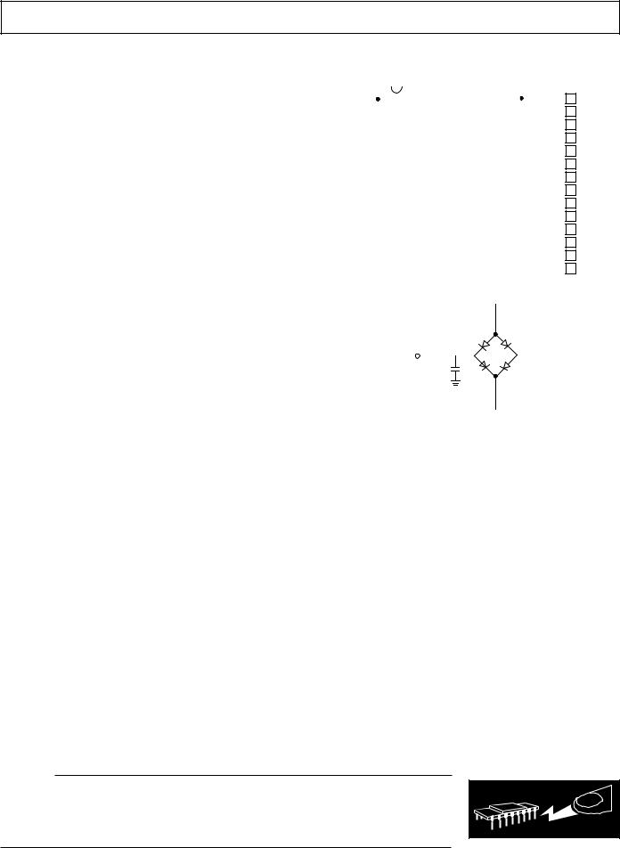
*N = 20-lead 300 mil plastic DIP; R = 20-lead SOIC; RS = 28-lead SSOP.
CAUTION
ESD (electrostatic discharge) sensitive device. Electrostatic charges as high as 4000 V readily accumulate on the human body and test equipment and can discharge without detection. Although the AD977/AD977A feature proprietary ESD protection circuitry, permanent damage may occur on devices subjected to high-energy electrostatic discharges. Therefore, proper ESD precautions are recommended to avoid performance degradation or loss of functionality.
WARNING!
ESD SENSITIVE DEVICE
REV. D |
–5– |
AD977/AD977A
|
|
|
PIN FUNCTION DESCRIPTIONS |
|
|
|
|
Pin No. |
Pin No. |
|
|
DIP/SOIC |
SSOP |
Mnemonic |
Description |
|
|
|
|
1, 3, 4 |
1, 3, 4 |
R1IN, R2IN, R3IN |
Analog Input. Refer to Table I, Table II for input range configuration. |
2 |
2 |
AGND1 |
Analog Ground. Used as the ground reference point for the REF pin. |
5 |
6 |
CAP |
Reference buffer output. Connect a 2.2 F tantalum capacitor between CAP and |
|
|
|
Analog Ground. |
6 |
7 |
REF |
Reference Input/Output. The internal 2.5 V reference is available at this pin. |
|
|
|
Alternatively an external reference can be used to override the internal reference. In |
|
|
|
either case, connect a 2.2 F tantalum capacitor between REF and Analog Ground. |
7 |
9 |
AGND2 |
Analog Ground. |
8 |
12 |
SB/BTC |
This digital input is used to select the data format of a conversion result. With SB/BTC |
|
|
|
tied LOW, conversion data will be output in Binary Two’s Complement format. With |
|
|
|
SB/BTC connected to a logic HIGH, data is output in Straight Binary format. |
9 |
13 |
EXT/INT |
Digital select input for choosing the internal or an external data clock. With EXT/INT |
|
|
|
tied LOW, after initiating a conversion, 16 DATACLK pulses transmit the previous |
|
|
|
conversion result as shown in Figure 3. With EXT/INT set to a logic HIGH, output |
|
|
|
data is synchronized to an external clock signal connected to the DATACLK input. |
|
|
|
Data is output as indicated in Figure 4 through Figure 9. |
10 |
14 |
DGND |
Digital Ground. |
11 |
15 |
SYNC |
Digital output frame synchronization for use with an external data clock |
|
|
|
(EXT/INT = Logic HIGH). When a read sequence is initiated, a pulse one |
|
|
|
DATACLK period wide is output synchronous to the external data clock. |
12 |
16 |
DATACLK |
Serial data clock input or output, dependent upon the logic state of the EXT/INT |
|
|
|
pin. When using the internal data clock (EXT/INT = Logic LOW), a conversion |
|
|
|
start sequence will initiate transmission of 16 DATACLK periods. Output data is |
|
|
|
synchronous to this clock and is valid on both its rising and falling edges (Figure 3). |
|
|
|
When using an external data clock (EXT/INT = Logic HIGH), the CS and R/C |
|
|
|
signals control how conversion data is accessed. |
13 |
17 |
DATA |
The serial data output is synchronized to DATACLK. Conversion results are |
|
|
|
stored in an on-chip register. The AD977 provides the conversion result, MSB first, |
|
|
|
from its internal shift register. The DATA format is determined by the logic level of |
|
|
|
SB/BTC. When using the internal data clock (EXT/INT = Logic LOW), DATA is |
|
|
|
valid on both the rising and falling edges of DATACLK. Between conversions |
|
|
|
DATA will remain at the level of the TAG input when the conversion was started. |
|
|
|
Using an external data clock (EXT/INT = Logic HIGH) allows previous conversion |
|
|
|
data to be accessed during a conversion (Figures 5, 7 and 9) or the conversion |
|
|
|
result can be accessed after the completion of a conversion (Figures 4, 6 and 8). |
14 |
19 |
TAG |
This digital input can be used with an external data clock, (EXT/INT = Logic |
|
|
|
HIGH) to daisy chain the conversion results from two or more AD977s onto a |
|
|
|
single DATA line. The digital data level on TAG is output on DATA with a delay |
|
|
|
of 16 or 17 external DATACLK periods after the initiation of the read sequence. |
|
|
|
Dependent on whether a SYNC is not present or present. |
15 |
21 |
R/C |
Read/Convert Input. Is used to control the conversion and read modes of the |
|
|
|
AD977. With CS LOW; a falling edge on R/C holds the analog input signal inter- |
|
|
|
nally and starts a conversion, a rising edge enables the transmission of the conver- |
|
|
|
sion result. |
16 |
24 |
CS |
Chip Select Input. With R/C LOW, a falling edge on CS will initiate a conversion. |
|
|
|
With R/C HIGH, a falling edge on CS will enable the serial data output sequence. |
17 |
25 |
BUSY |
Busy Output. Goes LOW when a conversion is started, and remains LOW until the |
|
|
|
conversion is completed and the data is latched into the on-chip shift register. |
18 |
26 |
PWRD |
Power-Down Input. When set to a logic HIGH power consumption is reduced and |
|
|
|
conversions are inhibited. The conversion result from the previous conversion is |
|
|
|
stored in the onboard shift register. |
19 |
27 |
VANA |
Analog Power Supply. Nominally 5 V. |
20 |
28 |
VDIG |
Digital Power Supply. Nominally 5 V. |
–6– |
REV. D |

AD977/AD977A
DEFINITION OF SPECIFICATIONS
INTEGRAL NONLINEARITY ERROR (INL)
Linearity error refers to the deviation of each individual code from a line drawn from “negative full scale” through “positive full scale.” The point used as “negative full scale” occurs 1/2 LSB before the first code transition. “Positive full scale” is defined as a level 1 1/2 LSB beyond the last code transition. The deviation is measured from the middle of each particular code to the true straight line.
DIFFERENTIAL NONLINEARITY ERROR (DNL)
In an ideal ADC, code transitions are 1 LSB apart. Differential nonlinearity is the maximum deviation from this ideal value. It is often specified in terms of resolution for which no missing codes are guaranteed.
FULL-SCALE ERROR
The last + transition (from 011 . . . 10 to 011 . . . 11 for two’s complement format) should occur for an analog voltage 1 1/2 LSB below the nominal full scale (9.9995422 V for a ±10 V range). The full-scale error is the deviation of the actual level of the last transition from the ideal level.
BIPOLAR ZERO ERROR
Bipolar zero error is the difference between the ideal midscale input voltage (0 V) and the actual voltage producing the midscale output code.
UNIPOLAR ZERO ERROR
In unipolar mode, the first transition should occur at a level 1/2 LSB above analog ground. Unipolar zero error is the deviation of the actual transition from that point.
SPURIOUS FREE DYNAMIC RANGE
The difference, in decibels (dB), between the rms amplitude of the input signal and the peak spurious signal.
TOTAL HARMONIC DISTORTION (THD)
THD is the ratio of the rms sum of the first six harmonic components to the rms value of a full-scale input signal and is expressed in decibels.
SIGNAL TO (NOISE AND DISTORTION) (S/[N+D]) RATIO
S/(N+D) is the ratio of the rms value of the measured input signal to the rms sum of all other spectral components below the Nyquist frequency, including harmonics but excluding dc. The value for S/(N+D) is expressed in decibels.
FULL POWER BANDWIDTH
The full power bandwidth is defined as the full-scale input frequency at which the S/(N+D) degrades to 60 dB, 10 bits of accuracy.
APERTURE DELAY
Aperture delay is a measure of the acquisition performance, and is measured from the falling edge of the R/C input to when the input signal is held for a conversion.
TRANSIENT RESPONSE
The time required for the AD977/AD977A to achieve its rated accuracy after a full-scale step function is applied to its input.
OVERVOLTAGE RECOVERY
The time required for the ADC to recover to full accuracy after an analog input signal 150% of full-scale is reduced to 50% of the full-scale value.
REV. D |
–7– |

AD977/AD977A
CONVERSION CONTROL
The AD977/AD977A is controlled by two signals: R/C and CS. When R/C is brought low, with CS low, for a minimum of 50 ns, the input signal will be held on the internal capacitor array and a conversion “n” will begin. Once the conversion process does begin, the BUSY signal will go low until the conversion is complete. Internally, the signals R/C and CS are OR’d together and there is no requirement on which signal is taken low first when initiating a conversion. The only requirement is that there be at least 10 ns of delay between the two signals being taken low. After the conversion is complete the BUSY signal will return high and the AD977/AD977A will again resume tracking the input signal. Under certain conditions the CS pin can be tied Low and R/C will be used to determine whether you are initiating a conversion or reading data. On the first conversion, after the AD977/AD977A is powered up, the DATA output will be indeterminate.
Conversion results can be clocked serially out of the AD977/ AD977A using either an internal clock, generated by the AD977/AD977A, or by using an external clock. The AD977/ AD977A is configured for the internal data clock mode by pulling the EXT/INT pin low. It is configured for the external clock mode by pulling the EXT/INT pin high.
INTERNAL DATA CLOCK MODE
The AD977/AD977A is configured to generate and provide the data clock when the EXT/INT pin is held low. Typically CS will be tied low and R/C will be used to initiate a conversion “n.” During the conversion the AD977/AD977A will output 16 bits of data, MSB first, from conversion “n-1” on the DATA pin. This data will be synchronized with 16 clock pulses provided on the DATACLK pin. The output data will be valid on both the rising and falling edge of the data clock as shown in Figure 3. After the LSB has been presented, the DATA pin will assume whatever state the TAG input was at during the start of conversion, and the DATACLK pin will stay low until another conversion is initiated.
EXTERNAL DATA CLOCK MODE
The AD977/AD977A is configured to accept an externally supplied data clock when the EXT/INT pin is held high. This mode of operation provides several methods by which conversion results can be read from the AD977/AD977A. The output data from conversion “n-1” can be read during conversion “n,” or the output data from conversion “n” can be read after the conversion is complete. The external clock can be either a continuous or discontinuous clock. A discontinuous clock can be either
|
t1 |
|
|
|
|
|
CS, R/C |
|
|
|
|
|
|
|
|
|
t3 |
|
|
|
BUSY |
|
|
|
|
|
|
|
t2 |
|
|
|
t4 |
|
|
t5 |
|
|
|
|
|
|
|
|
|
|
|
|
MODE |
ACQUIRE |
|
CONVERT |
|
ACQUIRE |
CONVERT |
|
|
|
t6 |
|
t7 |
|
|
Figure 2. Basic Conversion Timing |
|
|
|||
|
t8 |
|
|
|
|
|
R/C |
|
|
|
|
|
|
|
t1 |
t9 |
|
|
|
|
|
|
|
|
|
|
|
DATACLK |
|
1 |
2 |
3 |
15 |
16 |
|
t10 |
|
t11 |
|
|
|
DATA |
|
MSB VALID |
BIT 14 |
BIT 13 |
BIT 1 |
LSB VALID |
|
|
|
VALID |
VALID |
VALID |
|
|
t2 |
|
|
t6 |
|
|
|
|
|
|
|
|
|
BUSY
Figure 3. Serial Data Timing for Reading Previous Conversion Results with Internal Clock (CS, EXT/ INT and TAG Set to Logic Low)
–8– |
REV. D |
Loading...