


 Loading...
Analog Devices AD7714-5EB, AD7714-3EB, AD7714AN-5, AD7714AN-3, AD7714ACHIPS-5 Datasheet
...a |
3 V/5 V, CMOS, 500 mA |
|
Signal Conditioning ADC |
||
|
|
AD7714* |
|
|
|
FEATURES
Charge Balancing ADC
24 Bits No Missing Codes
0.0015% Nonlinearity
Five-Channel Programmable Gain Front End Gains from 1 to 128
Can Be Configured as Three Fully Differential Inputs or Five Pseudo-Differential Inputs
Three-Wire Serial Interface
SPI™, QSPI™, MICROWIRE™ and DSP Compatible 3 V (AD7714-3) or 5 V (AD7714-5) Operation
Low Noise (<150 nV rms)
Low Current (350 mA typ) with Power-Down (5 mA typ)
AD7714Y Grade:
+2.7 V to 3.3 V or +4.75 V to +5.25 V Operation 0.0010% Linearity Error
–408C to +1058C Temperature Range
Schmitt Trigger on SCLK and DIN
Low Current (226 mA typ) with Power-Down (4 mA typ)
Lower Power Dissipation than Standard AD7714 Available in 24-Lead TSSOP Package
Low-Pass Filter with Programmable Filter Cutoffs Ability to Read/Write Calibration Coefficients
APPLICATIONS
Portable Industrial Instruments
Portable Weigh Scales
Loop-Powered Systems
Pressure Transducers
GENERAL DESCRIPTION†
The AD7714 is a complete analog front end for low-frequency measurement applications. The device accepts low level signals directly from a transducer and outputs a serial digital word. It employs a sigma-delta conversion technique to realize up to 24 bits of no missing codes performance. The input signal is applied to a proprietary programmable gain front end based around an analog modulator. The modulator output is processed by an onchip digital filter. The first notch of this digital filter can be programmed via the on-chip control register allowing adjustment of the filter cutoff and settling time.
The part features three differential analog inputs (which can also be configured as five pseudo-differential analog inputs) as well as a differential reference input. It operates from a single supply (+3 V or +5 V). The AD7714 thus performs all signal conditioning and conversion for a system consisting of up to five channels.
The AD7714 is ideal for use in smart, microcontrolleror DSPbased systems. It features a serial interface that can be configured
*Protected by U.S. Patent No. 5,134,401. †See page 39 for data sheet index.
SPI and QSPI are trademarks of Motorola, Inc.
MICROWIRE is a trademark of National Semiconductor Corporation.
REV. C
Information furnished by Analog Devices is believed to be accurate and reliable. However, no responsibility is assumed by Analog Devices for its use, nor for any infringements of patents or other rights of third parties which may result from its use. No license is granted by implication or otherwise under any patent or patent rights of Analog Devices.
FUNCTIONAL BLOCK DIAGRAM
AVDD DVDD REF IN(–) REF IN(+)
|
AVDD |
|
|
CHARGE |
|
|
|
1mA |
|
|
BALANCING |
|
|
|
|
|
A/D CONVERTER |
STANDBY |
||
AIN1 |
|
|
|
Σ - |
|
|
SWITCHING MATRIX |
|
|
|
|
||
AIN2 |
|
|
MODULATOR |
SYNC |
||
AIN3 |
|
|
|
|
||
BUFFER |
PGA |
DIGITAL FILTER |
|
|||
AIN4 |
|
|||||
|
|
|
|
|
||
AIN5 |
|
A = 1–128 |
|
|
|
|
AIN6 |
|
|
|
|
||
|
|
|
|
|
||
|
1mA |
|
SERIAL INTERFACE |
|
||
|
AGND |
|
REGISTER BANK |
SCLK |
||
BUFFER |
|
|
|
|
|
CS |
MCLK IN |
CLOCK |
|
|
|
DIN |
|
MCLK OUT |
GENERATION |
|
|
|
DOUT |
|
|
|
|
|
|
|
|
|
AD7714 |
|
|
|
|
|
|
AGND |
DGND |
POL |
DRDY |
RESET |
|
for three-wire operation. Gain settings, signal polarity and channel selection can be configured in software using the serial port. The AD7714 provides self-calibration, system calibration and background calibration options and also allows the user to read and write the on-chip calibration registers.
CMOS construction ensures very low power dissipation, and the power-down mode reduces the standby power consumption to 15 W typ. The part is available in a 24-pin, 0.3 inch-wide, plastic dual-in-line package (DIP); a 24-lead small outline (SOIC) package, a 28-lead shrink small outline package (SSOP) and a 24-lead thin shrink small outline package (TSSOP).
PRODUCT HIGHLIGHTS
1.The AD7714Y offers the following features in addition to the standard AD7714: wider temperature range, Schmitt trigger on SCLK and DIN, operation down to 2.7 V, lower power consumption, better linearity, and availability in 24-lead TSSOP package.
2. The AD7714 consumes less than 500 A (fCLK IN = 1 MHz) or 1 mA (fCLK IN = 2.5 MHz) in total supply current, making
it ideal for use in loop-powered systems.
3.The programmable gain channels allow the AD7714 to accept input signals directly from a strain gage or transducer removing a considerable amount of signal conditioning.
4.The AD7714 is ideal for microcontroller or DSP processor applications with a three-wire serial interface reducing the number of interconnect lines and reducing the number of optocouplers required in isolated systems. The part contains on-chip registers that allow control over filter cutoff, input gain, channel selection, signal polarity and calibration modes.
5.The part features excellent static performance specifications with 24-bit no missing codes, ±0.0015% accuracy and low rms noise (140 nV). Endpoint errors and the effects of temperature drift are eliminated by on-chip self-calibration, which removes zero-scale and full-scale errors.
One Technology Way, P.O. Box 9106, Norwood, MA 02062-9106, U.S.A.
Tel: 781/329-4700 |
World Wide Web Site: http://www.analog.com |
Fax: 781/326-8703 |
© Analog Devices, Inc., 1998 |
AD7714-5–SPECIFICATIONS |
(AV |
DD |
DD |
= +3.3 V or +5 V, REF IN(+) = +2.5 V; REF IN(–) = AGND; |
||||
|
|
|
|
|
= +5 V, DV |
|||
f |
CLK IN |
= 2.4576 MHz unless otherwise noted. All specifications T |
|
to T unless otherwise noted.) |
||||
|
|
|
MIN |
MAX |
|
|
||
Parameter |
A Versions1 |
Units |
Conditions/Comments |
|||||
STATIC PERFORMANCE |
|
|
|
|
Guaranteed by Design. Bipolar Mode. For Filter Notches ≤ 60 Hz |
|||
|
No Missing Codes |
24 |
Bits min |
|||||
|
|
|
22 |
Bits min |
For Filter Notch = 100 Hz |
|||
|
|
|
18 |
Bits min |
For Filter Notch = 250 Hz |
|||
|
|
|
15 |
Bits min |
For Filter Notch = 500 Hz |
|||
|
|
|
12 |
Bits min |
For Filter Notch = 1 kHz |
|||
|
Output Noise |
See Tables I to IV |
|
|
|
Depends on Filter Cutoffs and Selected Gain |
||
|
Integral Nonlinearity |
± 0.0015 |
% of FSR max |
Filter Notches ≤ 60 Hz |
||||
|
Unipolar Offset Error |
See Note 2 |
µV/°C typ |
|
|
|||
|
Unipolar Offset Drift3 |
0.5 |
For Gains of 1, 2, 4 |
|||||
|
|
|
0.3 |
µV/°C typ |
For Gains of 8, 16, 32, 64, 128 |
|||
|
Bipolar Zero Error |
See Note 2 |
µV/°C typ |
|
|
|||
|
Bipolar Zero Drift3 |
0.5 |
For Gains of 1, 2, 4 |
|||||
|
Positive Full-Scale Error4 |
0.3 |
µV/°C typ |
For Gains of 8, 16, 32, 64, 128 |
||||
|
See Note 2 |
|
|
|
|
|
||
|
Full-Scale Drift3, 5 |
0.5 |
µV/°C typ |
For Gains of 1, 2, 4 |
||||
|
Gain Error6 |
0.3 |
µV/°C typ |
For Gains of 8, 16, 32, 64, 128 |
||||
|
See Note 2 |
ppm of FSR/°C typ |
|
|
||||
|
Gain Drift3, 7 |
0.5 |
|
|
||||
|
Bipolar Negative Full-Scale Error |
± 0.0015 |
% of FSR max |
Typically ± 0.0004% |
||||
|
Bipolar Negative Full-Scale Drift3 |
1 |
µV/°C typ |
For Gains of 1, 2, 4 |
||||
|
|
|
0.6 |
µV/°C typ |
For Gains of 8, 16, 32, 64, 128 |
|||
ANALOG INPUTS/REFERENCE INPUTS |
|
|
|
|
Specifications for AIN and REF IN Unless Noted |
|||
|
Input Common-Mode Rejection (CMR) |
90 |
dB min |
At DC. Typically 102 dB |
||||
|
Normal-Mode 50 Hz Rejection8 |
100 |
dB min |
For Filter Notches of 10 Hz, 25 Hz, 50 Hz, ± 0.02 × fNOTCH |
||||
|
Normal-Mode 60 Hz Rejection8 |
100 |
dB min |
For Filter Notches of 10 Hz, 30 Hz, 60 Hz, ± 0.02 × fNOTCH |
||||
|
Common-Mode 50 Hz Rejection8 |
150 |
dB min |
For Filter Notches of 10 Hz, 25 Hz, 50 Hz, ± 0.02 × fNOTCH |
||||
|
Common-Mode 60 Hz Rejection8 |
150 |
dB min |
For Filter Notches of 10 Hz, 30 Hz, 60 Hz, ± 0.02 × fNOTCH |
||||
|
Common-Mode Voltage Range9 |
AGND to AVDD |
V min to V max |
AIN for BUFFER = 0 and REF IN |
||||
|
Absolute AIN/REF IN Voltage9 |
AGND – 30 mV |
V min |
AIN for BUFFER = 0 and REF IN |
||||
|
Absolute/Common-Mode AIN Voltage9 |
AVDD + 30 mV |
V max |
|
|
|||
|
AGND + 50 mV |
V min |
BUFFER = 1. A Version |
|||||
|
AIN Input Current8 |
AVDD – 1.5 V |
V max |
|
|
|||
|
1 |
nA max |
A Version |
|
||||
|
AIN Sampling Capacitance8 |
7 |
pF max |
|
|
|||
|
AIN Differential Voltage Range10 |
0 to +VREF/GAIN11 |
nom |
|
Unipolar Input Range (B/U Bit of Filter High Register = 1) |
|||
|
|
|
± VREF/GAIN |
nom |
|
Bipolar Input Range (B/U Bit of Filter High Register = 0) |
||
|
AIN Input Sampling Rate, fS |
GAIN × fCLK IN/64 |
|
|
|
For Gains of 1, 2, 4 |
||
|
|
|
fCLK IN/8 |
|
|
|
For Gains of 8, 16, 32, 64, 128 |
|
|
REF IN(+) – REF IN(–) Voltage |
+2.5 |
V nom |
± 1% for Specified Performance. Functional with Lower VREF |
||||
|
REF IN Input Sampling Rate, fS |
fCLK IN/64 |
|
|
|
|
|
|
LOGIC INPUTS |
± 10 |
µA max |
|
|
||||
|
Input Current |
|
|
|||||
|
All Inputs Except MCLK IN |
|
|
|
|
|
|
|
|
VINL, Input Low Voltage |
0.8 |
V max |
DVDD = +5 V |
|
|||
|
VINL, Input Low Voltage |
0.4 |
V max |
DVDD = +3.3 |
V |
|||
|
VINH, Input High Voltage |
2.4 |
V min |
DVDD = +5 V |
|
|||
|
VINH, Input High Voltage |
2.0 |
V min |
DVDD = +3.3 V |
||||
|
MCLK IN Only |
|
|
|
|
|
|
|
|
VINL, Input Low Voltage |
0.8 |
V max |
DVDD = +5 V |
|
|||
|
VINL, Input Low Voltage |
0.4 |
V max |
DVDD = +3.3 |
V |
|||
|
VINH, Input High Voltage |
3.5 |
V min |
DVDD = +5 V |
|
|||
|
VINH, Input High Voltage |
2.5 |
V min |
DVDD = +3.3 |
V |
|||
LOGIC OUTPUTS (Including MCLK OUT) |
|
|
|
|
ISINK = 800 µA Except for MCLK OUT.12 DVDD = +5 V |
|||
|
VOL, Output Low Voltage |
0.4 |
V max |
|||||
|
VOL, Output Low Voltage |
0.4 |
V max |
ISINK = 100 µA Except for MCLK OUT.12 DVDD = +3.3 V |
||||
|
VOH, Output High Voltage |
4.0 |
V min |
ISOURCE = 200 µA Except for MCLK OUT.12 DVDD = +5 V |
||||
|
VOH, Output High Voltage |
DVDD – 0.6 V |
V min |
ISOURCE = 100 µA Except for MCLK OUT.12 DVDD = +3.3 V |
||||
|
Floating State Leakage Current |
± 10 |
µA max |
|
|
|||
|
Floating State Output Capacitance13 |
9 |
pF typ |
|
|
|||
|
Data Output Coding |
Binary |
|
|
|
Unipolar Mode |
|
|
|
|
|
Offset Binary |
|
|
|
Bipolar Mode |
|
NOTES
1Temperature range is as follows: A Versions: –40°C to +85°C.
2A calibration is effectively a conversion so these errors will be of the order of the conversion noise shown in Tables I to IV. This applies after calibration at the temperature of interest. 3Recalibration at any temperature will remove these drift errors.
4Positive Full-Scale Error includes Zero-Scale Errors (Unipolar Offset Error or Bipolar Zero Error) and applies to both unipolar and bipolar input ranges. 5Full-Scale Drift includes Zero-Scale Drift (Unipolar Offset Drift or Bipolar Zero Drift) and applies to both unipolar and bipolar input ranges.
6Gain Error does not include Zero-Scale Errors. It is calculated as Full-Scale Error—Unipolar Offset Error for unipolar ranges and Full-Scale Error—Bipolar Zero Error for bipolar ranges.
–2– |
REV. C |
AD7714
AD7714-3–SPECIFICATIONS (AV = +3.3 V, DV = +3.3 V, REF IN(+) = +1.25 V; REF IN(–) = AGND;
DD DD
f = 2.4576 MHz unless otherwise noted. All specifications T to T unless otherwise noted.)
CLK IN MIN MAX
Parameter |
A Versions |
Units |
Conditions/Comments |
STATIC PERFORMANCE |
|
|
Guaranteed by Design. Bipolar Mode. For Filter Notches ≤ 60 Hz |
No Missing Codes |
24 |
Bits min |
|
|
22 |
Bits min |
For Filter Notch = 100 Hz |
|
18 |
Bits min |
For Filter Notch = 250 Hz |
|
15 |
Bits min |
For Filter Notch = 500 Hz |
|
12 |
Bits min |
For Filter Notch = 1 kHz |
Output Noise |
See Tables I to IV |
|
Depends on Filter Cutoffs and Selected Gain |
Integral Nonlinearity |
±0.0015 |
% of FSR max |
Filter Notches ≤ 60 Hz |
Unipolar Offset Error |
See Note 2 |
µV/°C typ |
|
Unipolar Offset Drift3 |
0.4 |
For Gains of 1, 2, 4 |
|
|
0.1 |
µV/°C typ |
For Gains of 8, 16, 32, 64, 128 |
Bipolar Zero Error |
See Note 2 |
µV/°C typ |
|
Bipolar Zero Drift3 |
0.4 |
For Gains of 1, 2, 4 |
|
Positive Full-Scale Error4 |
0.1 |
µV/°C typ |
For Gains of 8, 16, 32, 64, 128 |
See Note 2 |
|
|
|
Full-Scale Drift3, 5 |
0.4 |
µV/°C typ |
For Gains of 1, 2, 4 |
Gain Error6 |
0.1 |
µV/°C typ |
For Gains of 8, 16, 32, 64, 128 |
See Note 2 |
ppm of FSR/°C typ |
|
|
Gain Drift3, 7 |
0.2 |
|
|
Bipolar Negative Full-Scale Error |
±0.003 |
% of FSR max |
Typically ±0.0004% |
Bipolar Negative Full-Scale Drift3 |
1 |
µV/°C typ |
For Gains of 1, 2, 4 |
|
0.6 |
µV/°C typ |
For Gains of 8, 16, 32, 64, 128 |
ANALOG INPUTS/REFERENCE INPUTS |
|
|
Specifications for AIN and REF IN Unless Noted |
Input Common-Mode Rejection (CMR) |
90 |
dB min |
At DC. Typically 102 dB. |
Normal-Mode 50 Hz Rejection8 |
100 |
dB min |
For Filter Notches of 10 Hz, 25 Hz, 50 Hz, ±0.02 × fNOTCH |
Normal-Mode 60 Hz Rejection8 |
100 |
dB min |
For Filter Notches of 10 Hz, 30 Hz, 60 Hz, ±0.02 × fNOTCH |
Common-Mode 50 Hz Rejection8 |
150 |
dB min |
For Filter Notches of 10 Hz, 25 Hz, 50 Hz, ±0.02 × fNOTCH |
Common-Mode 60 Hz Rejection8 |
150 |
dB min |
For Filter Notches of 10 Hz, 30 Hz, 60 Hz, ±0.02 × fNOTCH |
Common-Mode Voltage Range9 |
AGND to AVDD |
V min to V max |
AIN for BUFFER = 0 and REF IN |
Absolute AIN/REF IN Voltage9 |
AGND – 30 mV |
V min |
AIN for BUFFER = 0 and REF IN |
Absolute/Common-Mode AIN Voltage9 |
AVDD + 30 mV |
V max |
|
AGND + 50 mV |
V min |
BUFFER = 1 |
|
AIN Input Current8 |
AVDD – 1.5 V |
V max |
|
1 |
nA max |
|
|
AIN Sampling Capacitance8 |
7 |
pF max |
|
AIN Differential Voltage Range10 |
0 to +VREF/GAIN11 |
nom |
Unipolar Input Range (B/U Bit of Filter High Register = 1) |
|
±VREF/GAIN |
nom |
Bipolar Input Range (B/U Bit of Filter High Register = 0) |
AIN Input Sampling Rate, fS |
GAIN × fCLK IN/64 |
|
For Gains of 1, 2, 4 |
|
fCLK IN/8 |
|
For Gains of 8, 16, 32, 64, 128 |
REF IN(+) – REF IN(–) Voltage |
+1.25 |
V nom |
±1% for Specified Performance. Part Functions with |
REF IN Input Sampling Rate, fS |
fCLK IN/64 |
|
Lower VREF |
|
|
||
LOGIC INPUTS |
±10 |
µA max |
|
Input Current |
|
||
All Inputs Except MCLK IN |
|
|
|
VINL, Input Low Voltage |
0.4 |
V max |
|
VINH, Input High Voltage |
2.0 |
V min |
|
MCLK IN Only |
|
|
|
VINL, Input Low Voltage |
0.4 |
V max |
|
VINH, Input High Voltage |
2.5 |
V min |
|
LOGIC OUTPUTS (Including MCLK OUT) |
|
|
ISINK = 100 µA Except for MCLK OUT12 |
VOL, Output Low Voltage |
0.4 |
V max |
|
VOH, Output High Voltage |
DVDD – 0.6 |
V min |
ISOURCE = 100 µA Except for MCLK OUT12 |
Floating State Leakage Current |
±10 |
µA max |
|
Floating State Output Capacitance13 |
9 |
pF typ |
|
Data Output Coding |
Binary |
|
Unipolar Mode |
|
Offset Binary |
|
Bipolar Mode |
NOTES
7Gain Error Drift does not include Unipolar Offset Drift/Bipolar Zero Drift. It is effectively the drift of the part if zero-scale calibrations only were performed as is the case with background calibration.
8These numbers are guaranteed by design and/or characterization.
9The common-mode voltage range on the input pairs applies provided the absolute input voltage specification is obeyed.
10The input voltage range on the analog inputs is given here with respect to the voltage on the respective negative input of its differential or pseudo-differential pair. See Table VII for which inputs form differential pairs.
11VREF = REF IN(+) – REF IN(–).
12These logic output levels apply to the MCLK OUT output only when it is loaded with a single CMOS load. 13Sample tested at +25°C to ensure compliance.
14See Burnout Current section.
REV. C |
–3– |
AD7714–SPECIFICATIONS (AVDD = + 3.3 V to +5 V, DVDD = +3.3 V to +5 V, REF IN(+) = +1.25 |
V (AD7714-3)+2or.5 V |
|||||||||
(AD7714-5); REF IN(–) = AGND; MCLK IN = 1 MHz to 2.4576 MHz unless otherwise noted. All specificationsMINTto TMAX unless otherwise noted.) |
||||||||||
|
|
|
|
|
|
|
|
|
|
|
Parameter |
A Versions |
Units |
Conditions/Comments |
|
|
|
|
|
|
|
|
|
|
|
|
|
|
|
|
|
|
TRANSDUCER BURNOUT14 |
|
µA nom |
|
|
|
|
|
|
|
|
Current |
1 |
|
|
|
|
|
|
|
|
|
Initial Tolerance |
±10 |
% typ |
|
|
|
|
|
|
|
|
Drift |
0.1 |
%/°C typ |
|
|
|
|
|
|
|
|
|
|
|
|
|
|
|
|
|
|
|
SYSTEM CALIBRATION |
(1.05 × VREF)/GAIN |
|
|
|
|
|
|
|
|
|
Positive Full-Scale Calibration Limit15 |
V max |
GAIN Is the Selected PGA Gain (Between 1 and 128) |
||||||||
Negative Full-Scale Calibration Limit15 |
–(1.05 × VREF)/GAIN |
V max |
GAIN Is the Selected PGA Gain (Between 1 and 128) |
|||||||
Offset Calibration Limit16 |
–(1.05 × VREF)/GAIN |
V max |
GAIN Is the Selected PGA Gain (Between 1 and 128) |
|||||||
Input Span16 |
0.8 × VREF/GAIN |
V min |
GAIN Is the Selected PGA Gain (Between 1 and 128) |
|||||||
|
(2.1 × VREF)/GAIN |
V max |
GAIN Is the Selected PGA Gain (Between 1 and 128) |
|||||||
POWER REQUIREMENTS |
|
|
|
|
|
|
|
|
|
|
Power Supply Voltages |
|
|
|
|
|
|
|
|
|
|
AVDD Voltage (AD7714-3) |
+3 to +3.6 |
V |
For Specified Performance |
|
|
|
|
|
|
|
AVDD Voltage (AD7714-5) |
+4.75 to +5.25 |
V |
For Specified Performance |
|
|
|
|
|
|
|
DVDD Voltage |
+3 to +5.25 |
V |
For Specified Performance |
|
|
|
|
|
|
|
Power Supply Currents |
|
|
|
|
|
|
|
|
|
|
AVDD Current |
|
|
AVDD = 3.3 |
V or 5 V. BST Bit of Filter High Register =170 |
||||||
|
0.27 |
mA max |
Typically 0.2 mA. BUFFER = 0 V. fCLK IN = 1 MHz or 2.4576 MHz |
|||||||
|
0.6 |
mA max |
Typically 0.4 mA. BUFFER = DVDD. fCLK IN = 1 MHz or 2.4576 MHz |
|||||||
|
|
|
AVDD = 3.3 |
V or 5 V. BST Bit of Filter High Register =171 |
||||||
|
0.5 |
mA max |
Typically 0.3 |
mA. BUFFER = 0 |
V.CLKf IN = 2.4576 MHz |
|||||
DVDD Current18 |
1.1 |
mA max |
Typically 0.8 |
mA. BUFFER = DVDD. fCLK IN = 2.4576 MHz |
||||||
|
|
Digital I/Ps = 0 V or DVDD. External MCLK IN |
|
|
||||||
|
0.23 |
mA max |
Typically 0.15 mA. DVDD = 3.3 |
V.CLKf |
IN = 1 MHz |
|||||
|
0.4 |
mA max |
Typically 0.3 |
mA. DVDD = 5 V.CLKf |
IN = 1 MHz |
|
||||
|
0.5 |
mA max |
Typically 0.4 |
mA. DVDD = 3.3 V.CLKf |
IN = 2.4576 |
MHz |
||||
Power Supply Rejection19 |
0.8 |
mA max |
Typically 0.6 |
mA. DVDD = 5 V.CLKf |
IN = 2.4576 |
MHz |
||||
See Note 20 |
dB typ |
|
|
|
|
|
|
|
|
|
Normal-Mode Power Dissipation18 |
|
|
AVDD = DVDD = +3.3 V. Digital I/Ps = 0 V or DV.DD External MCLK IN |
|||||||
|
1.65 |
mW max |
Typically 1.25 mW. BUFFER = 0 |
V.CLKf IN = 1 |
MHz. BST Bit = 0 |
|||||
|
2.75 |
mW max |
Typically 1.8 |
mW. BUFFER = +3.3 |
V.CLKf IN = 1 |
MHz. BST Bit = 0 |
||||
|
2.55 |
mW max |
Typically 2 mW. BUFFER = 0 |
V.CLKf IN = 2.4576 |
MHz. BST Bit = 0 |
|||||
|
3.65 |
mW max |
Typically 2.6 |
mW. BUFFER = +3.3 |
V.CLKf IN = 2.4576 MHz. BST Bit = 0 |
|||||
Normal-Mode Power Dissipation |
|
|
AVDD = DVDD = +5 V. Digital I/Ps = 0 |
V or DV.DD |
External MCLK IN |
|||||
|
3.35 |
mW max |
Typically 2.5 |
mW. BUFFER = 0 V.CLKf IN = 1 |
MHz. BST Bit = 0 |
|||||
|
5 |
mW max |
Typically 3.5 |
mW. BUFFER = +5 |
V.CLKf IN = 1 |
MHz. BST Bit = 0 |
||||
|
5.35 |
mW max |
Typically 4 mW. BUFFER = 0 |
V.CLKf IN = 2.4576 |
MHz. BST Bit = 0 |
|||||
Standby (Power-Down) Current21 |
7 |
mW max |
Typically 5 |
mW. BUFFER = +5 |
V.CLKf IN = 2.4576 MHz. BST Bit = 0 |
|||||
40 |
µA max |
External MCLK IN = 0 V or DVDD. Typically 20 µA. VDD = +5 V |
||||||||
Standby (Power-Down) Current21 |
10 |
µA max |
External MCLK IN = 0 V or DVDD. Typically 5 µA. VDD = +3.3 V |
|||||||
NOTES
15After calibration, if the input voltage exceeds positive full scale, the converter will output all 1s. If the input is less than negative full scale, then the device outputs all 0s. 16These calibration and span limits apply provided the absolute voltage on the analog inputs does not exceed AVDD + 30 mV or go more negative than AGND – 30 mV. The
offset calibration limit applies to both the unipolar zero point and the bipolar zero point.
17For higher gains (≥8) at fCLK IN= 2.4576 MHz, the BST bit of the Filter High Register must be set to 1. For other conditions, it can be set to 0.
18When using a crystal or ceramic resonator across the MCLK pins as the clock source for the device, the DVDD current and power dissipation will vary depending on the crystal or resonator type (see Clocking and Oscillator Circuit section).
19Measured at dc and applies in the selected passband. PSRR at 50 Hz will exceed 120 dB with filter notches of 5 Hz, 10 Hz, 25 Hz or 50 Hz. PSRR at 60 Hz will exceed 120 dB
with filter notches of 6 Hz, 10 Hz, 30 Hz or 60 Hz.
20PSRR depends on gain. For Gain of 1 : 70 dB typ: For Gain of 2 : 75 dB typ; For Gain of 4 : 80 dB typ; For Gains of 8 to 128 : 85 dB typ.
21If the external master clock continues to run in standby mode, the standby current increases to 150 A typical with 5 V supplies and 75 A typical with 3.3 V supplies. When using a crystal or ceramic resonator across the MCLK pins as the clock source for the device, the internal oscillator continues to run in standby mode and the power dissipation depends on the crystal or resonator type (see Standby Mode section).
Specifications subject to change without notice.
–4– |
REV. C |
AD7714Y–SPECIFICATIONS (AVDD = DVDD = +2.7 |
AD7714 |
|||
V to +3.3 V or 4.75 V to 5.25 V, REF IN(+) = +1.25 V; withDDAV= 3 V |
||||
and +2.5 V with AVDD = 5 V; REF IN(–) = AGND; MCLK IN = 2.4576 |
MHz unless otherwise noted. All specificationsMINT to TMAX unless otherwise noted.) |
|
||
Parameter |
Y Versions1 |
Units |
Conditions/Comments |
|
STATIC PERFORMANCE |
|
|
Guaranteed by Design. For Filter Notches ≤ 60 Hz |
|
No Missing Codes |
24 |
Bits min |
||
|
22 |
Bits min |
For Filter Notch = 100 Hz |
|
|
18 |
Bits min |
For Filter Notch = 250 Hz |
|
|
15 |
Bits min |
For Filter Notch = 500 Hz |
|
|
12 |
Bits min |
For Filter Notch = 1 kHz |
|
Output Noise |
See Tables I to IV |
|
Depends on Filter Cutoffs and Selected Gain |
|
Integral Nonlinearity |
±0.001 |
% of FSR max |
Filter Notches ≤ 60 Hz. |
|
Unipolar Offset Error |
See Note 2 |
µV/°C typ |
|
|
Unipolar Offset Drift3 |
0.4 |
For Gains of 1, 2, 4 |
||
|
0.1 |
µV/°C typ |
For Gains of 8, 16, 32, 64, 128 |
|
Bipolar Zero Error |
See Note 2 |
µV/°C typ |
|
|
Bipolar Zero Drift3 |
0.4 |
For Gains of 1, 2, 4 |
||
Positive Full-Scale Error4 |
0.1 |
µV/°C typ |
For Gains of 8, 16, 32, 64, 128 |
|
See Note 2 |
µV/°C typ |
|
|
|
Full-Scale Drift3, 5 |
0.4 |
For Gains of 1, 2, 4 |
||
Gain Error6 |
0.1 |
µV/°C typ |
For Gains of 8, 16, 32, 64, 128 |
|
See Note 2 |
|
|
|
|
Gain Drift3, 7 |
0.2 |
ppm of FSR/ |
|
|
Bipolar Negative Full-Scale Error2 |
±0.0015 |
°C typ |
AVDD = 5 V. Typically ±0.0004% |
|
% of FSR max |
||||
|
±0.003 |
% of FSR max |
AVDD = 3 V. Typically ±0.0004% |
|
Bipolar Negative Full-Scale Drift3 |
1 |
µV/°C typ |
For Gains of 1 to 4 |
|
|
0.6 |
µV/°C typ |
For Gains of 8 to 128 |
|
ANALOG INPUTS/REFERENCE INPUTS |
|
|
Specifications for AIN and REF IN Unless Noted |
|
Input Common-Mode Rejection (CMR)8 |
90 |
dB min |
At DC. Typically 102 dB. |
|
Normal-Mode 50 Hz Rejection8 |
100 |
dB min |
For Filter Notches of 10 Hz, 25 Hz, 50 Hz, ±0.02 × fNOTCH |
|
Normal-Mode 60 Hz Rejection8 |
100 |
dB min |
For Filter Notches of 10 Hz, 30 Hz, 60 Hz, ±0.02 × fNOTCH |
|
Common-Mode 50 Hz Rejection8 |
150 |
dB min |
For Filter Notches of 10 Hz, 25 Hz, 50 Hz, ±0.02 × fNOTCH |
|
Common-Mode 60 Hz Rejection8 |
150 |
dB min |
For Filter Notches of 10 Hz, 30 Hz, 60 Hz, ±0.02 × fNOTCH |
|
Absolute/Common-Mode REF IN Voltage8 |
AGND to AVDD |
V min to V max |
|
|
Absolute/Common-Mode AIN Voltage8, 9 |
AGND – 30 mV |
V min |
BUF Bit of Setup Register = 0 |
|
Absolute/Common-Mode AIN Voltage8, 9 |
AVDD + 30 mV |
V max |
|
|
AGND + 50 mV |
V min |
BUF Bit of Setup Register = 1 |
||
AIN DC Input Current8 |
AVDD – 1.5 V |
V max |
|
|
1 |
nA max |
|
|
|
AIN Sampling Capacitance8 |
7 |
pF max |
|
|
AIN Differential Voltage Range10 |
0 to +VREF/GAIN11 |
nom |
Unipolar Input Range (B/U Bit of Filter High Register = 1) |
|
|
±VREF/GAIN |
nom |
Bipolar Input Range (B/U Bit of Filter High Register = 0) |
|
AIN Input Sampling Rate, fS |
GAIN × fCLK IN/64 |
|
For Gains of 1 to 4 |
|
Reference Input Range |
fCLK IN/8 |
|
For Gains of 8 to 128 |
|
|
|
AVDD = 2.7 V to 3.3 V. VREF = 1.25 ±1% for Specified Performance |
||
REF IN(+) – REF IN(–) Voltage |
1/1.75 |
V min/max |
||
REF IN(+) – REF IN(–) Voltage |
1/3.5 |
V min/max |
AVDD = 4.75 V to 5.25 V. VREF = 2.5 ±1% for Specified Performance |
|
REF IN Input Sampling Rate, fS |
fCLK IN/64 |
|
|
|
LOGIC INPUTS |
±10 |
µA max |
|
|
Input Current |
|
|
||
All Inputs Except MCLK IN |
|
|
|
|
VINL, Input Low Voltage |
0.8 |
V max |
DVDD = 5 V |
|
|
0.4 |
V max |
DVDD = 3 V |
|
VINH, Input High Voltage |
2.4 |
V min |
DVDD = 5 V |
|
|
2 |
V min |
DVDD = 3 V |
|
SCLK & DIN Only (Schmitt Triggered Input) |
|
|
DVDD = 5 V NOMINAL |
|
VT+ |
1.4/3 |
V min/V max |
|
|
VT– |
0.8/1.4 |
V min/V max |
|
|
VT+ – VT– |
0.4/0.8 |
V min/V max |
|
|
SCLK & DIN Only (Schmitt Triggered Input) |
|
|
DVDD = 3 V NOMINAL |
|
VT+ |
1/2.5 |
V min/V max |
|
|
VT– |
0.4/1.1 |
V min/V max |
|
|
VT+ – VT– |
0.375/0.8 |
V min/V max |
|
|
MCLK In Only |
|
|
DVDD = 5 V NOMINAL |
|
VINL, Input Low Voltage |
0.8 |
V max |
|
|
VINH, Input High Voltage |
3.5 |
V min |
|
|
MCLK In Only |
|
|
DVDD = 3 V NOMINAL |
|
VINL, Input Low Voltage |
0.4 |
V max |
|
|
VINH, Input High Voltage |
2.5 |
V min |
|
|
LOGIC OUTPUTS (Including MCLK OUT) |
|
|
ISINK = 800 µA with DVDD = 5 V. Except for MCLK OUT12 |
|
VOL, Output Low Voltage |
0.4 |
V max |
||
VOL, Output Low Voltage |
0.4 |
V max |
ISINK = 100 µA with DVDD = 3 V. Except for MCLK OUT12 |
|
VOH, Output High Voltage |
4 |
V min |
ISOURCE = 200 µA with DVDD = 5 V. Except for MCLK OUT12 |
|
REV. C |
–5– |
AD7714Y
Parameter |
Y Versions |
Units |
Conditions/Comments |
|
|
|
|
|
|
LOGIC OUTPUTS (Continued)) |
|
|
ISOURCE = 100 µA with DVDD = 3 V. Except for MCLK OUT12 |
||||||
VOH, Output High Voltage |
DVDD – 0.6 |
V min |
|||||||
Floating State Leakage Current |
±10 |
µA max |
|
|
|
|
|
|
|
Floating State Output Capacitance13 |
9 |
pF typ |
|
|
|
|
|
|
|
Data Output Coding |
Binary |
|
Unipolar Mode |
|
|
|
|
|
|
|
Offset Binary |
|
Bipolar Mode |
|
|
|
|
|
|
TRANSDUCER BURNOUT14 |
|
µA nom |
|
|
|
|
|
|
|
Current |
1 |
|
|
|
|
|
|
|
|
Initial Tolerance |
±10 |
% typ |
|
|
|
|
|
|
|
Drift |
0.1 |
%/°C typ |
|
|
|
|
|
|
|
SYSTEM CALIBRATION |
(1.05 × VREF)/GAIN |
|
|
|
|
|
|
|
|
Positive Full-Scale Calibration Limit15 |
V max |
GAIN Is the Selected PGA Gain (Between 1 and 128) |
|||||||
Negative Full-Scale Calibration Limit15 |
–(1.05 × VREF)/GAIN |
V max |
GAIN Is the Selected PGA Gain (Between 1 and 128) |
||||||
Offset Calibration Limit16 |
–(1.05 × VREF)/GAIN |
V max |
GAIN Is the Selected PGA Gain (Between 1 and 128) |
||||||
Input Span16 |
0.8 × VREF/GAIN |
V min |
GAIN Is the Selected PGA Gain (Between 1 and 128) |
||||||
|
(2.1 × VREF)/GAIN |
V max |
GAIN Is the Selected PGA Gain (Between 1 and 128) |
||||||
POWER REQUIREMENTS |
|
|
|
|
|
|
|
|
|
Power Supply Voltages |
|
|
|
|
|
|
|
|
|
AVDD Voltage |
+2.7 to +3.3 or |
V |
|
|
|
|
|
|
|
|
+4.75 to +5.25 |
V |
For Specified Performance |
|
|
|
|
|
|
DVDD Voltage |
+2.7 to +5.25 |
V |
For Specified Performance |
|
|
|
|
|
|
Power Supply Currents |
|
|
|
|
|
|
|
17 |
|
AVDD Current |
|
|
|
|
|
|
|
||
|
|
AVDD = 3 V or 5 V. BST Bit of Filter High Register = 0, CLKDIS = 1 |
|||||||
|
0.28 |
mA max |
Typically 0.22 mA. BUFFER = 0 V. fCLK IN = 1 MHz or 2.4576 MHz |
||||||
|
0.6 |
mA max |
Typically 0.45 mA. BUFFER = DVDD. fCLK IN = 1 MHz or 2.4576 MHz |
||||||
|
|
|
|
|
|
|
|
17 |
|
|
|
|
AVDD = 3 V or 5 V. BST Bit of Filter High Register = 1 |
||||||
|
0.5 |
mA max |
Typically 0.38 |
mA. BUFFER = 0 |
V.CLKf IN = 2.4576 MHz |
||||
DVDD Current18 |
1.1 |
mA max |
Typically 0.8 |
mA. BUFFER = DVDD. fCLK IN = 2.4576 |
MHz |
||||
|
|
Digital I/Ps = 0 V or DVDD. External MCLK IN, CLKDIS = 1 |
|||||||
|
0.080 |
mA max |
Typically 0.06 |
mA. DVDD = 3 V. fCLK IN = 1 |
MHz |
|
|||
|
0.16 |
mA max |
Typically 0.13 |
mA. DVDD = 5 V.CLKf |
IN = 1 |
MHz |
|
||
|
0.18 |
mA max |
Typically 0.15 |
mA. DVDD = 3 V. fCLK IN = 2.4576 |
MHz |
||||
Power Supply Rejection19 |
0.35 |
mA max |
Typically 0.3 mA. DVDD = 5 V.CLKf IN = 2.4576 |
MHz |
|
||||
See Note 20 |
dB typ |
|
|
|
|
|
|
|
|
Normal-Mode Power Dissipation18 |
|
|
AVDD = DVDD = +3 V. Digital I/Ps = 0 V or DVDD. External MCLK IN |
||||||
|
|
|
BST Bit of Filter High Register = 017 |
|
|
|
|
||
|
1.05 |
mW max |
Typically 0.84 |
mW. BUFFER = 0 |
V.CLKf IN = 1 |
MHz. BST Bit = 0 |
|||
|
2.04 |
mW max |
Typically 1.53 |
mW. BUFFER = +3 V.CLKf IN = 1 |
MHz. BST Bit = 0 |
||||
|
1.35 |
mW max |
Typically 1.11 |
mW. BUFFER = 0 |
V.CLKf IN = 2.4576 |
MHz. BST Bit = 0 |
|||
|
2.34 |
mW max |
Typically 1.9 |
mW. BUFFER = +3 V.CLKf IN = 2.4576 |
MHz. BST Bit = 0 |
||||
Normal-Mode Power Dissipation |
|
|
AVDD = DVDD = +5 V. Digital I/Ps = 0 V or DV.DD External MCLK IN |
||||||
|
2.1 |
mW max |
Typically 1.75 mW. BUFFER = 0 |
V.CLKf IN = 1 |
MHz. BST Bit = 0 |
||||
|
3.75 |
mW max |
Typically 2.9 mW. BUFFER = +5 |
V.CLKf IN = 1 |
MHz. BST Bit = 0 |
||||
|
3.1 |
mW max |
Typically 2.6 |
mW. BUFFER = 0 |
V.CLKf IN = 2.4576 MHz. BST Bit = 0 |
||||
|
4.75 |
mW max |
Typically 3.75 |
mW. BUFFER = +5 |
V.CLKf IN = 2.4576 |
MHz. BST Bit = 0 |
|||
Standby (Power-Down) Current21 |
18 |
µA max |
External MCLK IN = 0 V or DVDD. Typically 9 µA. VDD = +5 V |
||||||
Standby (Power-Down) Current21 |
10 |
µA max |
External MCLK IN = 0 V or DVDD. Typically 4 µA. VDD = +3 V |
||||||
NOTES |
|
|
|
|
|
|
|
|
|
1Temperature range is as follows: Y Version: –40°C to +105°C. |
|
|
|
|
|
|
|
|
|
2A calibration is effectively a conversion so these errors will be of the order of the conversion noise shown in Tables I to IV. This applies after calibration at the temperature of |
interest. |
||||||||
3Recalibration at any temperature will remove these drift errors. |
|
|
|
|
|
|
|
|
|
4Positive Full-Scale Error includes Zero-Scale Errors (Unipolar Offset Error or Bipolar Zero Error) and applies to both unipolar and bipolar input ranges. |
|
|
|
||||||
5Full-Scale Drift includes Zero-Scale Drift (Unipolar Offset Drift or Bipolar Zero Drift) and applies to both unipolar and bipolar input ranges. |
|
|
|
|
|
||||
6Gain Error does not include Zero-Scale Errors. It is calculated as Full-Scale Error—Unipolar Offset Error for unipolar ranges and Full-Scale Error—Bipolar Zero Error for bipolar ranges.
7Gain Error Drift does not include Unipolar Offset Drift/Bipolar Zero Drift. It is effectively the drift of the part if zero-scale calibrations only were performed as is the case with background calibration. 8These numbers are guaranteed by design and/or characterization.
9The common-mode voltage range on the input pairs applies provided the absolute input voltage specification is obeyed.
10The input voltage range on the analog inputs is given here with respect to the voltage on the respective negative input of its differential or pseudo-differential pair. See Table VII for which inputs form differential pairs.
11VREF = REF IN(+) – REF IN(–).
12These logic output levels apply to the MCLK OUT output only when it is loaded with a single CMOS load. 13Sample tested at +25°C to ensure compliance.
14See Burnout Current section.
15After calibration, if the input voltage exceeds positive full scale, the converter will output all 1s. If the input is less than negative full scale, then the device outputs all 0s.
16These calibration and span limits apply provided the absolute voltage on the analog inputs does not exceed AVDD + 30 mV or go more negative than AGND – 30 mV. The offset calibration limit applies to both the unipolar zero point and the bipolar zero point.
17For higher gains (≥8) at fCLK IN= 2.4576 MHz, the BST bit of the Filter High Register must be set to 1. For other conditions, it can be set to 0.
18When using a crystal or ceramic resonator across the MCLK pins as the clock source for the device, the DVDD current and power dissipation will vary depending on the crystal or resonator type (see Clocking and Oscillator Circuit section).
19Measured at dc and applies in the selected passband. PSRR at 50 Hz will exceed 120 dB with filter notches of 5 Hz, 10 Hz, 25 Hz or 50 Hz. PSRR at 60 Hz will exceed 120 dB with filter notches of 6 Hz, 10 Hz, 30 Hz or 60 Hz.
20PSRR depends on gain.
Gain |
1 |
2 |
4 |
8–128 |
AVDD = 3 V |
86 dB |
78 dB |
85 dB |
93 dB |
AVDD = 5 V |
90 dB |
78 dB |
84 dB |
91 dB |
21If the external master clock continues to run in standby mode, the standby current increases to 150 A typical with 5 V supplies and 75 A typical with 3.3 V supplies. When using a crystal or ceramic resonator across the MCLK pins as the clock source for the device, the internal oscillator continues to run in standby mode and the power dissipation depends on the crystal or resonator type (see Standby Mode section).
Specifications subject to change without notice.
–6– |
REV. C |
AD7714
TIMING CHARACTERISTICS1, 2 |
(AVDD = DVDD = +2.7 V to +5.25 V; AGND = DGND = 0 V; fCLKIN = 2.5 MHz; Input Logic 0 = 0 V, |
||||
Logic 1 = DVDD unless otherwise noted.) |
|
||||
|
Limit at TMIN, TMAX |
|
|
|
|
Parameter |
(A, Y Versions) |
|
Units |
Conditions/Comments |
|
|
|
|
|
|
|
3, 4 |
400 |
|
kHz min |
Master Clock Frequency: Crystal/Resonator or Externally |
|
fCLKIN |
|
||||
|
|
|
|
Supplied |
|
|
2.5 |
|
MHz max |
For Specified Performance |
|
tCLK IN LO |
0.4 × tCLK IN |
|
ns min |
Master Clock Input Low Time. tCLK IN = 1/fCLK IN |
|
tCLK IN HI |
0.4 × tCLK IN |
|
ns min |
Master Clock Input High Time |
|
tDRDY |
500 × tCLK IN |
|
ns nom |
DRDY High Time |
|
t1 |
100 |
|
ns min |
SYNC Pulsewidth |
|
t2 |
100 |
|
ns min |
RESET Pulsewidth |
|
Read Operation |
0 |
|
ns min |
DRDY to CS Setup Time |
|
t3 |
|
||||
t4 |
0 |
|
ns min |
CS Falling Edge to SCLK Active Edge Setup Time5 |
|
t56 |
0 |
|
ns min |
SCLK Active Edge to Data Valid Delay5 |
|
|
80 |
|
ns max |
DVDD = +5 |
V |
|
100 |
|
ns max |
DVDD = +3 |
V |
t6 |
100 |
|
ns min |
SCLK High Pulsewidth |
|
t7 |
100 |
|
ns min |
SCLK Low Pulsewidth |
|
t8 |
0 |
|
ns min |
CS Rising Edge to SCLK Active Edge Hold Time5 |
|
t97 |
10 |
|
ns min |
Bus Relinquish Time after SCLK Active Edge5 |
|
|
60 |
|
ns max |
DVDD = +5 |
V |
|
100 |
|
ns max |
DVDD = +3 |
V |
t10 |
100 |
|
ns max |
SCLK Active Edge to DRDY High5, 8 |
|
Write Operation |
0 |
|
ns min |
CS Falling Edge to SCLK Active Edge Setup Time5 |
|
t11 |
|
||||
t12 |
30 |
|
ns min |
Data Valid to SCLK Edge Setup Time |
|
t13 |
20 |
|
ns min |
Data Valid to SCLK Edge Hold Time |
|
t14 |
100 |
|
ns min |
SCLK High Pulsewidth |
|
t15 |
100 |
|
ns min |
SCLK Low Pulsewidth |
|
t16 |
0 |
|
ns min |
CS Rising Edge to SCLK Edge Hold Time |
|
NOTES
1Sample tested at +25°C to ensure compliance. All input signals are specified with tr = tf = 5 ns (10% to 90% of DV DD) and timed from a voltage level of 1.6 V. 2See Figures 6 and 7. Timing applies for all grades.
3CLKIN Duty Cycle range is 45% to 55%. CLKIN must be supplied whenever the AD7714 is not in standby mode. If no clock is present in this case, the device can draw higher current than specified and possibly become uncalibrated.
4The AD7714 is production tested with f at 2.4576 MHz (1 MHz for some I tests). It is guaranteed by characterization to operate at 400 kHz.
CLKIN DD
5SCLK active edge is falling edge of SCLK with POL = 1; SCLK active edge is rising edge of SCLK with POL = 0.
6These numbers are measured with the load circuit of Figure 1 and defined as the time required for the output to cross the V OL or VOH limits.
7These numbers are derived from the measured time taken by the data output to change 0.5 V when loaded with the circuit of Figure 1. The measured number is then extrapolated back to remove effects of charging or discharging the 100 pF capacitor. This means that the times quoted in the timing characteristics are the true bus relinquish times of the part and as such are independent of external bus loading capacitances.
8DRDY returns high after the first read from the device after an output update. The same data can be read again, if required, while DRDY is high although care should be taken that subsequent reads do not occur close to the next output update.
Specifications subject to change without notice.
ORDERING GUIDE
ISINK (800mA AT DVDD = +5V |
100mA AT DVDD = +3.3V) |
TO OUTPUT |
+1.6V |
|
PIN |
||
|
||
|
50pF |
 ISOURCE (200mA AT DVDD = +5V
100mA AT DVDD = +3.3V)
Figure 1. Load Circuit for Access Time and Bus Relinquish Time
|
AVDD |
Temperature |
Package |
Model |
Supply |
Range |
Option* |
|
|
|
|
AD7714AN-5 |
5 V |
–40°C to +85°C |
N-24 |
AD7714AR-5 |
5 V |
–40°C to +85°C |
R-24 |
AD7714ARS-5 |
5 V |
–40°C to +85°C |
RS-28 |
AD7714AN-3 |
3 V |
–40°C to +85°C |
N-24 |
AD7714AR-3 |
3 V |
–40°C to +85°C |
R-24 |
AD7714ARS-3 |
3 V |
–40°C to +85°C |
RS-28 |
AD7714YN |
3 V/5 V |
–40°C to +105°C |
N-24 |
AD7714YR |
3 V/5 V |
–40°C to +105°C |
R-24 |
AD7714YRU |
3 V/5 V |
–40°C to +105°C |
RU-24 |
AD7714AChips-5 |
5 V |
–40°C to +85°C |
Die |
AD7714AChips-3 |
3 V |
–40°C to +85°C |
Die |
EVAL-AD7714-5EB |
5 V |
Evaluation Board |
|
EVAL-AD7714-3EB |
3 V |
Evaluation Board |
|
|
|
|
|
*N = Plastic DIP; R = SOIC; RS = SSOP; RU = Thin Shrink Small Outline.
REV. C |
–7– |
AD7714
ABSOLUTE MAXIMUM RATINGS*
(TA = +25°C unless otherwise noted)
AVDD to AGND . . . . . . . . . . . . . . . . . . . . . . . . |
–0.3 V to +7 V |
|
|
AVDD to DGND . . . . . . . . . . . . . . . . . . . . . . . . |
–0.3 |
V to +7 |
V |
DVDD to AGND . . . . . . . . . . . . . . . . . . . . . . . . |
–0.3 |
V to +7 |
V |
DVDD to DGND . . . . . . . . . . . . . . . . . . . . . . . . |
–0.3 |
V to +7 |
V |
Analog Input Voltage to AGND |
. . . . . –0.3 V to AVDD + 0.3 |
V |
|
Reference Input Voltage to AGND . . . –0.3 V to AVDD + 0.3 |
V |
||
Digital Input Voltage to DGND |
. . . . . –0.3 V to DVDD + 0.3 |
V |
|
Digital Output Voltage to DGND |
. . . . –0.3 V to DVDD + 0.3 |
V |
|
Operating Temperature Range |
|
–40°C to +85°C |
|
Commercial (A Version) . . . . |
. . . . . . . . . . |
||
Extended (Y Version) . . . . . . . |
. . . . . . . . . . |
–40°C to +105°C |
|
Storage Temperature Range . . . |
. . . . . . . . . . |
–65°C to +150°C |
|
Junction Temperature . . . . . . . . . |
. . . . . . . . . |
. . . . . . . .+150°C |
|
Plastic DIP Package, Power Dissipation . . . . . |
. . . . . . 450 mW |
||
θJA Thermal Impedance . . . . . . |
. . . . . . . . . . |
. . . . . 105°C/W |
|
Lead Temperature (Soldering, 10 sec) . . . . . |
. . . . . . .+260°C |
||
CAUTION
SOIC Package, Power Dissipation . . . . . . . . . . . . . . . . 450 mW
θJA Thermal Impedance . . . . . . . . . . . . . . . . . . . . . . 75°C/W
Lead Temperature, Soldering
Vapor Phase (60 sec) . . . . . . . . . . . . . . . . . . . . . . +215°C
Infrared (15 sec) . . . . . . . . . . . . . . . . . . . . . . . . . . +220°C
SSOP Package, Power Dissipation . . . . . . . . . . . . . . . . 450 mW
θJA Thermal Impedance . . . . . . . . . . . . . . . . . . . . . 109°C/W
Lead Temperature, Soldering
Vapor Phase (60 sec) . . . . . . . . . . . . . . . . . . . . . . +215°C
Infrared (15 sec) . . . . . . . . . . . . . . . . . . . . . . . . . . +220°C
TSSOP Package, Power Dissipation . . . . . . . . . . . . . . 450 mW
θJA Thermal Impedance . . . . . . . . . . . . . . . . . . . . . 128°C/W
Lead Temperature, Soldering
Vapor Phase (60 sec) . . . . . . . . . . . . . . . . . . . . . . +215°C
Infrared (15 sec) . . . . . . . . . . . . . . . . . . . . . . . . . . +220°C
*Stresses above those listed under Absolute Maximum Ratings may cause permanent damage to the device. This is a stress rating only; functional operation of the device at these or any other conditions above those listed in the operational sections of this specification is not implied. Exposure to absolute maximum rating conditions for extended periods may affect device reliability.
ESD (electrostatic discharge) sensitive device. Electrostatic charges as high as 4000 V readily accumulate on the human body and test equipment and can discharge without detection. Although these devices feature proprietary ESD protection circuitry, permanent damage may still occur on these devices if they are subjected to high energy electrostatic discharges. Therefore, proper ESD precautions are recommended to avoid performance degradation or loss of functionality.
WARNING! |
ESD SENSITIVE DEVICE |
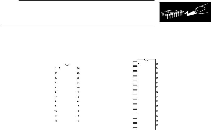
PIN CONFIGURATIONS
DIP and SOIC/TSSOP |
SSOP |
||
|
|
|
|
|
|
|
|
SCLK |
|
|
|
|
|
DGND |
|
|
|
|
|
||
MCLK IN |
|
|
|
|
|
DVDD |
|
|
|
|
|
||
|
|
|
|
|
||
MCLK OUT |
|
|
|
|
|
DIN |
|
|
|
|
|
||
POL |
|
|
|
|
|
DOUT |
|
|
|
|
|
||
|
|
|
|
|
||
SYNC |
|
AD7714 |
|
DRDY |
||
|
|
|||||
|
|
|||||
RESET |
|
|
CS |
|||
|
|
|||||
|
TOP VIEW |
|
||||
AIN1 |
|
|
AGND |
|||
|
(Not to Scale) |
|
||||
AIN2 |
|
|
|
|
|
AIN6 |
|
|
|
|
|
||
AIN3 |
|
|
|
|
|
AIN5 |
|
|
|
|
|
||
|
|
|
|
|
||
AIN4 |
|
|
|
|
|
REF IN(+) |
|
|
|
|
|
||
|
|
|
|
|
||
STANDBY |
|
|
|
|
|
REF IN(–) |
|
|
|
|
|
||
AVDD |
|
|
|
|
|
BUFFER |
|
|
|
|
|
||
|
|
|
|
|
|
|
SCLK 
 MCLK IN
 MCLK OUT
 POL
POL 

SYNC 

RESET 

NC 

NC 
 AIN1
AIN1 
 AIN2
AIN2 
 AIN3
AIN3 
 AIN4
AIN4 

STANDBY 

AVDD 

|
|
DGND |
|
|
DVDD |
|
|
|
|
|
DIN |
|
|
|
|
|
DOUT |
|
|
|
|
|
DRDY |
|
|
|
|
|
|
AD7714 |
|
CS |
|
||
|
NC |
|
|
||
TOP VIEW |
|
|
|
NC |
|
|
||
(Not to Scale) |
|
|
|
|
AGND |
|
|
|
|
|
AIN6 |
|
|
|
|
|
|
|
|
AIN5 |
|
|
|
|
|
|
|
|
REF IN(+) |
|
|
|
|
|
|
|
|
REF IN(–) |
|
|
|
|
|
|
|
|
BUFFER |
|
|
|
|
|
|
|
|
|
NC = NO CONNECT
–8– |
REV. C |

AD7714
|
|
PIN FUNCTION DESCRIPTION |
|
DIP/SOIC PIN NUMBERS |
|||
|
|
|
|
Pin |
|
|
|
No. |
Mnemonic |
Function |
|
|
|
|
|
1 |
SCLK |
Serial Clock. Logic Input. An external serial clock is applied to this input to access serial data from the |
|
|
|
AD7714. This serial clock can be a continuous clock with all data transmitted in a continuous train of pulses. |
|
|
|
Alternatively, it can be a noncontinuous clock with the information being transmitted to the AD7714 in smaller |
|
|
|
batches of data. |
|
2 |
MCLK IN |
Master Clock signal for the device. This can be provided in the form of a crystal/resonator or external clock. A |
|
|
|
crystal/resonator can be tied across the MCLK IN and MCLK OUT pins. Alternatively, the MCLK IN pin can |
|
|
|
be driven with a CMOS-compatible clock and MCLK OUT left unconnected. The part is specified with clock |
|
|
|
input frequencies of both 1 MHz and 2.4576 MHz. |
|
3 |
MCLK OUT |
When the master clock for the device is a crystal/resonator, the crystal/resonator is connected between MCLK |
|
|
|
IN and MCLK OUT. If an external clock is applied to the MCLK IN, MCLK OUT provides an inverted clock |
|
|
|
signal. This clock can be used to provide a clock source for external circuits. |
|
4 |
POL |
Clock Polarity. Logic Input. With this input low, the first transition of the serial clock in a data transfer |
|
|
|
operation is from a low to a high. In microcontroller applications, this means that the serial clock should idle |
|
|
|
low between data transfers. With this input high, the first transition of the serial clock in a data transfer |
|
|
|
operation is from a high to a low. In microcontroller applications, this means that the serial clock should idle |
|
|
|
high between data transfers. |
|
5 |
SYNC |
Logic Input which allows for synchronization of the digital filters and analog modulators when using a number |
|
|
|
of AD7714s. While SYNC is low, the nodes of the digital filter, the filter control logic and the calibration |
|
|
|
control logic are reset and the analog modulator is also held in its reset state. SYNC does not affect the digital |
|
|
|
interface and does not reset DRDY if it is low. |
|
6 |
RESET |
Logic Input. Active low input which resets the control logic, interface logic, digital filter and analog modulator |
|
|
|
of the part to power-on status. |
|
7 |
AIN1 |
Analog Input Channel 1. Programmable-gain analog input which can be used as a pseudo-differential input |
|
|
|
when used with AIN6 or as the positive input of a differential analog input pair when used with AIN2 (see |
|
|
|
Communications Register section). |
|
8 |
AIN2 |
Analog Input Channel 2. Programmable-gain analog input which can be used as a pseudo-differential input |
|
|
|
when used with AIN6 or as the negative input of a differential analog input pair when used with AIN1 (see |
|
|
|
Communications Register section). |
|
9 |
AIN3 |
Analog Input Channel 3. Programmable-gain analog input which can be used as a pseudo-differential input |
|
|
|
when used with AIN6 or as the positive input of a differential analog input pair when used with AIN4 (see |
|
|
|
Communications Register section). |
|
10 |
AIN4 |
Analog Input Channel 4. Programmable-gain analog input which can be used as a pseudo-differential input |
|
|
|
when used with AIN6 or as the negative input of a differential analog input pair when used with AIN3 (see |
|
|
|
Communications Register section). |
|
11 |
STANDBY |
Logic Input. Taking this pin low shuts down the analog and digital circuitry, reducing current consumption to |
|
|
|
typically 5 A. |
|
12 |
AVDD |
Analog Positive Supply Voltage, A Grade Versions: +3.3 V nominal (AD7714-3) or +5 V nominal (AD7714-5); |
|
|
|
Y Grade Versions: 3 V or 5 V nominal. |
|
13 |
BUFFER |
Buffer Option Select. Logic Input. With this input low, the on-chip buffer on the analog input (after the |
|
|
|
multiplexer and before the analog modulator) is shorted out. With the buffer shorted out the current flowing in |
|
|
|
the AVDD line is reduced to 270 A. With this input high, the on-chip buffer is in series with the analog input |
|
|
|
allowing the inputs to handle higher source impedances. |
|
14 |
REF IN(–) |
Reference Input. Negative input of the differential reference input to the AD7714. The REF IN(–) can lie |
|
|
|
anywhere between AVDD and AGND provided REF IN(+) is greater than REF IN(–). |
|
15 |
REF IN(+) |
Reference Input. Positive input of the differential reference input to the AD7714. The reference input is |
|
|
|
differential with the provision that REF IN(+) must be greater than REF IN(–). REF IN(+) can lie anywhere |
|
|
|
between AVDD and AGND. |
|
16 |
AIN5 |
Analog Input Channel 5. Programmable-gain analog input which is the positive input of a differential analog |
|
|
|
input pair when used with AIN6 (see Communications Register section). |
|
17 |
AIN6 |
Analog Input Channel 6. Reference point for AIN1 through AIN4 in pseudo-differential mode or as the |
|
|
|
negative input of a differential input pair when used with AIN5 (see Communications Register section). |
|
18 |
AGND |
Ground reference point for analog circuitry. |
|
|
|
|
|
REV. C |
–9– |
AD7714
|
|
PIN FUNCTION DESCRIPTION (Continued) |
Pin |
|
|
No. |
Mnemonic |
Function |
|
|
|
19 |
CS |
Chip Select. Active low Logic Input used to select the AD7714. With this input hard-wired low, the AD7714 |
|
|
can operate in its three-wire interface mode with SCLK, DIN and DOUT used to interface to the device. CS |
|
|
can be used to select the device in systems with more than one device on the serial bus or as a frame |
|
|
synchronization signal in communicating with the AD7714. |
20 |
DRDY |
Logic output. A logic low on this output indicates that a new output word is available from the AD7714 data |
|
|
register. The DRDY pin will return high upon completion of a read operation of a full output word. If no data |
|
|
read has taken place, after an output update, the DRDY line will return high for 500 × tCLK INcycles prior to |
|
|
the next output update. This gives an indication of when a read operation should not be attempted to avoid |
|
|
reading from the data register as it is being updated. DRDY is also used to indicate when the AD7714 has |
|
|
completed its on-chip calibration sequence. |
21 |
DOUT |
Serial Data Output with serial data being read from the output shift register on the part. This output shift |
|
|
register can contain information from the calibration registers, mode register, communications register, filter |
|
|
selection registers or data register depending on the register selection bits of the Communications Register. |
22 |
DIN |
Serial Data Input with serial data being written to the input shift register on the part. Data from this input shift |
|
|
register is transferred to the calibration registers, mode register, communications register or filter selection |
|
|
registers depending on the register selection bits of the Communications Register. |
23 |
DVDD |
Digital Supply Voltage, A Grade Versions: +3.3 V or +5 V nominal; Y Grade Versions: 3 V or 5 V nominal. |
24 |
DGND |
Ground reference point for digital circuitry. |
|
|
|
TERMINOLOGY*
INTEGRAL NONLINEARITY
This is the maximum deviation of any code from a straight line passing through the endpoints of the transfer function. The endpoints of the transfer function are zero scale (not to be confused with bipolar zero), a point 0.5 LSB below the first code transition (000 . . . 000 to 000 . . . 001) and full scale, a point
0.5 LSB above the last code transition (111 . . . 110 to
111 . . . 111). The error is expressed as a percentage of full scale.
POSITIVE FULL-SCALE ERROR
Positive Full-Scale Error is the deviation of the last code transition (111 . . . 110 to 111 . . . 111) from the ideal AIN(+) voltage (AIN(–) + VREF/GAIN – 3/2 LSBs). It applies to both unipolar and bipolar analog input ranges.
UNIPOLAR OFFSET ERROR
Unipolar Offset Error is the deviation of the first code transition from the ideal AIN(+) voltage (AIN(–) + 0.5 LSB) when operating in the unipolar mode.
BIPOLAR ZERO ERROR
This is the deviation of the midscale transition (0111 . . . 111 to 1000 . . . 000) from the ideal AIN(+) voltage (AIN(–) – 0.5 LSB) when operating in the bipolar mode.
GAIN ERROR
This is a measure of the span error of the ADC. It includes fullscale errors but not zero-scale errors. For unipolar input ranges it is defined as (full-scale error – unipolar offset error) while for bipolar input ranges it is defined as (full-scale error – bipolar zero error).
*AIN(–) refers to the negative input of the differential input pairs or to AIN6 when referring to the pseudo-differential input configurations.
BIPOLAR NEGATIVE FULL-SCALE ERROR
This is the deviation of the first code transition from the ideal AIN(+) voltage (AIN(–) – VREF/GAIN + 0.5 LSB) when operating in the bipolar mode.
POSITIVE FULL-SCALE OVERRANGE
Positive Full-Scale Overrange is the amount of overhead available to handle input voltages on AIN(+) input greater than AIN(–) + VREF/GAIN (for example, noise peaks or excess voltages due to system gain errors in system calibration routines) without introducing errors due to overloading the analog modulator or overflowing the digital filter.
NEGATIVE FULL-SCALE OVERRANGE
This is the amount of overhead available to handle voltages on AIN(+) below AIN(–) – VREF/GAIN without overloading the analog modulator or overflowing the digital filter. Note that the analog input will accept negative voltage peaks even in the unipolar mode provided that AIN(+) is greater than AIN(–) and greater than AGND – 30 mV.
OFFSET CALIBRATION RANGE
In the system calibration modes, the AD7714 calibrates its offset with respect to the analog input. The Offset Calibration Range specification defines the range of voltages that the AD7714 can accept and still calibrate offset accurately.
FULL-SCALE CALIBRATION RANGE
This is the range of voltages that the AD7714 can accept in the system calibration mode and still calibrate full scale correctly.
INPUT SPAN
In system calibration schemes, two voltages applied in sequence to the AD7714’s analog input define the analog input range. The input span specification defines the minimum and maximum input voltages from zero to full scale that the AD7714 can accept and still calibrate gain accurately.
–10– |
REV. C |

AD7714
AD7714-5 OUTPUT NOISE
Table Ia shows the output rms noise and effective resolution for some typical notch and –3 dB frequencies for the AD7714-5 with
f = 2.4576 MHz while Table Ib gives the information for f = 1 MHz. The numbers given are for the bipolar input ranges
CLK IN CLK IN
with a VREF of +2.5 V and with BUFFER = 0. These numbers are typical and are generated at an analog input voltage of 0 V. The numbers in brackets in each table are for the effective resolution of the part (rounded to the nearest 0.5 LSB). The effectiveresolution of the device is defined as the ratio of the output rms noise to the input full scale (i.e., 2 × VREF/GAIN). It should be noted that it is not calculated using peak-to-peak output noise numbers. Peak-to-peak noise numbers can be up to 6.6 times the rms numbers while effective resolution numbers based on peak-to-peak noise can be 2.5 bits below the effective resolution based on rms noise as quoted in the tables.
The output noise from the part comes from two sources. The first is the electrical noise in the semiconductor devices used in the implementation of the modulator (device noise). Secondly, when the analog input signal is converted into the digital domain, quantization noise is added. The device noise is at a low level and is largely independent of frequency. The quantization noise starts at an even lower level but rises rapidly with increasing frequency to become the dominant noise source. Consequently, lower filter
notch settings (below 100 Hz approximately for f = 2.4576 MHz and below 40 Hz approximately for f = 1 MHz) tend to
CLK IN CLK IN
be device noise dominated while higher notch settings are dominated by quantization noise. Changing the filter notch and cutoff frequency in the quantization-noise dominated region results in a more dramatic improvement in noise performance than it does in the device-noise dominated region as shown in Table I. Furthermore, quantization noise is added after the PGA, so effective resolution is largely independent of gain for the higher filter notch frequencies. Meanwhile, device noise is added in the PGA and, therefore, effective resolution reduces at high gains for lower notch frequencies. Additionally, in the device-noise dominated region, the output noise (in µV) is largely independent of reference voltage while in the quantization-noise dominated region, the noise is proportional to the value of the reference. It is possible to do post-filtering on the device to improve the output data rate for a given
–3 dB frequency and also to further reduce the output noise.
At the lower filter notch settings (below 60 |
Hz forCLKf IN = 2.4576 MHz and below 25 |
Hz forCLKf IN = 1 MHz), the no missing |
||||||||||||||||||||||||||
codes performance of the device is at the 24-bit level. At the higher settings, more codes will be missed until at 1 |
kHz notchsetting |
|||||||||||||||||||||||||||
for fCLK IN= 2.4576 |
MHz (400 Hz forCLKf |
IN = 1 MHz), no missing codes performance is only guaranteed to the 12-bit level. |
|
|
|
|||||||||||||||||||||||
|
|
Table Ia. AD7714-5 Output Noise/Resolution vs. Gain and First Notch for fCLK IN = 2.4576 |
MHz, BUFFER = 0 |
|
|
|
||||||||||||||||||||||
|
|
|
|
|
|
|
|
|
|
|
|
|
|
|
|
|
|
|
|
|
|
|
|
|
|
|
|
|
Filter First |
|
|
|
|
|
|
|
|
Typical Output RMS Noise in mV (Effective Resolution in Bits) |
|
|
|
|
|
|
|||||||||||||
|
|
|
|
|
|
|
|
|
|
|
|
|
|
|
|
|
|
|
|
|
|
|
|
|
|
|||
Notch & O/P |
|
–3 dB |
|
Gain of |
|
Gain of |
Gain of |
Gain of |
Gain of |
|
Gain of |
Gain of |
Gain of |
|||||||||||||||
Data Rate |
|
Frequency |
1 |
|
|
2 |
|
4 |
|
8 |
|
16 |
|
|
32 |
|
64 |
|
|
128 |
|
|
|
|||||
|
|
|
|
|
|
|
|
|
|
|
|
|
|
|
|
|
|
|
|
|
|
|
|
|
|
|
|
|
5 |
Hz |
|
1.31 |
|
Hz |
0.87 |
(22.5) |
|
0.48 |
|
(22.5) |
0.24 |
(22.5) |
0.2 |
(21.5) |
0.18 |
(20.5) |
0.17 |
(20) |
0.17 |
(19) |
0.17 |
(18) |
|
|
|||
10 |
|
Hz |
|
2.62 |
|
Hz |
1.0 |
(22.5) |
|
0.78 |
|
(21.5) |
0.48 |
(21.5) |
0.33 |
(21) |
0.25 |
(20.5) |
0.25 |
(19.5) |
0.25 |
(18.5) |
0.25 |
(17.5) |
||||
25 |
|
Hz |
|
6.55 |
|
Hz |
1.8 |
(21.5) |
|
1.1 |
|
(21) |
0.63 |
(21) |
0.5 |
(20) |
0.44 |
(19.5) |
0.41 |
(18.5) |
0.38 (17.5) 0.38 |
(16.5) |
||||||
30 |
|
Hz |
|
7.86 |
|
Hz |
2.5 |
(21) |
|
1.31 |
|
(21) |
0.84 |
(20.5) |
0.57 |
(20) |
0.46 |
(19.5) |
0.43 |
(18.5) |
0.4 |
|
(17.5) 0.4 |
(16.5) |
||||
50 |
|
Hz |
|
13.1 |
|
Hz |
4.33 |
(20) |
|
2.06 |
|
(20) |
1.2 |
(20) |
0.64 |
(20) |
0.54 |
(19) |
|
0.46 |
(18.5) |
0.46 |
(17.5) |
0.46 |
(16.5) |
|||
60 |
|
Hz |
|
15.72 |
Hz |
5.28 |
(20) |
|
2.36 |
|
(20) |
1.33 (20) |
0.87 |
(19.5) |
0.63 |
(19) |
|
0.62 |
(18) |
0.6 |
|
(17) |
0.56 |
(16) |
|
|
||
100 |
Hz |
|
26.2 |
|
Hz |
12.1 |
(18.5) |
|
5.9 |
|
(18.5) |
2.86 |
(19) |
1.91 |
(18.5) |
1.06 |
(18) |
|
0.83 |
(17.5) |
0.82 |
(16.5) |
0.76 |
(15.5) |
||||
250 |
Hz |
|
65.5 |
|
Hz |
127 |
(15.5) |
|
58 |
|
(15.5) |
29 |
(15.5) |
15.9 |
(15.5) |
6.7 |
(15.5) |
3.72 |
(15.5) |
1.96 |
(15.5) 1.5 |
(14.5) |
||||||
500 |
Hz |
|
131 |
Hz |
533 |
(13) |
|
267 |
|
(13) |
137 |
(13) |
66 |
(13) |
38 |
(13) |
|
20 |
(13) |
8.6 |
|
(13) |
4.4 |
(13) |
|
|
||
1 |
kHz |
|
262 |
Hz |
2,850 (11) |
|
1,258 (11) |
680 |
(11) |
297 |
(11) |
131 |
(11) |
|
99 |
(10.5) |
53 |
|
(10.5) |
28 |
(10.5) |
|||||||
|
|
|
|
|
|
|
|
|
|
|
|
|
|
|
|
|
|
|
|
|
|
|
|
|||||
|
|
|
Table Ib. AD7714-5 Output Noise/Resolution vs. Gain and First Notch for fCLK IN = 1 MHz, BUFFER = 0 |
|
|
|
|
|||||||||||||||||||||
|
|
|
|
|
|
|
|
|
|
|
|
|
|
|
|
|
|
|
|
|
|
|
|
|
|
|
|
|
Filter First |
|
|
|
|
|
|
|
|
Typical Output RMS Noise in mV (Effective Resolution in Bits) |
|
|
|
|
|
|
|||||||||||||
Notch & O/P |
|
–3 dB |
|
Gain of |
|
Gain of |
Gain of |
Gain of |
Gain of |
|
Gain of |
Gain of |
Gain of |
|||||||||||||||
Data Rate |
|
Frequency |
1 |
|
|
2 |
|
4 |
|
8 |
|
16 |
|
|
32 |
|
64 |
|
|
128 |
|
|
|
|||||
|
|
|
|
|
|
|
|
|
|
|
|
|
|
|
|
|
|
|
|
|
|
|
|
|
|
|
|
|
2 |
Hz |
|
0.52 |
|
Hz |
0.75 |
(22.5) |
|
0.56 |
|
(22) |
0.31 |
(22) |
0.19 |
(21.5) |
0.17 |
(21) |
|
0.14 |
(20) |
0.14 |
(19) |
0.14 |
(18) |
|
|
||
4 |
Hz |
|
1.05 |
|
Hz |
1.04 |
(22) |
|
0.88 |
|
(21.5) |
0.45 |
(21.5) |
0.28 |
(21) |
0.21 |
(20.5) |
|
0.21 |
(19.5) |
0.21 |
(18.5) |
0.21 |
(17.5) |
||||
10 |
|
Hz |
|
2.62 |
|
Hz |
1.66 |
(21.5) |
|
1.01 |
|
(21.5) |
0.77 |
(20.5) |
0.41 |
(20.5) |
0.37 |
(19.5) |
|
0.35 |
(19) |
0.35 |
(18) |
0.35 |
(17) |
|
|
|
25 Hz |
|
6.55 |
Hz |
5.2 |
(20) |
|
2.06 |
|
(20) |
1.4 (20) |
0.86 |
(19.5) |
0.63 |
(19) |
|
0.61 |
(18) |
0.59 |
(17) 0.59 |
(16) |
|
|
||||||
30 |
|
Hz |
|
7.86 |
|
Hz |
7.1 |
(19.5) |
|
3.28 |
|
(19.5) |
1.42 |
(19.5) |
1.07 |
(19) |
0.78 |
(18.5) |
|
0.64 |
(18) |
0.61 (17) |
0.61 |
(16) |
|
|
||
50 |
|
Hz |
|
13.1 |
|
Hz |
19.4 |
(18) |
|
9.11 |
|
(18) |
4.2 |
(18) |
2.45 |
(18) |
1.56 |
(17.5) |
|
1.1 |
(17) |
0.82 |
(16.5) |
0.8 |
(15.5) |
|||
60 |
|
Hz |
|
15.72 |
Hz |
25 |
(17.5) |
|
16 |
|
(17.5) |
6.5 |
(17.5) |
2.9 |
(17.5) |
1.93 |
(17.5) |
|
1.4 |
(17) |
1.1 |
|
(16) |
0.98 |
(15.5) |
|||
100 |
Hz |
|
26.2 |
|
Hz |
102 |
(15.5) |
|
58 |
|
(15.5) |
25 |
(15.5) |
13.5 |
(15.5) |
5.7 |
(15.5) |
|
3.9 |
(15.5) |
2.1 |
|
(15) |
1.3 |
(15) |
|
|
|
200 |
Hz |
|
52.4 |
|
Hz |
637 |
(13) |
|
259 |
|
(13) |
130 |
(13) |
76 |
(13) |
33 |
(13) |
|
16 |
(13) |
11 |
|
(13) |
6 |
(12.5) |
|||
400 |
Hz |
|
104.8 |
Hz |
2,830 |
(11) |
|
1,430 (11) |
720 |
(11) |
334 |
(11) |
220 |
(10.5) |
|
94 |
(10.5) |
54 |
|
(10.5) |
25 |
(10.5) |
||||||
|
|
|
|
|
|
|
|
|
|
|
|
|
|
|
|
|
|
|
|
|
|
|
|
|
|
|
|
|
REV. C |
–11– |

AD7714
AD7714-3 OUTPUT NOISE
Table IIa shows the output rms noise and effective resolution for some typical notch and –3 dB frequencies for the AD7714-3 with
f = 2.4576 MHz while Table IIb gives the information for f = 1 MHz. The numbers given are for the bipolar input
CLK IN CLK IN
ranges with a VREF of +1.25 V and BUFFER = 0. These numbers are typical and are generated at an analog input voltage of 0 V. The numbers in brackets in each table are for the effective resolution of the part (rounded to the nearest 0.5 LSB). The effective resolution of the device is defined as the ratio of the output rms noise to the input full scale (i.e., 2 × VREF/GAIN). It should be noted that it is not calculated using peak-to-peak output noise numbers. Peak-to-peak noise numbers can be up to 6.6 times the rms numbers while effective resolution numbers based on peak-to-peak noise can be 2.5 bits below the effective resolution based on rms noise as quoted in the tables.
The output noise from the part comes from two sources. The first is the electrical noise in the semiconductor devices used in the implementation of the modulator (device noise). Secondly, when the analog input signal is converted into the digital domain, quantization noise is added. The device noise is at a low level and is largely independent of frequency. The quantization noise starts at an even lower level but rises rapidly with increasing frequency to become the dominant noise source. Consequently, lower filter
notch settings (below 100 Hz approximately for f = 2.4576 MHz and below 40 Hz approximately for f = 1 MHz) tend to
CLK IN CLK IN
be device noise dominated while higher notch settings are dominated by quantization noise. Changing the filter notch and cutoff frequency in the quantization noise dominated region results in a more dramatic improvement in noise performance than it does in the device-noise dominated region as shown in Table II. Furthermore, quantization noise is added after the PGA, so effective resolution is largely independent of gain for the higher filter notch frequencies. Meanwhile, device noise is added in the PGA and, therefore, effective resolution suffers a little at high gains for lower notch frequencies. Additionally, in the device-noise dominated region, the output noise (in µV) is largely independent of reference voltage while in the quantization-noise dominated region, the noise is
proportional to the value of the reference. |
It is possible to do post-filtering on the device to improve the output data rate for a given |
||||||||||||||||||||||||||
–3 dB frequency and also to further reduce the output noise. |
|
|
|
|
|
|
|
|
|
|
|
|
|
|
|||||||||||||
At the lower filter notch settings (below 60 |
Hz forCLKf IN = 2.4576 MHz and below 25 Hz forCLKf IN = 1 MHz), the no missing |
||||||||||||||||||||||||||
codes performance of the device is at the 24-bit level. At the higher settings, more codes will be missed until at 1 |
kHz notchsetting |
||||||||||||||||||||||||||
for fCLK IN= 2.4576 |
MHz (400 Hz forCLKf |
IN = 1 MHz), no missing codes performance is only guaranteed to the 12-bit level. |
|
|
|
||||||||||||||||||||||
|
|
|
Table IIa. AD7714-3 Output Noise/Resolution vs. Gain and First Notch for fCLK IN = 2.4576 |
MHz, BUFFER = 0 |
|
|
|
||||||||||||||||||||
|
|
|
|
|
|
|
|
|
|
|
|
|
|
|
|
|
|
|
|
|
|
|
|
||||
Filter First |
|
|
|
|
|
|
|
Typical Output RMS Noise in mV (Effective Resolution in Bits) |
|
|
|
|
|
|
|||||||||||||
Notch & O/P |
–3 dB |
Gain of |
|
Gain of |
Gain of |
Gain of |
Gain of |
Gain of |
Gain of |
Gain of |
|||||||||||||||||
Data Rate |
Frequency |
1 |
|
|
2 |
|
4 |
|
8 |
|
16 |
|
32 |
|
64 |
|
|
128 |
|
|
|
||||||
|
|
|
|
|
|
|
|
|
|
|
|
|
|
|
|
|
|
|
|
|
|
|
|
||||
5 |
Hz |
1.31 |
Hz |
1.07 |
|
(21) |
|
0.68 |
|
(21) |
0.29 |
(21) |
0.24 |
(20) |
0.22 |
(19.5) |
0.22 |
(18.5) |
0.22 |
(17.5) |
0.22 |
(16.5) |
|||||
10 |
|
Hz |
2.62 |
Hz |
1.69 |
|
(20.5) |
|
1.1 |
|
(20) |
0.56 |
(20) |
0.35 |
(19.5) |
0.33 |
(19) |
0.33 |
(18) |
0.33 |
(17) |
0.33 |
(16) |
|
|
||
25 |
|
Hz |
6.55 |
Hz |
3.03 |
|
(19.5) |
|
1.7 |
|
(19.5) |
0.89 |
(19.5) |
0.55 |
(19) |
0.49 |
(18.5) |
0.46 |
(17.5) |
0.46 |
(16.5) |
0.45 |
(15.5) |
||||
30 |
|
Hz |
7.86 |
Hz |
3.55 |
|
(19.5) |
|
2.1 |
|
(19) |
1.1 |
(19) |
0.61 |
(18.5) |
0.58 |
(18) |
0.57 |
(17) |
0.55 |
(16) |
0.55 |
(15) |
|
|
||
50 |
|
Hz |
13.1 |
Hz |
4.72 |
|
(19) |
|
2.3 |
|
(19) |
1.5 |
(18.5) |
0.84 |
(18.5) |
0.7 |
(18) |
0.68 |
(17) |
0.67 |
(16) |
0.66 |
(15) |
|
|
||
60 |
|
Hz |
15.72 Hz |
5.12 |
|
(19) |
|
3.1 |
|
(18.5) |
1.6 |
(18) |
0.98 |
(18) |
0.9 |
(17.5) |
0.7 |
(17) |
0.69 |
(16) |
0.68 |
(15) |
|
|
|||
100 |
Hz |
26.2 |
Hz |
9.68 |
|
(18) |
|
5.6 |
|
(18) |
2.4 |
(18) |
1.3 |
(18) |
1.1 |
(17) |
0.95 |
(16.5) |
0.88 |
(15.5) |
0.9 |
(14.5) |
|||||
250 |
Hz |
65.5 |
Hz |
44 |
|
(16) |
|
31 |
|
(15.5) |
15 |
(15.5) |
5.8 |
(15.5) |
3.7 |
(15.5) |
2.4 |
(15) |
1.8 |
|
(14.5) 1.8 |
(13.5) |
|||||
500 |
Hz |
131 |
Hz |
304 |
|
(13) |
|
129 |
|
(13) |
76 |
(13) |
33 |
(13) |
20 |
(13) |
11 |
(13) |
6.3 |
|
(12.5) |
3 |
(12.5) |
||||
1 |
kHz |
262 |
Hz |
1410 |
|
(11) |
|
715 |
|
(11) |
350 |
(11) |
177 |
(11) |
101 |
(10.5) |
51 |
(10.5) |
31 |
|
(10.5) |
12 |
(10.5) |
||||
|
|
|
|
|
|
|
|
|
|
|
|
|
|
|
|
|
|
|
|
|
|
|
|
|
|
|
|
|
|
|
Table IIb. AD7714-3 Output Noise/Resolution vs. Gain and First Notch for fCLK IN = 1 MHz, BUFFER = 0 |
|
|
|
|
||||||||||||||||||||
|
|
|
|
|
|
|
|
|
|
|
|
|
|
|
|
|
|
|
|
|
|
|
|
|
|
|
|
|
Filter First |
|
|
|
|
|
|
|
Typical Output RMS Noise in mV (Effective Resolution in Bits) |
|
|
|
|
|
|
||||||||||||
|
|
|
|
|
|
|
|
|
|
|
|
|
|
|
|
|
|
|
|
|
|
|
|
|
|||
|
Notch & O/P |
–3 dB |
Gain of |
|
Gain of |
Gain of |
Gain of |
Gain of |
Gain of |
Gain of |
Gain of |
||||||||||||||||
|
Data Rate |
Frequency |
1 |
|
|
2 |
|
4 |
|
8 |
|
16 |
|
32 |
|
64 |
|
|
128 |
|
|
|
|||||
|
|
|
|
|
|
|
|
|
|
|
|
|
|
|
|
|
|
|
|
|
|
|
|
|
|
|
|
2 |
Hz |
0.52 |
Hz |
0.86 |
|
(21.5) |
|
0.58 |
|
(21) |
0.32 |
(21) |
0.21 |
(20.5) |
0.2 |
(19.5) |
0.2 |
(18.5) |
0.2 |
|
(17.5) |
0.2 |
(16.5) |
||||
4 |
Hz |
1.05 |
Hz |
1.26 |
|
(21) |
|
0.74 |
|
(20.5) |
0.44 |
(20.5) |
0.35 |
(20) |
0.3 |
(19) |
0.3 |
(18) |
0.3 |
|
(17) |
0.3 |
(16) |
|
|
||
10 |
|
Hz |
2.62 |
Hz |
1.68 |
|
(20.5) |
|
1.33 |
|
(20) |
0.73 |
(20) |
0.5 |
(19) |
0.49 |
(18.5) |
0.49 |
(17.5) |
0.48 |
(16.5) |
0.47 |
(15.5) |
||||
25 |
|
Hz |
6.55 |
Hz |
3.82 |
|
(19.5) |
|
2.0 |
|
(19.5) |
1.2 |
(19) |
0.88 |
(18.5) |
0.66 |
(18) |
0.57 |
(17) |
0.55 |
(16) |
0.55 |
(15) |
|
|
||
30 |
|
Hz |
7.86 |
Hz |
4.88 |
|
(19) |
|
2.1 |
|
(19) |
1.3 |
(19) |
0.93 |
(18.5) |
0.82 |
(17.5) |
0.69 |
(17) |
0.68 |
(16) |
0.66 |
(15) |
|
|
||
50 |
|
Hz |
13.1 |
Hz |
11 |
|
(18) |
|
4.8 |
|
(18) |
2.4 |
(18) |
1.4 |
(18) |
1.4 |
(17) |
0.73 |
(16.5) |
0.71 |
(15.5) |
0.7 |
(15) |
|
|
||
60 |
|
Hz |
15.72 Hz |
14.7 |
|
(17.5) |
|
7.5 |
|
(17.5) |
3.8 |
(17.5) |
2.6 |
(17) |
1.5 |
(16.5) |
0.95 |
(16.5) |
0.88 |
(15) |
0.9 |
(14.5) |
|||||
100 |
Hz |
26.2 |
Hz |
61 |
|
(15.5) |
|
30 |
|
(15.5) |
12 |
(15.5) |
6.1 |
(15.5) |
2.9 |
(15.5) |
2.4 |
(15) |
1.8 |
|
(14.5) |
1.8 |
(13.5) |
||||
200 |
Hz |
52.4 |
Hz |
275 |
|
(13) |
|
130 |
|
(13) |
65 |
(13) |
33 |
(13) |
17 |
(13) |
11 |
(13) |
6.3 |
|
(12.5) 3 |
(12.5) |
|||||
|
400 Hz |
104.8 |
Hz |
1435 |
|
(11) |
|
720 |
|
(11) |
362 |
(11) |
175 |
(11) |
110 |
(10.5) |
51 |
(10.5) |
31 |
(10.5) 12 |
(10.5) |
|
|
||||
|
|
|
|
|
|
|
|
|
|
|
|
|
|
|
|
|
|
|
|
|
|
|
|
|
|
|
|
–12– |
REV. C |
Loading...