


 Loading...
Analog Devices AD7840SQ, AD7840KP, AD7840KN, AD7840JP, AD7840JN Datasheet
...a |
LC2MOS |
|
Complete 14-Bit DAC |
||
|
|
|
|
|
AD7840 |
|
|
|
FEATURES
Complete 14-Bit Voltage Output DAC Parallel and Serial Interface Capability 80 dB Signal-to-Noise Ratio
Interfaces to High Speed DSP Processors e.g., ADSP-2100, TMS32010, TMS32020
45 ns min WR Pulse Width Low Power – 70 mW typ. Operates from 65 V Supplies
GENERAL DESCRIPTION
The AD7840 is a fast, complete 14-bit voltage output D/A converter. It consists of a 14-bit DAC, 3 V buried Zener reference, DAC output amplifier and high speed control logic.
The part features double-buffered interface logic with a 14-bit input latch and 14-bit DAC latch. Data is loaded to the input latch in either of two modes, parallel or serial. This data is then transferred to the DAC latch under control of an asynchronous LDAC signal. A fast data setup time of 21 ns allows direct parallel interfacing to digital signal processors and high speed 16-bit microprocessors. In the serial mode, the maximum serial data clock rate can be as high as 6 MHz.
The analog output from the AD7840 provides a bipolar output range of ±3 V. The AD7840 is fully specified for dynamic performance parameters such as signal-to-noise ratio and harmonic distortion as well as for traditional dc specifications. Full power output signals up to 20 kHz can be created.
The AD7840 is fabricated in linear compatible CMOS (LC2MOS), an advanced, mixed technology process that combines precision bipolar circuits with low power CMOS logic. The part is available in a 24-pin plastic and hermetic dual-in-line package (DIP) and is also packaged in a 28-termi- nal plastic leaded chip carrier (PLCC).
REV. B
Information furnished by Analog Devices is believed to be accurate and reliable. However, no responsibility is assumed by Analog Devices for its use, nor for any infringements of patents or other rights of third parties which may result from its use. No license is granted by implication or otherwise under any patent or patent rights of Analog Devices.
FUNCTIONAL BLOCK DIAGRAM
PRODUCT HIGHLIGHTS
1. Complete 14-Bit D/A Function
The AD7840 provides the complete function for creating ac signals and dc voltages to 14-bit accuracy. The part features an on-chip reference, an output buffer amplifier and 14-bit D/A converter.
2. Dynamic Specifications for DSP Users
In addition to traditional dc specifications, the AD7840 is specified for ac parameters including signal-to-noise ratio and harmonic distortion. These parameters along with important timing parameters are tested on every device.
3. Fast, Versatile Microprocessor Interface
The AD7840 is capable of 14-bit parallel and serial interfacing. In the parallel mode, data setup times of 21 ns and write pulse widths of 45 ns make the AD7840 compatible with modern 16-bit microprocessors and digital signal processors. In the serial mode, the part features a high data transfer rate of 6 MHz.
One Technology Way, P.O. Box 9106, Norwood, MA 02062-9106, U.S.A. Tel: 617/329-4700 Fax: 617/326-8703
AD7840–SPECIFICATIONS |
(VDD = +5 V 6 5%, VSS = –5 V 6 5%, AGND = DGND = O V, REF IN = +3 V, RL = 2 kV, |
|||||||
CL = 100 pF. All specifications TMIN to TMAX unless othewise noted.) |
||||||||
Parameter |
J, A1 |
K, B1 |
|
S1 |
Units |
Test Conditions/Comments |
||
DYNAMIC PERFORMANCE2 |
|
|
|
|
|
|
||
Signal to Noise Ratio3 (SNR) |
76 |
78 |
|
76 |
dB min |
VOUT = 1 kHz Sine Wave, fSAMPLE = 100 kHz |
||
|
|
|
|
|
|
|
|
Typically 82 dB at +25°C for 0 < VOUT < 20 kHz4 |
Total Harmonic Distortion (THD) |
–78 |
–80 |
|
–78 |
dB max |
VOUT = 1 kHz Sine Wave, fSAMPLE = 100 kHz |
||
|
|
|
|
|
|
|
|
Typically –84 dB at +25°C for 0 < VOUT < 20 kHz4 |
Peak Harmonic or Spurious Noise |
–78 |
–80 |
|
–78 |
dB max |
VOUT = 1 kHz Sine Wave, fSAMPLE = 100 kHz |
||
|
|
|
|
|
|
|
|
Typically –84 dB at +25°C for 0 < VOUT < 20 kHz4 |
DC ACCURACY |
|
|
|
|
|
|
||
Resolution |
14 |
14 |
|
14 |
Bits |
|
||
Integral Nonlinearity |
±2 |
±1 |
|
±2 |
LSB max |
|
||
Differential Nonlinearity |
±0.9 |
±0.9 |
|
±0.9 |
LSB max |
Guaranteed Monotonic |
||
Bipolar Zero Error |
±10 |
±10 |
|
±10 |
LSB max |
|
||
Positive Full Scale Error5 |
±10 |
±10 |
|
±10 |
LSB max |
|
||
Negative Full Scale Error5 |
±10 |
±10 |
|
±10 |
LSB max |
|
||
REFERENCE OUTPUT6 |
|
|
|
|
|
|
||
REF OUT @ +25°C |
2.99 |
2.99 |
|
2.99 |
V min |
|
||
|
|
|
3.01 |
3.01 |
|
3.01 |
V max |
|
REF OUT TC |
±60 |
±60 |
|
±60 |
ppm/°C max |
|
||
Reference Load Change |
|
|
|
|
|
Reference Load Current Change (0–500 μA) |
||
( REF OUT vs. I) |
–1 |
–1 |
|
–1 |
mV max |
|||
|
|
|
|
|
|
|
|
|
REFERENCE INPUT |
|
|
|
|
|
3 V ± 5% |
||
Reference Input Range |
2.85 |
2.85 |
|
2.85 |
V min |
|||
|
|
|
3.15 |
3.15 |
|
3.15 |
V max |
|
Input Current |
50 |
50 |
|
50 |
μA max |
|
||
LOGIC INPUTS |
|
|
|
|
|
VDD = 5 V ± 5% |
||
Input High Voltage, VINH |
2.4 |
2.4 |
|
2.4 |
V min |
|||
Input Low Voltage, VINL |
0.8 |
0.8 |
|
0.8 |
V max |
VDD = 5 V ± 5% |
||
Input Current, IIN |
±10 |
±10 |
|
±10 |
μA max |
VIN = 0 V to VDD |
||
Input Current ( |
|
Input Only) |
±10 |
±10 |
|
±10 |
μA max |
VIN =VSS to VDD |
CS |
||||||||
Input Capacitance, CIN7 |
10 |
10 |
|
10 |
pF max |
|
||
ANALOG OUTPUT |
±3 |
±3 |
|
±3 |
|
|
||
Output Voltage Range |
|
V nom |
|
|||||
DC Output Impedance |
0.1 |
0.1 |
|
0.1 |
Ω typ |
|
||
Short-Circuit Current |
20 |
20 |
|
20 |
mA typ |
|
||
|
|
|
|
|
|
|
||
AC CHARACTERISTICS7 |
|
|
|
|
|
Settling Time to within ±1/2 LSB of Final Value |
||
Voltage Output Settling Time |
|
|
|
|
μs max |
|||
Positive Full-Scale Change |
4 |
4 |
|
4 |
Typically 2 μs |
|||
Negative Full-Scale Change |
4 |
4 |
|
4 |
μs max |
Typically 2.5 μs |
||
Digital-to-Analog Glitch Impulse |
10 |
10 |
|
10 |
nV secs typ |
|
||
Digital Feedthrough |
2 |
2 |
|
2 |
nV secs typ |
|
||
|
|
|
|
|
|
|
||
POWER REQUIREMENTS |
|
|
|
|
|
±5% for Specified Performance |
||
VDD |
+5 |
+5 |
|
+5 |
V nom |
|||
VSS |
–5 |
–5 |
|
–5 |
V nom |
±5% for Specified Performance |
||
IDD |
14 |
14 |
|
15 |
mA max |
Output Unloaded, SCLK = +5 V. Typically 10 mA |
||
ISS |
6 |
6 |
|
7 |
mA max |
Output Unloaded, SCLK = +5 V. Typically 4 mA |
||
Power Dissipation |
100 |
100 |
|
110 |
mW max |
Typically 70 mW |
||
|
|
|
|
|
|
|
|
|
NOTES
1Temperature ranges are as follows: J, K Versions, 0°C to +70°C; A, B Versions, –25°C to +85°C; S Version, –55°C to +125°C. 2VOUT (pk-pk) = ±3 V
3SNR calculation includes distortion and noise components. 4Using external sample-and-hold (see Testing the AD7840).
5Measured with respect to REF IN and includes bipolar offset error.
6For capacitive loads greater than 50 pF, a series resistor is required (see Internal Reference section). 7Sample tested @ +25°C to ensure compliance.
Specifications subject to change without notice.
–2– |
REV. B |

|
|
|
|
|
|
|
|
|
|
|
|
|
AD7840 |
|
|
|
|
|
|
|
|
|
|
|
|
|
|
|
|
TIMING CHARACTERISTICS1, 2 |
(VDD = +5 V 6 5%, VSS = –5 V 6 5%, AGND = DGND = 0 V.) |
|||||||||||||
|
Limit at TMIN, TMAX |
|
Limit at TMIN, TMAX |
|
|
|
|
|
|
|
|
|
|
|
Parameter |
(J, K, A, B Versions) |
|
(S Version) |
Units |
|
Conditions/Comments |
||||||||
|
|
|
|
|
|
|
|
|
|
|
|
|
|
|
t1 |
0 |
|
0 |
ns min |
|
|
to |
|
|
|
Setup Time |
|||
|
CS |
WR |
||||||||||||
t2 |
0 |
|
0 |
ns min |
|
CS to WR Hold Time |
||||||||
t3 |
45 |
|
50 |
ns min |
|
WR |
Pulse Width |
|||||||
t4 |
21 |
|
28 |
ns min |
|
Data Valid to |
WR |
Setup Time |
||||||
t5 |
10 |
|
15 |
ns min |
|
Data Valid to WR Hold Time |
||||||||
t6 |
40 |
|
40 |
ns min |
|
LDAC |
Pulse Width |
|||||||
t7 |
50 |
|
50 |
ns min |
|
SYNC |
to SCLK Falling Edge |
|||||||
t83 |
150 |
|
200 |
ns min |
SCLK Cycle Time |
|||||||||
t9 |
30 |
|
40 |
ns min |
|
Data Valid to SCLK Setup Time |
||||||||
t10 |
75 |
|
100 |
ns min |
|
Data Valid to SCLK Hold Time |
||||||||
t11 |
75 |
|
100 |
ns min |
|
SYNC to SCLK Hold Time |
||||||||
NOTES
1Timing specifications in bold print are 100% production tested. All other times are sample tested at +25°C to ensure compliance. All input signals are specified with tr = tf = 5 ns (10% to 90% of 5 V) and timed from a voltage level of 1.6 V.
2See Figures 6 and 8.
3SCLK mark/space ratio is 40/60 to 60/40.
Specifications subject to change without notice.
ABSOLUTE MAXIMUM RATINGS* |
|
|
VDD to AGND . . . . . . . . . . . . . . . . . . . |
. . . . |
. . –0.3 V to +7 V |
VSS to AGND . . . . . . . . . . . . . . . . . . . |
. . . . |
. . +0.3 V to –7 V |
AGND to DGND . . . . . . . . . . . . . . . . |
–0.3 V to VDD + 0.3 V |
|
VOUT to AGND . . . . . . . . . . . . . . . . . . . |
. . . . |
. . . . VSS to VDD |
REF OUT to AGND . . . . . . . . . . . . . . . |
. . . . |
. . . . 0 V to VDD |
REF IN to AGND . . . . . . . . . . . . . . . . |
–0.3 V to VDD + 0.3 V |
|
Digital Inputs to DGND . . . . . . . . . . . |
–0.3 V to VDD + 0.3 V |
|
Operating Temperature Range |
|
0°C to +70°C |
Commercial (J, K Versions) . . . . . . . . |
. . . . |
|
Industrial (A, B Versions) . . . . . . . . . . |
. . . . |
–25°C to +85°C |
Extended (S Version) . . . . . . . . . . . . . |
. . . |
–55°C to +125°C |
Storage Temperature Range . . . . . . . . . |
. . . |
–65°C to +150°C |
Lead Temperature (Soldering, 10 sec) . . |
. . . . |
. . . . . . +300°C |
Power Dissipation (Any Package) to +75°C . . |
. . . . . . 450 mW |
|
Derates above +75°C by . . . . . . . . . . . . |
. . . . |
. . . . 10 mW/°C |
*Stresses above those listed under “Absolute Maximum Ratings” may cause permanent damage to the device. This is a stress rating only and functional operation of the device at these or any other conditions above those listed in the operational sections of this specification is not implied. Exposure to absolute maximum rating conditions for extended periods may affect device reliability.
ORDERING GUIDE
|
|
|
Integral |
|
|
Temperature |
SNR |
Nonlinearity |
Package |
Model1 |
Range |
(dB) |
(LSB) |
Option2 |
|
|
|
|
|
AD7840JN |
0°C to +70°C |
78 min |
±2 max |
N-24 |
AD7840KN |
0°C to +70°C |
80 min |
±1 max |
N-24 |
AD7840JP |
0°C to +70°C |
78 min |
±2 max |
P-28A |
AD7840KP |
0°C to +70°C |
80 min |
±1 max |
P-28A |
AD7840AQ |
–25°C to +85°C |
78 min |
±2 max |
Q-24 |
AD7840ARS |
–25°C to +85°C |
78 min |
±2 max |
RS-24 |
AD7840BQ |
–25°C to +85°C |
80 min |
±1 max |
Q-24 |
AD7840SQ3 |
–55°C to +125°C |
78 min |
±2 max |
Q-24 |
NOTES
1To order MIL-STD-883, Class B processed parts, add /883B to part number. Contact your local sales office for military data sheet and availability.
2N = Plastic DIP; P = Plastic Leaded Chip Carrier; Q = Cerdip. 3This grade will be available to /883B processing only.
CAUTION
ESD (electrostatic discharge) sensitive device. Electrostatic charges as high as 4000 V readily accumulate on the human body and test equipment and can discharge without detection. Although the AD7840 features proprietary ESD protection circuitry, permanent damage may occur on devices subjected to high energy electrostatic discharges. Therefore, proper ESD precautions are recommended to avoid performance degradation or loss of functionality.
WARNING!
ESD SENSITIVE DEVICE
REV. B |
–3– |
AD7840
|
|
|
|
|
|
|
|
|
|
|
PIN FUNCTION DESCRIPTION |
|||||||
|
|
|
|
|
|
|
|
|
|
|
|
|
|
|
|
|
|
|
DIP |
|
|
|
|
|
|
|
|
|
|
|
|
|
|
|
|
|
|
Pin |
|
Pin |
|
|
|
|
|
|
|
|
|
|
|
|||||
No. |
|
Mnemonic |
|
Function |
||||||||||||||
|
|
|
|
|
|
|
|
|
|
|
|
|
|
|
|
|
|
|
1 |
|
|
/SERIAL |
Chip Select/Serial Input. When driven with normal logic levels, it is an active low logic input which is used |
||||||||||||||
|
CS |
|||||||||||||||||
|
|
|
|
|
|
|
|
|
in conjunction with |
WR |
to load parallel data to the input latch. For applications where |
CS |
is perma- |
|||||
|
|
|
|
|
|
|
|
|
nently low, an R, C is required for correct power-up (see LDAC input). If this input is tied to VSS, it de- |
|||||||||
|
|
|
|
|
|
|
|
|
fines the AD7840 for serial mode operation. |
|||||||||
2 |
|
|
|
|
|
|
|
Write/Frame Synchronization Input. In the parallel data mode, it is used in conjunction with |
|
to load |
||||||||
|
WR/SYNC |
CS |
||||||||||||||||
|
|
|
|
|
|
|
|
|
parallel data. In the serial mode of operation, this pin functions as a Frame Synchronization pulse with se- |
|||||||||
|
|
|
|
|
|
|
|
|
rial data expected after the falling edge of this signal. |
|||||||||
3 |
|
D13/SDATA |
Data Bit 13(MSB)/Serial Data. When parallel data is selected, this pin is the D13 input. In serial mode, |
|||||||||||||||
|
|
|
|
|
|
|
|
|
SDATA is the serial data input which is used in conjunction with SYNC and SCLK to transfer serial data |
|||||||||
|
|
|
|
|
|
|
|
|
to the AD7840 input latch. |
|||||||||
4 |
|
D12/SCLK |
Data Bit 12/Serial Clock. When parallel data is selected, this pin is the D12 input. In the serial mode, it is |
|||||||||||||||
|
|
|
|
|
|
|
|
|
the serial clock input. Serial data bits are latched on the falling edge of SCLK when SYNC is low. |
|||||||||
5 |
|
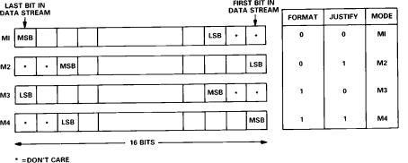
D11/FORMAT |
Data Bit 11/Data Format. When parallel data is selected, this pin is the D11 input. In serial mode, a Logic |
|||||||||||||||
|
|
|
|
|
|
|
|
|
1 on this input indicates that the MSB is the first valid bit in the serial data stream. A Logic 0 indicates |
|||||||||
|
|
|
|
|
|
|
|
|
that the LSB is the first valid bit (see Table I). |
|||||||||
6 |
|
D10/JUSTIFY |
Data Bit 10/Data Justification. When parallel data is selected, this pin is the D10 input. In serial mode, |
|||||||||||||||
|
|
|
|
|
|
|
|
|
this input controls the serial data justification (see Table I). |
|||||||||
7–11 |
D9–D5 |
Data Bit 9 to Data Bit 5. Parallel data inputs. |
||||||||||||||||
12 |
|
DGND |
Digital Ground. Ground reference for digital circuitry. |
|||||||||||||||
13–16 |
D4–D1 |
Data Bit 4 to Data Bit 1. Parallel data inputs. |
||||||||||||||||
17 |
|
D0 |
Data Bit 0 (LSB). Parallel data input. |
|||||||||||||||
18 |
|
VDD |
|
Positive Supply, +5 V ± 5%. |
||||||||||||||
19 |
|
AGND |
Analog Ground. Ground reference for DAC, reference and output buffer amplifier. |
|||||||||||||||
20 |
|
VOUT |
|
Analog Output Voltage. This is the buffer amplifier output voltage. Bipolar output range (±3 V with REF |
||||||||||||||
|
|
|
|
|
|
|
|
|
IN = +3 V). |
|||||||||
21 |
|
VSS |
|
Negative Supply Voltage, –5 V ± 5%. |
||||||||||||||
22 |
|
REF OUT |
|
Voltage Reference Output. The internal 3 V analog reference is provided at this pin. To operate the |
||||||||||||||
|
|
|
|
|
|
|
|
|
AD7840 with internal reference, REF OUT should be connected to REF IN. The external load capability |
|||||||||
|
|
|
|
|
|
|
|
|
of the reference is 500 μA. |
|||||||||
23 |
|
REF IN |
|
Voltage Reference Input. The reference voltage for the DAC is applied to this pin. It is internally buffered |
||||||||||||||
|
|
|
|
|
|
|
|
|
before being applied to the DAC. The nominal reference voltage for correct operation of the AD7840 is |
|||||||||
|
|
|
|
|
|
|
|
|
3 V. |
|||||||||
24 |
|
|
|
|
Load DAC. Logic Input. A new word is loaded into the DAC latch from the input latch on the falling |
|||||||||||||
|
LDAC |
|||||||||||||||||
|
|
|
|
|
|
|
|
|
edge of this signal (see Interface Logic Information section). The AD7840 should be powered-up with |
|||||||||
|
|
|
|
|
|
|
|
|
LDAC |
high. For applications where |
LDAC |
is permanently low, an R, C is required for correct power-up |
||||||
|
|
|
|
|
|
|
|
|
(see Figure 19). |
|||||||||
|
|
|
|
|
|
|
|
|
|
|
|
|
||||||
|
|
|
|
|
|
|
|
|
|
|
|
Table I. Serial Data Modes |
||||||
–4– |
REV. B |

AD7840
|
PIN CONFIGURATIONS |
DIP/SSOP |
PLCC |
D/A SECTION
The AD7840 contains a 14-bit voltage mode D/A converter consisting of highly stable thin film resistors and high speed NMOS single-pole, double-throw switches. The simplified circuit diagram for the DAC section is shown in Figure 1. The three MSBs of the data word are decoded to drive the seven switches A–G. The 11 LSBs switch an 11-bit R-2R ladder structure. The output voltage from this converter has the same polarity as the reference voltage, REF IN.
The REF IN voltage is internally buffered by a unity gain amplifier before being applied to the D/A converter and the bipolar bias circuitry. The D/A converter is configured and sealed for a 3 V reference and the device is tested with 3 V applied to REF IN. Operating the AD7840 at reference voltages outside the
±5% tolerance range may result in degraded performance from the part.
Figure 1. DAC Ladder Structure
INTERNAL REFERENCE
The AD7840 has an on-chip temperature compensated buried Zener reference (see Figure 2) which is factory trimmed to 3 V
±10 mV. The reference voltage is provided at the REF OUT pin. This reference can be used to provide both the reference voltage for the D/A converter and the bipolar bias circuitry. This is achieved by connecting the REF OUT pin to the REF IN pin of the device.
The reference voltage can also be used as a reference for other components and is capable of providing up to 500 μA to an external load. The maximum recommended capacitance on REF OUT for normal operation is 50 pF. If the reference is required
for external use, it should he decoupled to AGND with a 200 Ω resistor in series with a parallel combination of a 10 μF tantalum capacitor and a 0.1 μF ceramic capacitor.
Figure 2. Internal Reference
EXTERNAL REFERENCE
In some applications, the user may require a system reference or some other external reference to drive the AD7840 reference input. Figure 3 shows how the AD586 5 V reference can be conditioned to provide the 3 V reference required by the AD7840 REF IN. An alternate source of reference voltage for the AD7840 in systems which use both a DAC and an ADC is to use the REF OUT voltage of ADCs such as the AD7870 and AD7871. A circuit showing this arrangement is shown in Figure 20.
Figure 3. AD586 Driving AD7840 REF IN
REV. B |
–5– |
Loading...